BAT54 / 54A / 54C / 54S
Document Number 85508
Rev. 1.6, 24-Nov-04
Vishay Semiconductors
www.vishay.com
1
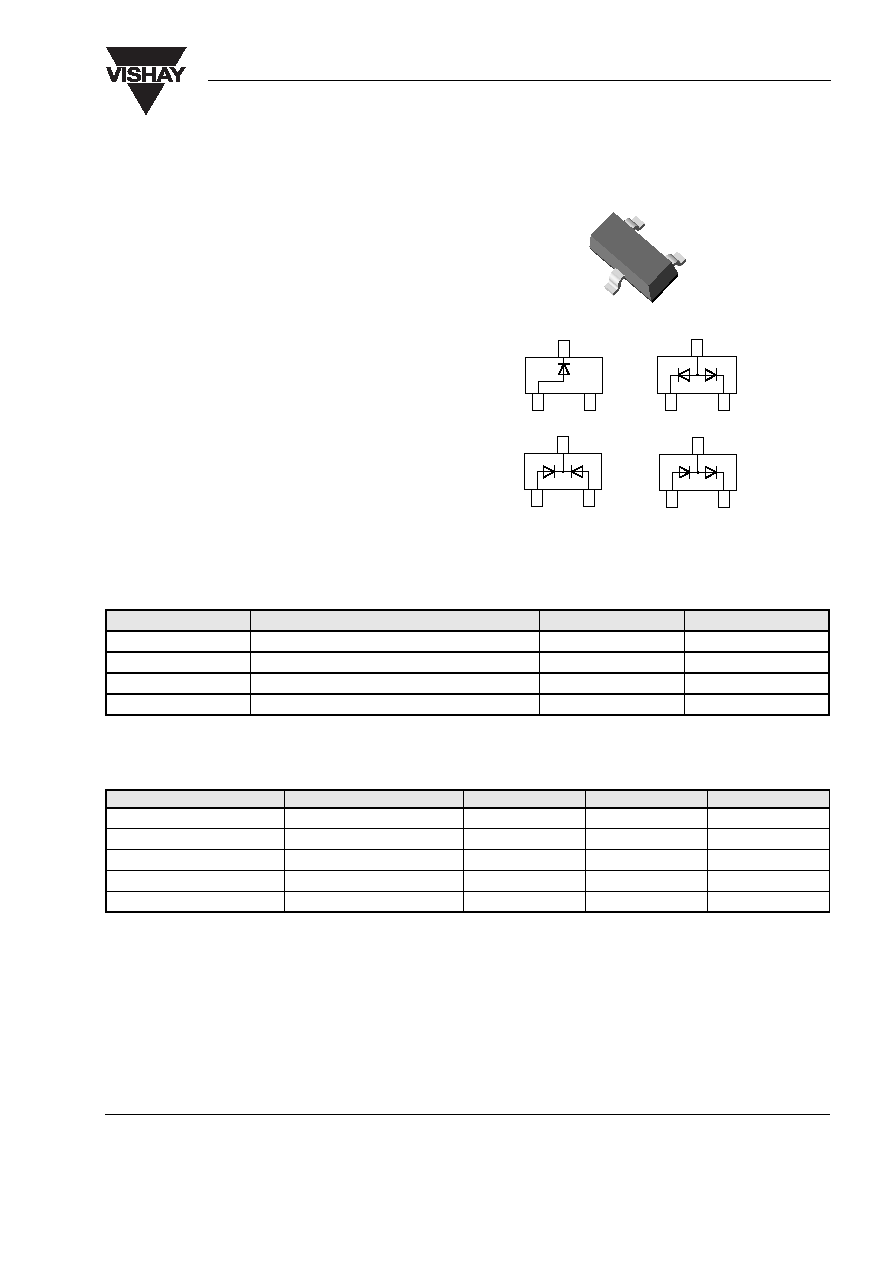
Top View
Top View
BAT54
BAT54C
BAT54A
BAT54S
18034
1
2
3
1
2
3
1
2
3
1
2
3
Small Signal Schottky Diodes, Single & Dual
Features
∑ These diodes feature very low turn-on voltage and
fast switching.
∑ These devices are protected by a PN junction
guard ring against excessive voltage, such as
electrostatic discharges.
Mechanical Data
Case: SOT-23 Plastic case
Weight: approx. 8.8 mg
Packaging Codes/Options:
GS18 / 10 k per 13" reel (8 mm tape), 10 k/box
GS08 / 3 k per 7" reel (8 mm tape), 15 k/box
Parts Table
Absolute Maximum Ratings
T
amb
= 25 ∞C, unless otherwise specified
1)
Device on fiberglass substrate, see layout on next page.
Part
Ordering code
Marking
Remarks
BAT54
BAT54-GS18 or BAT54-GS08
L4
Tape and Reel
BAT54A
BAT54A-GS18 or BAT54A-GS08
L42
Tape and Reel
BAT54C
BAT54C-GS18 or BAT54C-GS08
L43
Tape and Reel
BAT54S
BAT54S-GS18 or BAT54S-GS08
L44
Tape and Reel
Parameter
Test condition
Symbol
Value
Unit
Repetitive peak reverse voltage
V
RRM
30
V
Forward continuous current
I
F
200
1)
mA
Repetitive peak forward current
I
FRM
300
1)
mA
Surge forward current current
t
p
< 1 s
I
FSM
600
1)
mA
Power dissipation
P
tot
230
mW
www.vishay.com
2
Document Number 85508
Rev. 1.6, 24-Nov-04
BAT54 / 54A / 54C / 54S
Vishay Semiconductors
Thermal Characteristics
T
amb
= 25 ∞C, unless otherwise specified
1)
Device on fiberglass substrate, see layout on next page.
Electrical Characteristics
T
amb
= 25 ∞C, unless otherwise specified
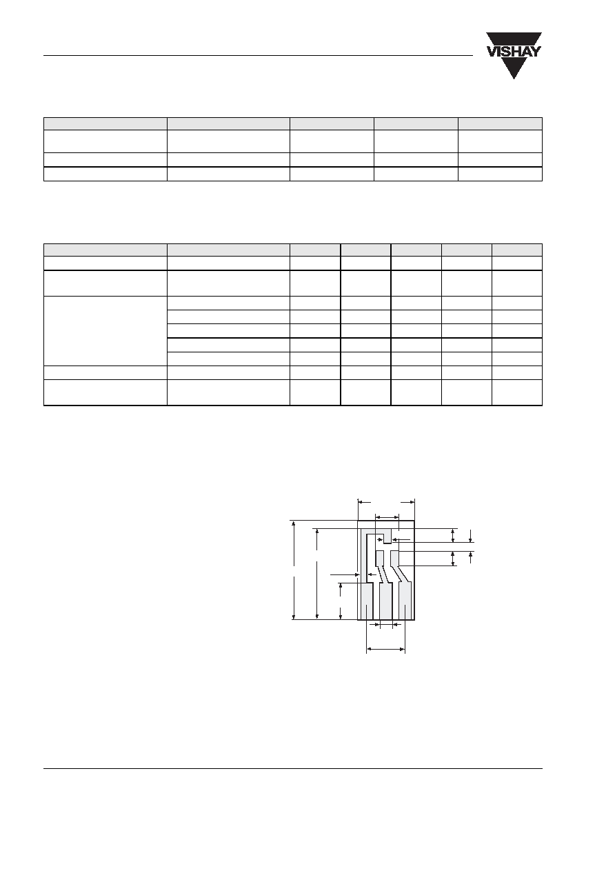
Layout for R
thJA
test
Thickness:
Fiberglass 1.5 mm (0.059 in.)
Copper leads 0.3 mm (0.012 in.)
Parameter
Test condition
Symbol
Value
Unit
Thermal resistance junction to
ambiant air
R
thJA
430
1)
∞C/W
Junction temperature
T
j
= T
stg
- 65 to + 150
∞C
Storage temperature range
T
S
- 65 to + 150
∞C
Parameter
Test condition
Symbol
Min
Typ.
Max
Unit
Reverse Breakdown voltage
I
R
= 100
µA pulses
V
(BR)
30
V
Leakage current
Pulse test t
p
< 300
µs, < 2 % at
V
R
= 25 V
I
R
2
µA
Forward voltage
I
F
= 0.1 mA, t
p
< 300
µs, < 2 %
V
F
240
mV
I
F
= 1 mA, t
p
< 300
µs, < 2 %
V
F
320
mV
I
F
= 10 mA, t
p
< 300
µs, < 2 %
V
F
400
mV
I
F
= 30 mA, t
p
< 300
µs, < 2 %
V
F
500
mV
I
F
= 100 mA, t
p
< 300
µs, < 2 %
V
F
1000
mV
Diode capacitance
V
R
= 1 V, f = 1 MHz
C
tot
10
pF
Reverse recovery time
I
F
= 10 mA through I
R
= 10 mA
to I
rr
= 1mA, R
L
= 100
t
rr
5
ns
17451
15 (0.59)
12 (0.47)
0.8 (0.03)
5 (0.2)
7.5 (0.3)
3 (0.12)
1 (0.4)
1 (0.4)
2 (0.8)
2 (0.8)
1.5 (0.06)
5.1 (0.2)

BAT54 / 54A / 54C / 54S
Document Number 85508
Rev. 1.6, 24-Nov-04
Vishay Semiconductors
www.vishay.com
5
Ozone Depleting Substances Policy Statement
It is the policy of Vishay Semiconductor GmbH to
1. Meet all present and future national and international statutory requirements.
2. Regularly and continuously improve the performance of our products, processes, distribution and
operatingsystems with respect to their impact on the health and safety of our employees and the public, as
well as their impact on the environment.
It is particular concern to control or eliminate releases of those substances into the atmosphere which are
known as ozone depleting substances (ODSs).
The Montreal Protocol (1987) and its London Amendments (1990) intend to severely restrict the use of ODSs
and forbid their use within the next ten years. Various national and international initiatives are pressing for an
earlier ban on these substances.
Vishay Semiconductor GmbH has been able to use its policy of continuous improvements to eliminate the use
of ODSs listed in the following documents.
1. Annex A, B and list of transitional substances of the Montreal Protocol and the London Amendments
respectively
2. Class I and II ozone depleting substances in the Clean Air Act Amendments of 1990 by the Environmental
Protection Agency (EPA) in the USA
3. Council Decision 88/540/EEC and 91/690/EEC Annex A, B and C (transitional substances) respectively.
Vishay Semiconductor GmbH can certify that our semiconductors are not manufactured with ozone depleting
substances and do not contain such substances.
We reserve the right to make changes to improve technical design
and may do so without further notice.
Parameters can vary in different applications. All operating parameters must be validated for each
customer application by the customer. Should the buyer use Vishay Semiconductors products for any
unintended or unauthorized application, the buyer shall indemnify Vishay Semiconductors against all
claims, costs, damages, and expenses, arising out of, directly or indirectly, any claim of personal
damage, injury or death associated with such unintended or unauthorized use.
Vishay Semiconductor GmbH, P.O.B. 3535, D-74025 Heilbronn, Germany
Telephone: 49 (0)7131 67 2831, Fax number: 49 (0)7131 67 2423

