 | ÐлекÑÑоннÑй компоненÑ: DG2015 | СкаÑаÑÑ:  PDF PDF  ZIP ZIP |
Äîêóìåíòàöèÿ è îïèñàíèÿ www.docs.chipfind.ru
INA
NO4
NC2
NO2
NO3
INB
NO1
NC4
1
2
3
12
11
10
4
9
5
6
7
8
16
15
14
13
COM2 V+ COM3 NC3
NC1 COM1 GND COM4
Top View
DG2015
QFN-16 (4 X 4)
DG2015
Vishay Siliconix
New Product
Document Number: 71971
S-03423--Rev. B, 03-Mar-03
www.vishay.com
1
Low-Voltage, Low r
ON
, Dual DPDT Analog Switch
FEATURES
D
Low Voltage Operation (2.7 V to 3.3 V)
D
Low On-Resistance - r
ON:
0.85
W
D
3 dB Loss @ 100 MHz
D
Fast Switching:
t
ON
= 40 ns
t
OFF
= 35 ns
D
QFN-16 Package
BENEFITS
D
Reduced Power Consumption
D
High Accuracy
D
Reduce Board Space
D
TTL/1.8-V Logic Compatible
D
High Bandwidth
APPLICATIONS
D
Cellular Phones
D
Speaker Headset Switching
D
Audio and Video Signal Routing
D
PCMCIA Cards
D
Battery Operated Systems
DESCRIPTION
The DG2015 is a dual double-pole/double-throw monolithic
CMOS analog switch designed for high performance switching
of analog signals. Combining low power, high speed, low
on-resistance and small physical size, the DG2015 is ideal for
portable and battery powered applications requiring high
performance and efficient use of board space.
The DG2015 is built on Vishay Siliconix's low voltage JI2 process.
An epitaxial layer prevents latchup. Break-before-make is
guaranteed.
The switch conducts equally well in both directions when on,
and blocks up to the power supply level when off.
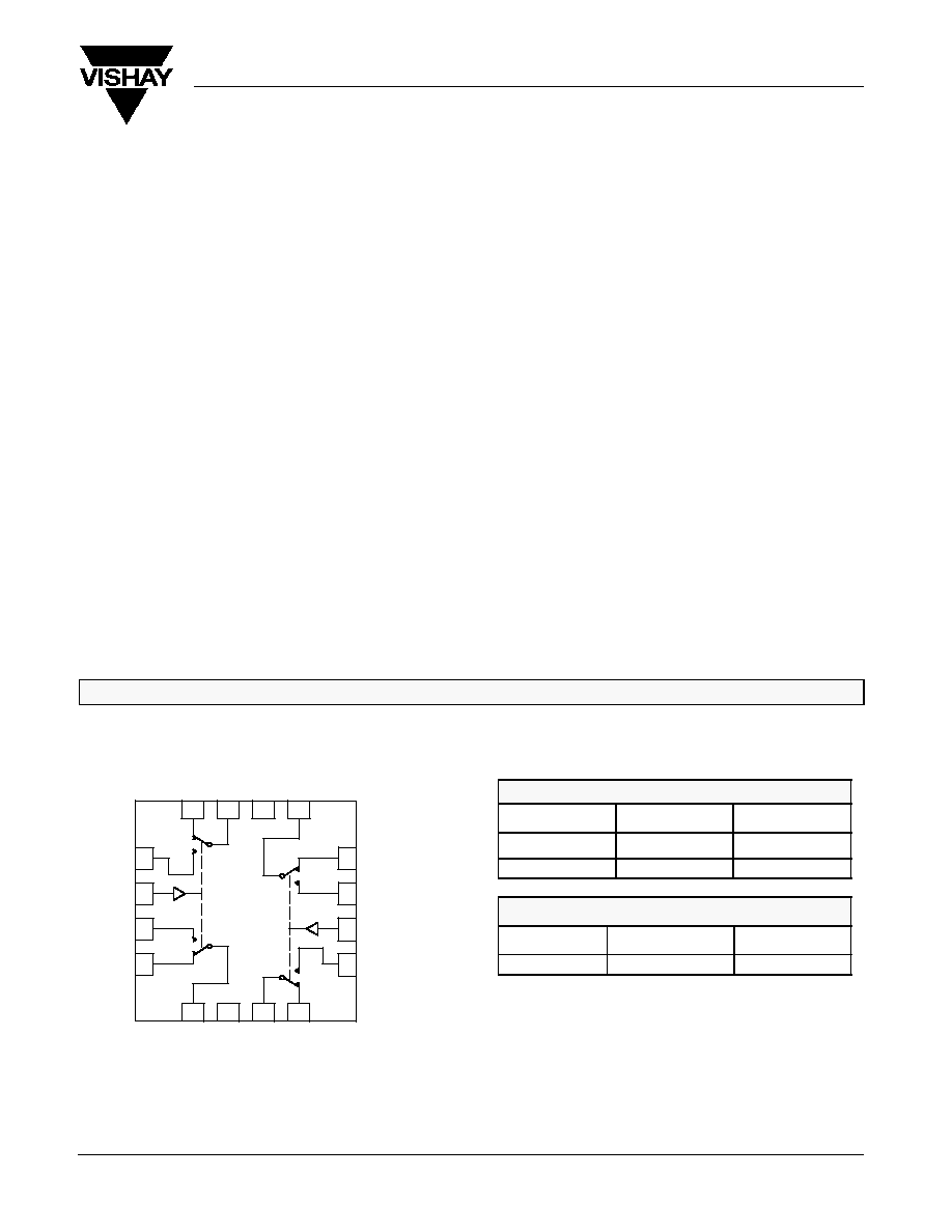
FUNCTIONAL BLOCK DIAGRAM AND PIN CONFIGURATION
TRUTH TABLE
Logic
NC1, 2, 3 and 4
NO1, 2, 3 and 4
0
ON
OFF
1
OFF
ON
ORDERING INFORMATION
Temp Range
Package
Part Number
-40 to 85
°
C
16-Pin QFN (4 x 4 mm)
DG2015DN
DG2015
Vishay Siliconix
New Product
www.vishay.com
2
Document Number: 71971
S-03423--Rev. B, 03-Mar-03
ABSOLUTE MAXIMUM RATINGS
Reference to GND
V+
-0.3 to +6 V
. . . . . . . . . . . . . . . . . . . . . . . . . . . . . . . . . . . . . . . . . . . . . . . . . . . .
IN, COM, NC, NO
a
-0.3 to (V+ + 0.3 V)
. . . . . . . . . . . . . . . . . . . . . . . . . . . . . . .
Current (Any terminal except NO, NC or COM)
30 mA
. . . . . . . . . . . . . . . . . .
Continuous Current (NO, NC, or COM)
"
150 mA
. . . . . . . . . . . . . . . . . . . . .
Peak Current
"
200 mA
. . . . . . . . . . . . . . . . . . . . . . . . . . . . . . . . . . . . . . . . . . . .
(Pulsed at 1 ms, 10% duty cycle)
Storage Temperature (D Suffix)
-65 to 150
°
C
. . . . . . . . . . . . . . . . . . . . . . . . . .
Package Solder Reflow Conditions
d
16-Pin QFN (4 x 4 mm)
240
°
C
. . . . . . . . . . . . . . . . . . . . . . . . . . . . . . . . . . . . . .
Power Dissipation (Packages)
b
QFN-16
c
1880 mW
. . . . . . . . . . . . . . . . . . . . . . . . . . . . . . . . . . . . . . . . . . . . . . .
Notes:
a.
Signals on NC, NO, or COM or IN exceeding V+ will be clamped by inter-
nal diodes. Limit forward diode current to maximum current ratings.
b.
All leads welded or soldered to PC Board.
c.
Derate 23.5 mW/
_
C above 70
_
C
d.
Manual soldering with iron is not recommended for leadless components.
The QFN is a leadless package. The end of the lead terminal is exposed
copper (not plated) as a result of the singulation process in manufactur-
ing. A solder fillet at the exposed copper lip cannot be guaranteed and is
not required to ensure adequate bottom side solder interconnection.
SPECIFICATIONS (V+ = 3 V)
Test Conditions
Otherwise Unless Specified
Limits
-40 to 85
_
C
Parameter
Symbol
V+ = 3 V,
"
10%, V
IN
= 0.4 or 2.0 V
e
Temp
a
Min
b
Typ
c
Max
b
Unit
Analog Switch
Analog Signal Range
d
V
NO
, V
NC
,
V
COM
Full
0
V+
V
On-Resistance
r
ON
V+ = 2.7 V, V
COM
= 0.2 V/1.5 V, I
NO
, I
NC
= 100 mA
Room
Full
0.85
1.6
1.7
r
ON
Flatness
r
ON
Flatness
V+ = 2.7 V
V
0 to V+ I
I 100 mA
Room
0.16
W
r
ON
Match
D
r
ON
V
COM
= 0 to V+, I
NO
, I
NC
= 100 mA
Room
0.15
Switch Off Leakage Current
I
NO(off)
,
I
NC(off)
V+ = 3.3 V, V
NO
, V
NC
= 1 V/3 V
Room
Full
-1
-10
1
10
Switch Off Leakage Current
I
COM(off)
V+ = 3.3 V, V
NO
, V
NC
= 1 V/3 V
V
COM
= 3 V/1 V
Room
Full
-1
-10
1
10
nA
Channel-On Leakage Current
I
COM(on)
V+ = 3.3 V, V
NO
, V
NC
= V
COM
= 1 V/3 V
Room
Full
-1
-10
1
10
Digital Control
Input High Voltage
V
INH
Full
2
V
Input Low Voltage
V
INL
Full
0.4
V
Input Capacitance
C
in
Full
4
pF
Input Current
I
INL
or I
INH
V
IN
= 0 or V+
Full
-1
1
m
A
Dynamic Characteristics
Turn-On Time
t
ON
Room
Full
40
65
67
Turn-Off Time
t
OFF
V
NO
or V
NC
= 2.0 V, R
L
= 300
W
, C
L
= 35 pF
Room
Full
35
60
62
ns
Break-Before-Make Time
t
d
Full
1
3
Charge Injection
d
Q
INJ
C
L
= 1 nF, V
GEN
= 0 V, R
GEN
= 0
W
Room
7
pC
Off-Isolation
d
OIRR
R
L
= 50
W
C
L
= 5 pF f = 1 MHz
Room
-67
dB
Crosstalk
d
X
TALK
R
L
= 50
W
, C
L
= 5 pF, f = 1 MHz
Room
-70
dB
N
O
N
C
Off Capacitance
d
C
NO(off)
Room
63
N
O
, N
C
Off Capacitance
d
C
NC(off)
V
IN
= 0 or V+ f = 1 MHz
Room
67
pF
Channel On Capacitance
d
C
NO(on)
V
IN
= 0 or V+, f = 1 MHz
Room
200
pF
Channel-On Capacitance
d
C
NC(on)
Room
196
DG2015
Vishay Siliconix
New Product
Document Number: 71971
S-03423--Rev. B, 03-Mar-03
www.vishay.com
3
SPECIFICATIONS (V+ = 3 V)
Parameter
Limits
-40 to 85
_
C
Temp
a
Test Conditions
Otherwise Unless Specified
Symbol
Parameter
Unit
Max
b
Typ
c
Min
b
Temp
a
V+ = 3 V,
"
10%, V
IN
= 0.4 or 2.0 V
e
Symbol
Power Supply
Power Supply Range
V+
2.7
3.3
V
Power Supply Current
I+
V
IN
= 0 or V+
Full
1.0
m
A
Power Consumption
P
C
V
IN
= 0 or V+
Full
3.3
m
W
Notes:
a.
Room = 25
°
C, Full = as determined by the operating suffix.
b.
Typical values are for design aid only, not guaranteed nor subject to production testing.
c.
The algebraic convention whereby the most negative value is a minimum and the most positive a maximum, is used in this data sheet.
d.
Guarantee by design, nor subjected to production test.
e.
V
IN
= input voltage to perform proper function.
f.
Guaranteed by 5-V leakage testing, not production tested.
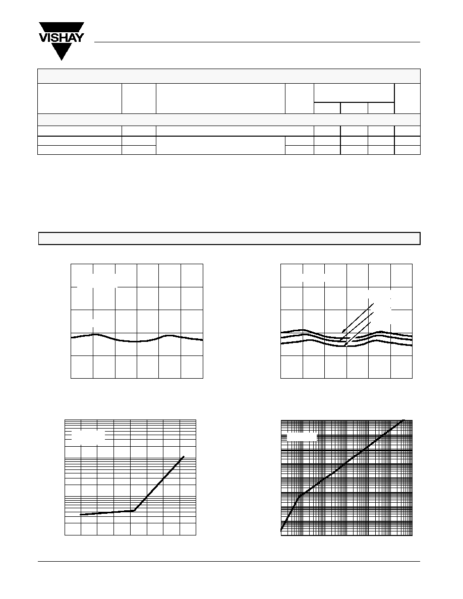
TYPICAL CHARACTERISTICS (25_C UNLESS NOTED)
10
10 K
100 K
10 M
100
1 K
1 M
10 mA
1 mA
100
m
A
10
m
A
1
m
A
10 nA
100 pA
-60
-40
-20
0
20
40
60
80
100
Supply Current vs. Input Switching Frequency
Input Switching Frequency (Hz)
I+
-
Supply Current (A)
0.0
0.5
1.0
1.5
2.0
2.5
0.0
0.5
1.0
1.5
2.0
2.5
3.0
r
ON
vs. V
COM
and Supply Voltage
V
COM
- Analog Voltage (V)
V+ = 3.0 V,
-
On-Resistance (
r
ON
W
)
0.0
0.5
1.0
1.5
2.0
2.5
0.0
0.5
1.0
1.5
2.0
2.5
3.0
r
ON
vs. Analog Voltage and Temperature
V
COM
- Analog Voltage (V)
25
_
C
-
On-Resistance (
r
ON
W
)
0.1
100
Supply Current vs. Temperature
V+ = 3 V
Temperature (
_
C)
1
10
I+
-
Supply Current (nA)
V+ = 3 V
T = 25
_
C
I
S
= 100 mA
-40
_
C
85
_
C
V+ = 3 V
V
IN
= 0 V
I
S
= 100 mA
100 nA
1 nA
DG2015
Vishay Siliconix
New Product
www.vishay.com
4
Document Number: 71971
S-03423--Rev. B, 03-Mar-03
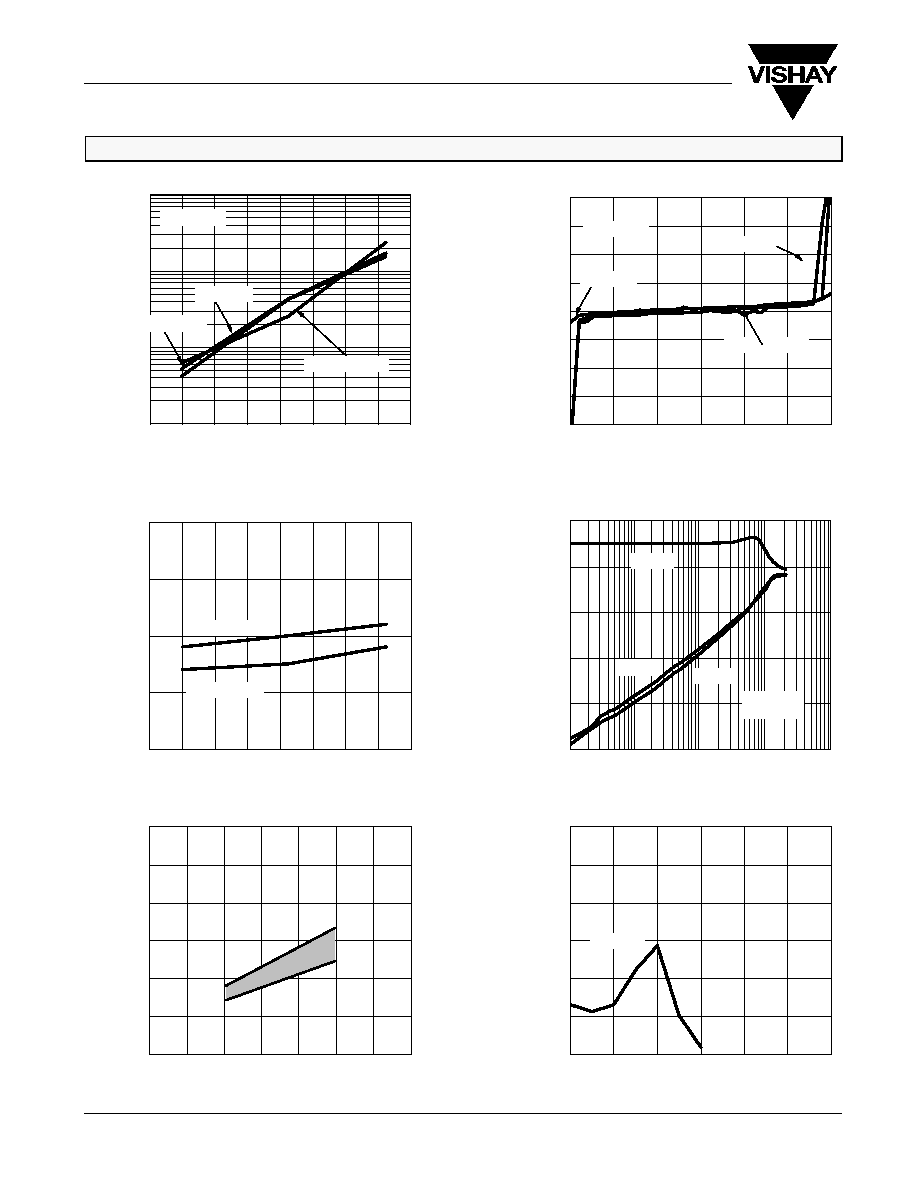
TYPICAL CHARACTERISTICS (25_C UNLESS NOTED)
-800
-600
-400
-200
0
200
400
600
800
0.0
0.5
1.0
1.5
2.0
2.5
3.0
Leakage vs. Analog Voltage
V
COM
, V
NO
, V
NC
- Analog Voltage (V)
-60
-40
-20
0
20
40
60
80
100
1
1000
Leakage Current vs. Temperature
Temperature (
_
C)
V+ = 3 V
10
100
Leakage Current (pA)
Leakage Current (pA)
V+ = 3 V
I
NO(off)
, II
NC(off)
I
COM(off)
I
COM(on)
I
NO(off)
, II
NC(off)
I
COM(on)
I
COM(off)
0.0
0.5
1.0
1.5
2.0
2.5
3.0
0
1
2
3
4
5
6
7
0
5
10
15
20
25
30
0
1
2
3
4
5
6
Charge Injection vs. Analog Voltage
V
COM
- Analog Voltage (V)
Q
-
Charge Injection (pC)
Switching Threshold vs. Supply Voltage
V+ - Supply Voltage (V)
-
Switching
Threshold (V)
V
T
100 K
-90
10 M
10
-70
-50
100 M
1 G
1 M
Insertion Loss, Off-Isolation
Crosstalk vs. Frequency
Frequency (Hz)
20
30
40
50
60
-60
-40
-20
0
20
40
60
80
100
Switching Time vs. Temperature
/
t
ON
-
Switching
T
ime (
t
OFF
s)
m
t
OFF
V+ = 3 V
(dB)
Loss, OIRR, X
T
ALK
-30
-10
V+ = 3 V
LOSS
OIRR
X
TALK
V+ = 3 V
R
L
= 50
W
Temperature (
_
C)
t
ON
V+ = 3 V
Leakage Current (pA)
DG2015
Vishay Siliconix
New Product
Document Number: 71971
S-03423--Rev. B, 03-Mar-03
www.vishay.com
5
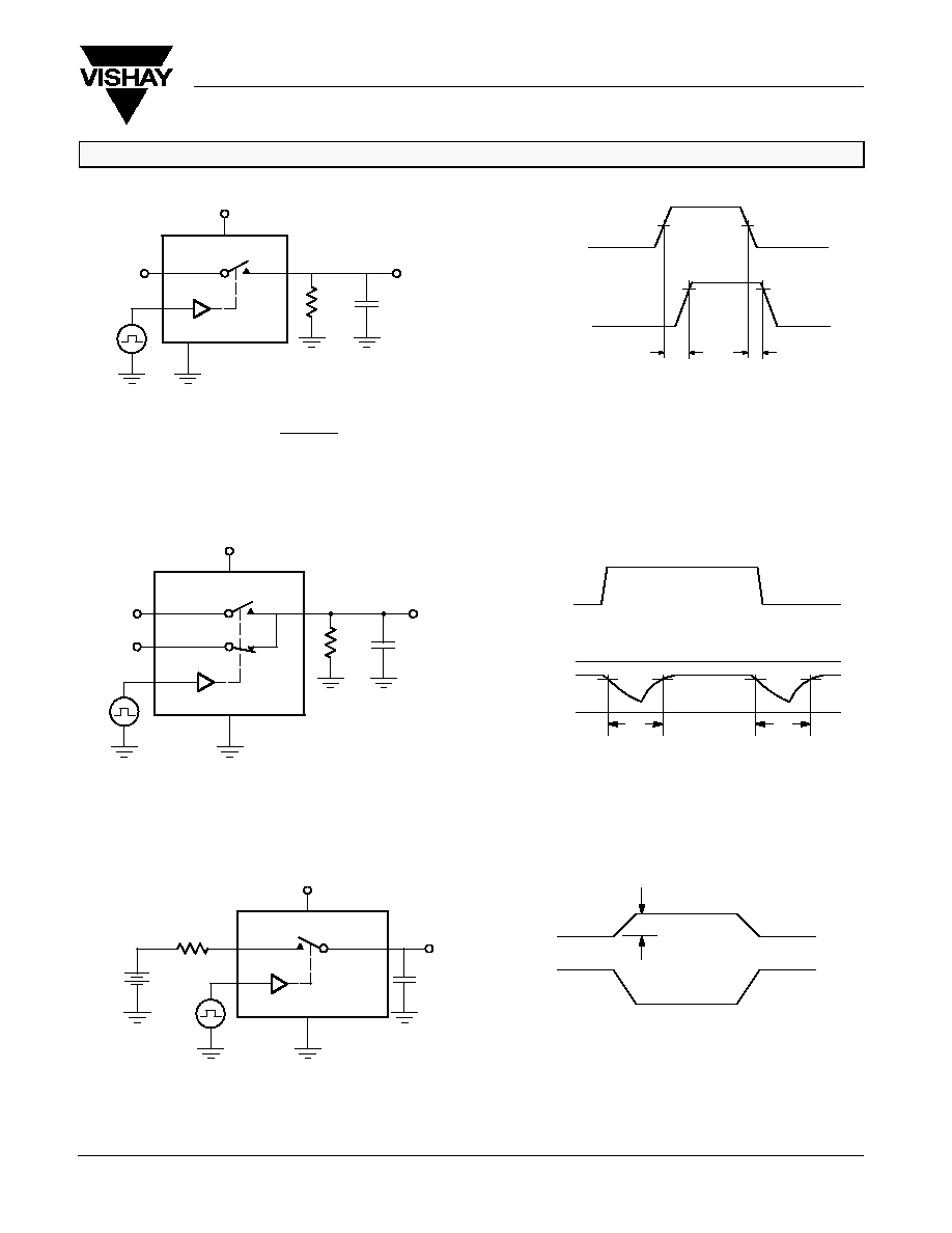
TEST CIRCUITS
Figure 1.
Switching Time
Switch
Input
C
L
(includes fixture and stray capacitance)
V+
IN
NO or NC
C
L
35 pF
COM
Logic
Input
R
L
300
W
V
OUT
GND
V+
50%
0 V
Logic
Input
Switch
Output
t
ON
t
OFF
Logic "1" = Switch On
Logic input waveforms inverted for switches that have
the opposite logic sense.
0 V
Switch Output
V
OUT
+
V
COM
R
L
R
L
)
R
ON
0.9 x V
OUT
t
r
t
5 ns
t
f
t
5 ns
V
INH
V
INL
Figure 3.
Charge Injection
Off
On
On
IN
D
V
OUT
V
OUT
Q =
D
V
OUT
x C
L
C
L
= 1 nF
R
gen
V
OUT
COM
V
IN
= 0 - V+
IN
V
gen
GND
V+
V+
IN depends on switch configuration: input polarity
determined by sense of switch.
+
NC or NO
Figure 2.
Break-Before-Make Interval
C
L
(includes fixture and stray capacitance)
NC
V
NO
NO
V
NC
0 V
Logic
Input
Switch
Output
V
O
V
NC
= V
NO
t
r
<5 ns
t
f
<5 ns
90%
t
D
t
D
IN
COM
V+
GND
V+
C
L
35 pF
V
O
R
L
300
W
V
INL
V
INH