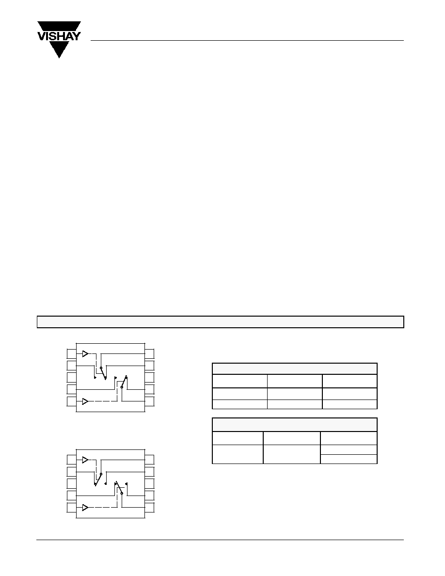
COM1
NC1
V+
1
2
3
10
9
Top View
IN1
NO1
GND
8
DG2016DQ--MSOP-10
NC2
COM2
4
5
7
NO2
IN2
6
COM1
NO1
V+
1
2
3
10
9
Top View
IN1
NC1
GND
8
DG2026DQ--MSOP-10
NO2
COM2
4
5
7
NC2
IN2
6
DG2016/DG2026
Vishay Siliconix
New Product
Document Number: 72030
S-31575--Rev. B, 11-Aug-03
www.vishay.com
1
High-Bandwidth, Low Voltage, Dual SPDT Analog Switchs
FEATURES
D
Single Supply (1.8 V to 5.5 V)
D
Low On-Resistance - r
ON:
2.4
W
D
Crosstalk and Off Isolation: -81 dB @
1 MHz
D
MSOP-10 Package
BENEFITS
D
Reduced Power Consumption
D
High Accuracy
D
Reduce Board Space
D
Low-Voltage Logic Compatible
D
High Bandwidth
APPLICATIONS
D
Cellular Phones
D
Speaker Headset Switching
D
Audio and Video Signal Routing
D
PCMCIA Cards
D
Low-Voltage Data Acquisition
D
ATE
DESCRIPTION
The DG2016/DG2026 are monolithic CMOS dual
single-pole/double-throw (SPDT) analog switchs. They are
specifically designed for low-voltage, high bandwidth
applications.
The DG2016/DG2026's on-resistance (3
W
@ 2.7 V),
matching and flatness are guaranteed over the entire analog
voltage range. Wide dynamic performance is achieved with
better than �80 dB for both cross-talk and off-isolation at
1 MHz.
Both SPDT's operate with independent control logic, conduct
equally well in both directions and block signals up to the
power supply level when off. Break-before-make is
guaranteed.
With fast switching speeds, low on-resistance, high
bandwidth, and low charge injection, the DG2016/DG2026 are
ideally suited for audio and video switching with high linearity.
Built on Vishay Siliconix's low voltage CMOS technology, the
DG2016/DG2026 contain an epitaxial layer which prevents
latch-up.
FUNCTIONAL BLOCK DIAGRAM AND PIN CONFIGURATION
TRUTH TABLE
Logic
NC1 and NC2
NO1 and NO2
0
ON
OFF
1
OFF
ON
ORDERING INFORMATION
Temp Range
Package
Part Number
40 to 85
�
C
MSOP 10
DG2016DQ
-40 to 85
�
C
MSOP-10
DG2026DQ
DG2016/DG2026
Vishay Siliconix
New Product
www.vishay.com
2
Document Number: 72030
S-31575--Rev. B, 11-Aug-03
ABSOLUTE MAXIMUM RATINGS
Reference to GND
V+
-0.3 to +6 V
. . . . . . . . . . . . . . . . . . . . . . . . . . . . . . . . . . . . . . . . . . . . . . . . . . . .
IN, COM, NC, NO
a
-0.3 to (V+ + 0.3 V)
. . . . . . . . . . . . . . . . . . . . . . . . . . . . . . . . . . . . . . .
Continuous Current (Any terminal)
"
50 mA
. . . . . . . . . . . . . . . . . . . . . . . . . . .
Peak Current
"
200 mA
. . . . . . . . . . . . . . . . . . . . . . . . . . . . . . . . . . . . . . . . . . . .
(Pulsed at 1 ms, 10% duty cycle)
Storage Temperature (D Suffix)
-65 to 150
�
C
. . . . . . . . . . . . . . . . . . . . . . . . . .
Power Dissipation (Packages)
b
MSOP-10
c
320 mW
. . . . . . . . . . . . . . . . . . . . . . . . . . . . . . . . . . . . . . . . . . . . . . .
Notes:
a.
Signals on NC, NO, or COM or IN exceeding V+ will be clamped by inter-
nal diodes. Limit forward diode current to maximum current ratings.
b.
All leads welded or soldered to PC Board.
c.
Derate 4.0 mW/
_
C above 70
_
C
SPECIFICATIONS (V+ = 3 V)
Test Conditions
Otherwise Unless Specified
Limits
-40 to 85
_
C
Parameter
Symbol
V+ = 3 V,
"
10%, V
IN
= 0.4 or 2.0 V
e
Temp
a
Min
b
Typ
c
Max
b
Unit
Analog Switch
Analog Signal Range
d
V
NO
, V
NC
,
V
COM
Full
0
V+
V
On-Resistance
r
ON
V+ = 2.7 V, V
COM
= 0.2 V/1.5 V
I
NO
, I
NC
= 10 mA
Room
Full
3.0
4.8
5.3
r
ON
Flatness
r
ON
Flatness
V+ = 2.7 V
V
0 to V+ I
I 10 mA
Room
1.6
W
r
ON
Match Between Channels
D
r
ON
V
COM
= 0 to V+, I
NO
, I
NC
= 10 mA
Room
0.2
Switch Off Leakage Current
f
I
NO(off)
,
I
NC(off)
V+ = 3.3 V, V
NO
, V
NC
= 0.3 V/3 V
Room
Full
-1
-10
1
10
Switch Off Leakage Current
f
I
COM(off)
V+ = 3.3 V, V
NO
, V
NC
= 0.3 V/3 V
V
COM
= 3 V/0.3 V
Room
Full
-1
-10
1
10
nA
Channel-On Leakage Current
f
I
COM(on)
V+ = 3.3 V, V
NO
, V
NC
= V
COM
= 0.3 V/3 V
Room
Full
-1
-10
1
10
Digital Control
Input High Voltage
d
V
INH
Full
1.6
V
Input Low Voltage
V
INL
Full
0.4
V
Input Capacitance
C
in
Full
5
pF
Input Current
I
INL
or I
INH
V
IN
= 0 or V+
Full
1
1
m
A
Dynamic Characteristics
Turn-On Time
t
ON
V
NO
or V
NC
= 2 0 V R
L
= 50
W
C
L
= 35 pF
Room
Full
28
53
59
Turn-Off Time
t
OFF
V
NO
or V
NC
= 2.0 V, R
L
= 50
W
, C
L
= 35 pF
Room
Full
13
38
38
ns
Break-Before-Make Time
t
d
V
NO
or V
NC
= 2.0 V, R
L
= 50
W
, C
L
= 35 pF
Full
1
Charge Injection
d
Q
INJ
C
L
= 1 nF, V
GEN
= 0 V, R
GEN
= 0
W
Room
38
pC
Off-Isolation
d
OIRR
R
L
= 50
W
C
L
= 5 pF f = 1 MHz
Room
-78
dB
Crosstalk
d
X
TALK
R
L
= 50
W
, C
L
= 5 pF, f = 1 MHz
Room
-82
dB
N
O
N
C
Off Capacitance
d
C
NO(off)
Room
15
N
O
, N
C
Off Capacitance
d
C
NC(off)
V
IN
= 0 or V+ f = 1 MHz
Room
15
pF
Channel On Capacitance
d
C
NO(on)
V
IN
= 0 or V+, f = 1 MHz
Room
49
pF
Channel-On Capacitance
d
C
NC(on)
Room
45
Power Supply
Power Supply Current
I+
V
IN
= 0 or V+
Full
0.01
1.0
m
A
Notes:
a.
Room = 25
�
C, Full = as determined by the operating suffix.
b.
Typical values are for design aid only, not guaranteed nor subject to production testing.
c.
The algebraic convention whereby the most negative value is a minimum and the most positive a maximum, is used in this data sheet.
d.
Guarantee by design, nor subjected to production test.
e.
V
IN
= input voltage to perform proper function.
f.
Guaranteed by 5-V leakage testing, not production tested.

DG2016/DG2026
Vishay Siliconix
New Product
Document Number: 72030
S-31575--Rev. B, 11-Aug-03
www.vishay.com
3
SPECIFICATIONS (V+ = 5 V)
Test Conditions
Otherwise Unless Specified
Limits
-40 to 85
_
C
Parameter
Symbol
V+ = 5 V,
"
10%, V
IN
= 0.8 or 2.4 V
e
Temp
a
Min
b
Typ
c
Max
b
Unit
Analog Switch
Analog Signal Range
d
V
NO
, V
NC
,
V
COM
Full
0
V+
V
On-Resistance
r
ON
V+ = 4.5 V, V
COM
= 3 V, I
NO
, I
NC
= 10 mA
Room
Full
2.4
4.0
4.3
r
ON
Flatness
r
ON
Flatness
V+ = 4.5 V, V
COM
= 0 to V+, I
NO
, I
NC
= 10 mA
Room
1.2
W
r
ON
Match Between Channels
D
r
ON
V+ = 4.5 V, V
COM
= 0 to V+, I
NO
, I
NC
= 10 mA
Room
0.2
Switch Off Leakage Current
I
NO(off)
,
I
NC(off)
V+ = 5.5 V
Room
Full
-1
-10
1
10
Switch Off Leakage Current
I
COM(off)
V+ = 5.5 V
V
NO
, V
NC
= 1 V/4.5 V, V
COM
= 4.5 V/1 V
Room
Full
-1
-10
1
10
nA
Channel-On Leakage Current
I
COM(on)
V+ = 5.5 V, V
NO
, V
NC
= V
COM
= 1 V/4.5 V
Room
Full
-1
-10
1
10
Digital Control
Input High Voltage
d
V
INH
Full
2.0
V
Input Low Voltage
V
INL
Full
0.8
V
Input Capacitance
C
in
Full
5
pF
Input Current
I
INL
or I
INH
V
IN
= 0 or V+
Full
1
1
m
A
Dynamic Characteristics
Turn-On Time
t
ON
V
NO
or V
NC
= 3 V R
L
= 50
W
C
L
= 35 pF
Room
Full
23
48
52
Turn-Off Time
t
OFF
V
NO
or V
NC
= 3 V, R
L
= 50
W
, C
L
= 35 pF
Room
Full
8
33
35
ns
Break-Before-Make Time
t
d
V
NO
or V
NC
= 3 V, R
L
= 50
W
, C
L
= 35 pF
Full
1
Charge Injection
d
Q
INJ
C
L
= 1 nF, V
GEN
= 0 V, R
GEN
= 0
W
Room
79
pC
Off-Isolation
d
OIRR
R
L
= 50
W
C
L
= 5 pF f = 1 MHz
Room
-81
dB
Crosstalk
d
X
TALK
R
L
= 50
W
, C
L
= 5 pF, f = 1 MHz
Room
-82
dB
Source Off Capacitance
d
C
NO(off)
Room
14
Source-Off Capacitance
d
C
NC(off)
V
IN
= 0 or V+ f = 1 MHz
Room
14
pF
Channel On Capacitance
d
C
NO(on)
V
IN
= 0 or V+, f = 1 MHz
Room
48
pF
Channel-On Capacitance
d
C
NC(on)
Room
44
Power Supply
Power Supply Range
V+
1.8
5.5
V
Power Supply Current
I+
V
IN
= 0 or V+
Full
0.01
1.0
m
A
Notes:
a.
Room = 25
�
C, Full = as determined by the operating suffix.
b.
Typical values are for design aid only, not guaranteed nor subject to production testing.
c.
The algebraic convention whereby the most negative value is a minimum and the most positive a maximum, is used in this data sheet.
d.
Guarantee by design, nor subjected to production test.
e.
V
IN
= input voltage to perform proper function.
f.
Guaranteed by 5-V leakage testing, not production tested.

DG2016/DG2026
Vishay Siliconix
New Product
www.vishay.com
4
Document Number: 72030
S-31575--Rev. B, 11-Aug-03
TYPICAL CHARACTERISTICS (25_C UNLESS NOTED)
-60
-40
-20
0
20
40
60
80
100
Supply Current vs. Input Switching Frequency
Input Switching Frequency (Hz)
I+
-
Supply Current (A)
0
1
2
3
4
5
6
7
8
0
1
2
3
4
5
r
ON
vs. V
COM
and Supply Voltage
V
COM
- Analog Voltage (V)
V+ = 3.0 V,
-
On-Resistance (
r
ON
W
)
0
1
2
3
4
5
0
1
2
3
4
5
r
ON
vs. Analog Voltage and Temperature
V
COM
- Analog Voltage (V)
25
_
C
-
On-Resistance (
r
ON
W
)
1
1000
10000
Supply Current vs. Temperature
-100
-75
-50
-25
0
25
50
75
100
0
1
2
3
4
5
Leakage vs. Analog Voltage
V
COM
, V
NO
, V
NC
- Analog Voltage (V)
V+ = 3 V
Temperature (
_
C)
V+ = 5 V
V
IN
= 0 V
10
100
I+
-
Supply Current (nA)
10
10 K
100 K
10 M
100
1 K
1 M
10 mA
1 mA
100
m
A
10
m
A
1
m
A
V+ = 5 V
T = 25
_
C
I
S
= 10 mA
V+ = 5.0 V,
-40
_
C
85
_
C
25
_
C
V+ = 5 V
-40
_
C
85
_
C
-60
-40
-20
0
20
40
60
80
100
1
1000
10000
Leakage Current vs. Temperature
Temperature (
_
C)
V+ = 5 V
10
100
Leakage Current (pA)
I
NO(off)
, II
NC(off)
I
COM(off)
I
COM(on)
Leakage Current (pA)
V+ = 5 V
I
NO(off)
, II
NC(off)
I
COM(off)
I
COM(on)
V+ = 3 V
V
IN
= 0 V
100 nA
10 nA

DG2016/DG2026
Vishay Siliconix
New Product
Document Number: 72030
S-31575--Rev. B, 11-Aug-03
www.vishay.com
5
TYPICAL CHARACTERISTICS (25_C UNLESS NOTED)
0.0
0.5
1.0
1.5
2.0
2.5
3.0
0
1
2
3
4
5
6
7
-80
-60
-40
-20
0
20
40
60
80
0
1
2
3
4
5
Charge Injection vs. Analog Voltage
V
COM
- Analog Voltage (V)
Q
-
Charge Injection (pC)
Switching Threshold vs. Supply Voltage
V+ - Supply Voltage (V)
-
Switching
Threshold (V)
V
T
100 K
-90
10 M
10
-70
-50
100 M
1 G
1 M
Insertion Loss, Off-Isolation
Crosstalk vs. Frequency
Frequency (Hz)
0
10
20
30
40
50
60
-60
-40
-20
0
20
40
60
80
100
Switching Time vs. Temperature
R
L
= 50
W
/
t
ON
-
Switching
T
ime (
t
OFF
s)
m
t
ON
V+ = 5 V
t
OFF
V+ = 5 V
t
OFF
V+ = 3 V
(dB)
Loss, OIRR, X
T
ALK
-30
-10
V+ = 5 V
V+ = 3 V
LOSS
OIRR
X
TALK
V+ = 5 V
R
L
= 50
W
Temperature (
_
C)
t
ON
V+ = 3 V
TEST CIRCUITS
FIGURE 1. Switching Time
Switch
Input
C
L
(includes fixture and stray capacitance)
V+
IN
NO or NC
C
L
35 pF
COM
Logic
Input
R
L
50
W
V
OUT
GND
V+
50%
0 V
Logic
Input
Switch
Output
t
ON
t
OFF
Logic "1" = Switch On
Logic input waveforms inverted for switches that have
the opposite logic sense.
0 V
Switch Output
V
OUT
+
V
COM
R
L
R
L
)
R
ON
0.9 x V
OUT
t
r
t
5 ns
t
f
t
5 ns
V
INH
V
INL