/home/web/doc/html/vishay/153736
DG2715/DG2716
Vishay Siliconix
New Product
Document Number: 72740
s-42443--Rev. A, 10-jAN-05
www.vishay.com
1
Low-Voltage, 0.4-
W
r
ON
, Single SPST Analog Switch
FEATURES
D Low Voltage Operation (1.6 V to 3.6 V)
D Low On-Resistance - r
DS(on)
:
0.4 W @ 2.7 V
D Off-Isolation: -57 dB @ 1 MHz
D Fast Switching: 25 ns t
ON
D Low Charge Injection--Q
INJ
: 9 pC
D Low Power Consumption: t1 mW
D SC-70 5-Lead Package
BENEFITS
D High Accuracy
D High Bandwidth
D TTL and Low Voltage Logic
Compatibility
D Low Power Consumption
D Reduced PCB Space
APPLICATIONS
D Mixed Signal Routing
D Portable and Battery Operated
Systems
D Low Voltage Data Acquisition
D Modems
D PCMCIA Cards
DESCRIPTION
The DG2715/2716 are low voltage, single supply, dual SPST
analog switches. Designed for high performance switching of
analog signals, the DG2715/2716 provide low on-resistance
(0.4 @ +2.7 V), fast speed (t
ON
, t
OFF
@ 17 ns and 14 ns)
and the ability to handle signals over the entire analog voltage
range.
When operated on a +3-V supply, control pins are compatible
with 1.8-V digital logic. Additionally, on-resistance flatness and
matching (0.05 and 0.1 ) offer high accuracy between
channels.
Built on Vishay Siliconix's low voltage submicron CMOS
process, the DG2715/16 were designed to offer solutions that
extend beyond audio/video functions, to providing the
performance required for today's demanding mixed-signal
switching in portable applications.
The DG2715 contains a normally open (NO) switch, and the
DG2716 contains a normally closed switch. An epitaxial layer
prevents latch-up. All switches conduct equally well in both
directions when on, and block up to the power supply level
when off.
As a committed partner to the community and the
environment, Vishay Siliconix manufactures this product with
the lead (Pb)-free device terminations. For analog switching
products manufactured with 100% matte tin device
terminations, the lead (Pb)-free "--E3" suffix is being used as
a designator.
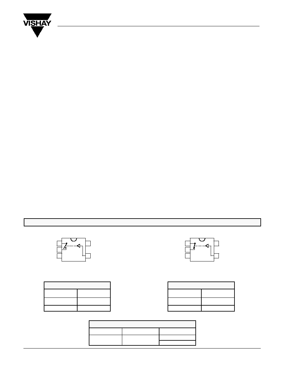
FUNCTIONAL BLOCK DIAGRAM AND PIN CONFIGURATION
V+
IN
1
2
3
5
Top View
COM
NO
GND
4
SC-70-5L
Device Marking: F7
DG2715
V+
IN
1
2
3
5
Top View
COM
NC
GND
4
SC-70-5L
Device Marking: F6
DG2716
TRUTH TABLE-DG2715
Logic
Switch
0
OFF
1
ON
TRUTH TABLE-DG2716
Logic
Switch
0
ON
1
OFF
ORDERING INFORMATION
Temp Range
Package
Part Number
40 to 85�C
SC70 5
DG2715DL-T1--E3
-40 to 85�C
SC70-5
DG2716DL-T1--E3
DG2715/DG2716
Vishay Siliconix
New Product
www.vishay.com
2
Document Number: 72740
s-42443--Rev. A, 10-jAN-05
ABSOLUTE MAXIMUM RATINGS
Reference to GND
V+
-0.3 to 4 V
. . . . . . . . . . . . . . . . . . . . . . . . . . . . . . . . . . . . . . . . . . . . . . . . . . . . . .
IN, COM, NC, NO
a
-0.3 to (V+ + 0.3 V)
. . . . . . . . . . . . . . . . . . . . . . . . . . . . . . . . . . . . . . .
Continuous Current (NO, NC and COM Pins)
"200 mA
. . . . . . . . . . . . . . . . .
Peak Current
"300 mA
. . . . . . . . . . . . . . . . . . . . . . . . . . . . . . . . . . . . . . . . . . . .
(Pulsed at 1 ms, 10% duty cycle)
Storage Temperature (D Suffix)
-65 to 150�C
. . . . . . . . . . . . . . . . . . . . . . . . . . .
Power Dissipation (Packages)
b
5-Pin SC-70
c
250 mW
. . . . . . . . . . . . . . . . . . . . . . . . . . . . . . . . . . . . . . . . . . . . . .
Notes:
a.
Signals on NC, NO, or COM or IN exceeding V+ will be clamped by
internal diodes. Limit forward diode current to maximum current ratings.
b.
All leads welded or soldered to PC Board.
c.
Derate 3.1 mW/_C above 70_C
Stresses beyond those listed under "Absolute Maximum Ratings" may cause permanent damage to the device. These are stress ratings only, and functional operation
of the device at these or any other conditions beyond those indicated in the operational sections of the specifications is not implied. Exposure to absolute maximum
rating conditions for extended periods may affect device reliability.
SPECIFICATIONS (V+ = 1.8 V)
Test Conditions
Otherwise Unless Specified
Limits
-40 to 85_C
Parameter
Symbol
V+ = 1.8 V, "10%, V
IN
= 0.4 or 1.0 V
e
Temp
a
Min
b
Typ
c
Max
b
Unit
Analog Switch
Analog Signal Range
d
V
NO
, V
NC
,
V
COM
Full
0
V+
V
On-Resistance
r
ON
V+ = 1.8 V, V
COM
= 0.9 V
I
NO
, I
NC
= 10 mA
Room
Full
d
0.7
1.5
2.0
W
Switch Off Leakage Current
f
I
NO(off),
I
NC(off)
V+ = 2.0 V
Room
Full
d
-1
-10
1
10
Switch Off Leakage Current
f
I
COM(off)
V+ = 2.0 V
V
NO,
V
NC
= 0.2 V/1.8 V, V
COM
= 1.8 V/0.2 V
Room
Full
d
-1
-10
1
10
nA
Channel-On Leakage Current
f
I
COM(on)
V+ = 2.0 V, V
NO,
V
NC
= V
COM
= 0.2 V/1.8 V
Room
Full
d
-1
-10
1
10
Digital Control
Input High Voltage
V
INH
Full
1.0
V
Input Low Voltage
V
INL
Full
0.4
V
Input Capacitance
d
C
in
Full
4
pF
Input Current
f
I
INL
or I
INH
V
IN
= 0 or V+
Full
-1
1
mA
Dynamic Characteristics
Turn-On Time
d
t
ON
V
NO
or V
NC
= 1.5 V, R
L
= 50 W, C
L
= 35 pF
Room
Full
d
24
36
ns
Turn-Off Time
d
t
OFF
V
NO
or V
NC
= 1.5 V, R
L
= 50 W, C
L
= 35 pF
Figures 1 and 2
Room
Full
d
21
33
ns
Charge Injection
d
Q
INJ
C
L
= 1 nF, V
GEN
= 0 V, R
GEN
= 0 W, Figure 3
Room
13
pC
Off-Isolation
d
OIRR
R
L
= 50 W, C
L
= 5 pF, f = 1 MHz
Room
-57
dB
NO, NC Off Capacitance
d
C
NO(off),
C
NC(off)
V
IN
= 0 or V+, f = 1 MHz
Room
78
pF
Channel-On Capacitance
d
C
ON
V
IN
= 0 or V+, f = 1 MHz
Room
93
pF
DG2715/DG2716
Vishay Siliconix
New Product
Document Number: 72740
s-42443--Rev. A, 10-jAN-05
www.vishay.com
3
SPECIFICATIONS (V+ = 3.0 V)
Test Conditions
Otherwise Unless Specified
Limits
-40 to 85_C
Parameter
Symbol
V+ = 3 V, "10%, V
IN
= 0.5 or 1.4 V
e
Temp
a
Min
b
Typ
c
Max
b
Unit
Analog Switch
Analog Signal Range
d
V
NO
, V
NC
,
V
COM
Full
0
V+
V
On-Resistance
r
ON
V+ = 2.7 V, V
COM
= 1.5 V, I
NO
I
NC
= 100 mA
Room
Full
0.4
0.6
W
r
ON
Flatness
r
ON
Flatness
V+ = 2.7 V, V
COM
= 0 .6 V, 1.5 V, 2.1 V
I
NO
, I
NC
= 100 mA
Room
0.1
0.2
W
Switch Off Leakage Current
I
NO(off),
I
NC(off)
V+ = 3.3 V
Room
Full
-1
-10
1
10
Switch Off Leakage Current
I
COM(off)
V+ = 3.3 V
V
NO,
V
NC
= 0.3 V/3 V, V
COM
= 3 V/0.3 V
Room
Full
-1
-10
1
10
nA
Channel-On Leakage Current
I
COM(on)
V+ = 3.3 V, V
NO,
V
NC
= V
COM
= 0.3 V/3 V
Room
Full
-1
-10
1
10
Digital Control
Input High Voltage
V
INH
Full
1.4
V
Input Low Voltage
V
INL
Full
0.5
V
Input Capacitance
d
C
in
Full
5
pF
Input Current
I
INL
or I
INH
V
IN
= 0 or V+
Full
-1
1
mA
Dynamic Characteristics
Turn-On Time
t
ON
V
NO
or V
NC
= 1.5 V, R
L
= 50 W, C
L
= 35 pF
Room
Full
17
29
ns
Turn-Off Time
t
OFF
V
NO
or V
NC
= 1.5 V, R
L
= 50 W, C
L
= 35 pF
Figure 1
Room
Full
14
26
ns
Charge Injection
d
Q
INJ
C
L
= 1 nF, V
GEN
= 0 V, R
GEN
= 0 W, Figure 3
Room
9
pC
Off-Isolation
d
OIRR
R
L
= 50 W, C
L
= 5 pF, f = 1 MHz
Room
-57
dB
NO, NC Off Capacitance
d
C
NO(off),
C
NC(off)
V
IN
= 0 or V+, f = 1 MHz
Room
72
pF
Channel-On Capacitance
d
C
ON
V
IN
= 0 or V+, f = 1 MHz
Room
92
pF
Power Supply
Power Supply Range
V+
1.5
3.6
V
Power Supply Current
I+
V+ = 3.6 V, V
IN
= 0 or V+
0.01
1.0
mA
Notes:
a.
Room = 25�C, Full = as determined by the operating suffix.
b.
The algebraic convention whereby the most negative value is a minimum and the most positive a maximum, is used in this data sheet.
c.
Typical values are for design aid only, not guaranteed nor subject to production testing.
d.
Guarantee by design, nor subjected to production test.
e.
V
IN
= input voltage to perform proper function.
f.
Guaranteed by 3-V leakage testing, not production tested.
DG2715/DG2716
Vishay Siliconix
New Product
www.vishay.com
4
Document Number: 72740
s-42443--Rev. A, 10-jAN-05
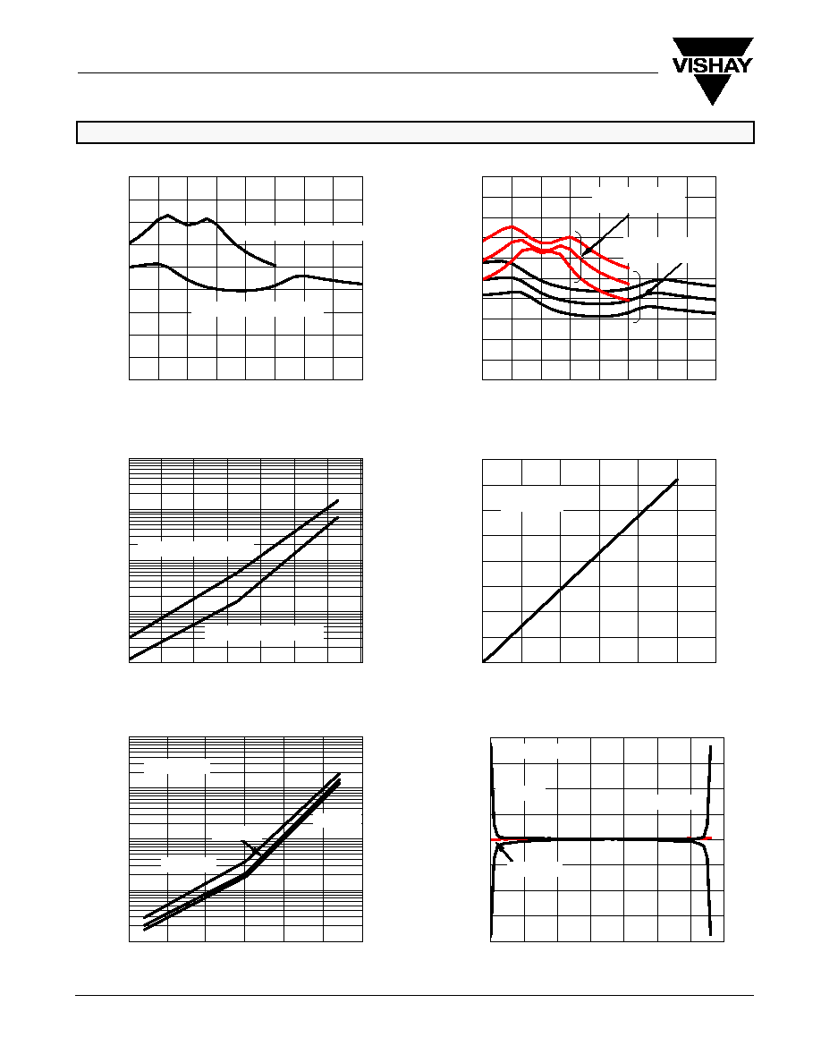
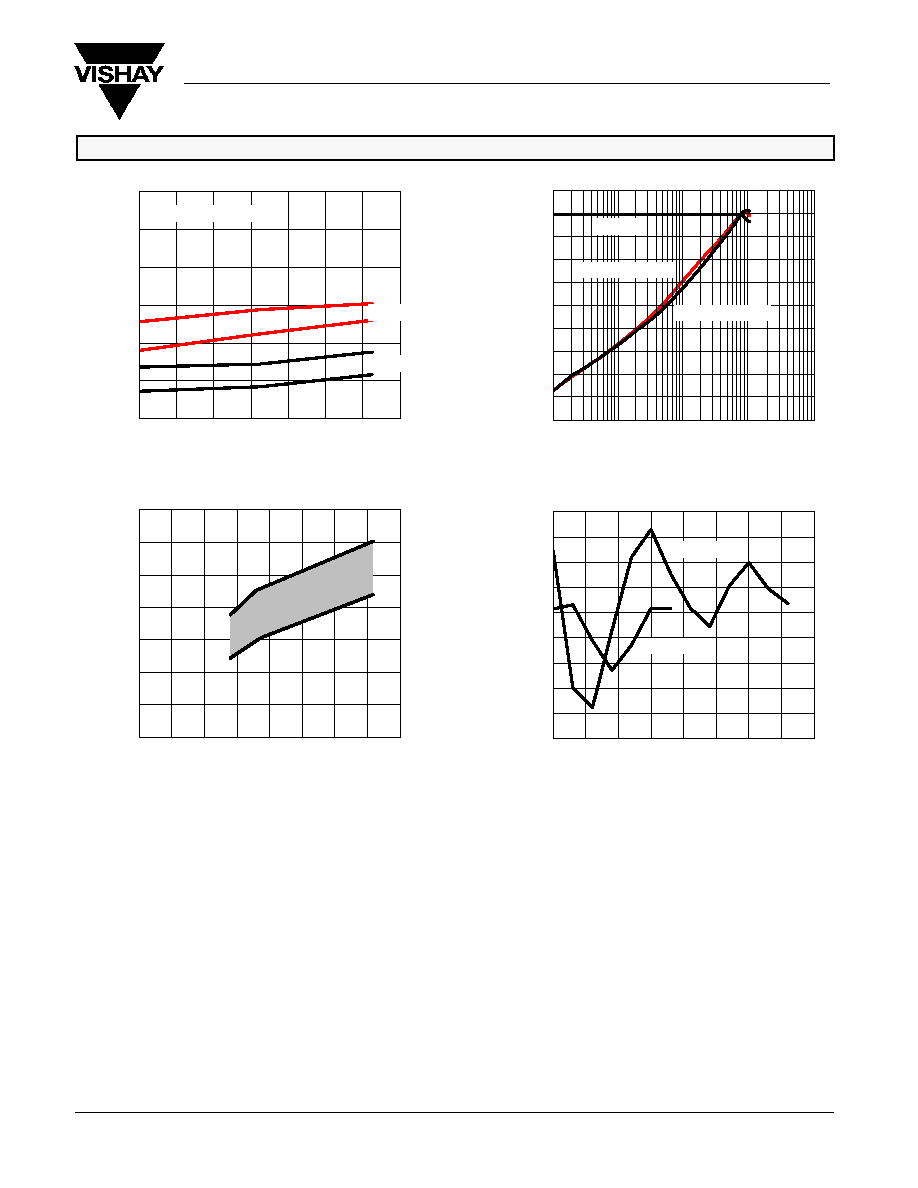
TYPICAL CHARACTERISTICS (25_C UNLESS NOTED)
-2000
-1500
-1000
-500
0
500
1000
1500
2000
0.0
0.5
1.0
1.5
2.0
2.5
3.0
3.5
-40
-20
0
20
40
60
80
100
-50
-25
0
25
50
75
100
1
100
10,000
100
1
Supply Current vs. Temperature
Temperature (_C)
0.0
0.1
0.2
0.3
0.4
0.5
0.6
0.7
0.8
0.9
1.0
0.3
0.6
0.9
1.2
1.5
1.8
2.1
2.4
2.7
0.0
0.1
0.2
0.3
0.4
0.5
0.6
0.7
0.8
0.9
0.3
0.6
0.9
1.2
1.5
1.8
2.1
2.4
2.7
Leakage Current vs. Temperature
Leakage Current vs. Analog Voltage
r
DS(on)
vs. V
COM
vs. 1 V
CC
V
D
(V)
r
DS(on)
vs. V
D
, V
CC
and Temperature
10
V
SUP
= 3.6 V, V
IN
= 0 V
Leakage Current (pA)
Temperature (_C)
10000
10
I
NO/NC(off)
Leakage Current (pA)
V+ = 3.3 V
V
CC
= 1.8 V
85, 25 and -40 _C
1000
V+ = 3.3 V
r
DS(on)
(
W
)
V+ = 1.8 V, I
NO/NC
= 10 mA
r
DS(on)
(
W
)
V
D
(V)
I
CC
Supply Current (pA)
1000
I
COM(off)
I
COM(on)
V
COM
, V
NO
, V
NC
- Analog Voltage (V)
Inout Switching Frequency (kHz)
0
500
1000
1500
2000
2500
3000
3500
4000
0
2000
4000
6000
8000
10000
12000
Switching Frequency vs. Supply Current
Power
Supply Current (
m
A)
V+ = 2.7 V, I
NO/NC
= 100 mA
V+ = 3.6 V
V
IN
= 3.6 V
I
COM(on)
I
COM(off)
I
NO/NC(off)
V
CC
= 2.7 V
85, 25 and -40 _C
V
SUP
= 3.6 V, V
IN
= 3.6 V
DG2715/DG2716
Vishay Siliconix
New Product
Document Number: 72740
s-42443--Rev. A, 10-jAN-05
www.vishay.com
5
TYPICAL CHARACTERISTICS (25_C UNLESS NOTED)
10
15
20
25
30
35
40
-40
-20
0
20
40
60
80
100
Switching Time vs. V
CC
, and Temperature
Temperature (_C)
t
ON
,
t
OFF
-
Switching
T
ime (ns)
0.0
0.2
0.4
0.6
0.8
1.0
1.2
1.4
0.0
0.5
1.0
1.5
2.0
2.5
3.0
3.5
4.0
V
SUPPLY
(v)
Input V
oltage (V)
Threshold vs. Supply Voltage
R
L
= 50 W, C
L
= 35 pF
V
CC
= 1.8 V
-90
-20
10
Insertion Loss, Off-Isolation vs. Frequency
Frequency (kHz)
-10
0
10 K
1 M
100 K
1 K
10 0
-30
-40
-50
-60
-70
-80
OIRR, V+ = 3.6 V
LOSS, OIRR (dB)
OIRR, V+ = 1.8 V
LOSS
V
CC
= 3.0 V
-50
-40
-30
-20
-10
0
10
20
30
40
0.0
0.5
1.0
1.5
2.0
2.5
3.0
3.5
4.0
V
COM
- Analog Voltage (v)
Q
-
Charge Injection (pC)
Charge Injection vs. Analog Voltage
V+ = 3.6 V
V+ = 1.8 V
Document Outline