DG3001/3002/3003
Vishay Siliconix
New Product
Document Number: 72505
S-32069--Rev. A, 27-Oct-03
www.vishay.com
1
Low-Voltage Sub-Ohm SPST/SPDT MICRO FOOTr Analog Switch
FEATURES
D MICRO FOOT Chip Scale Package
(1.0 x 1.5 mm)
D Low Voltage Operation (1.8 V to 5.5 V)
D Low On-Resistance - r
DS(on
): 0.4 W
D Fast Switching - t
ON
: 47 ns, t
OFF
: 40 ns
D Low Power Consumption
D TTL/CMOS Compatible
BENEFITS
D Reduced Power Consumption
D Simple Logic Interface
D High Accuracy
D Reduce Board Space
APPLICATIONS
D Cellular Phones
D Communication Systems
D Portable Test Equipment
D Battery Operated Systems
D PCM Cards
D PDA
DESCRIPTION
The DG3001/DG3002/DG3003 are monolithic CMOS analog
switches designed for high performance switching of analog
signals. The DG3001 and DG3002 are configured as SPST
switches, and the DG3003 is an SPDT switch. Combining low
power, high speed (t
ON
: 47 ns, t
OFF
: 40 ns), low on-resistance
(r
DS(on)
: 0.4 W) and small physical size (MICRO FOOT,
6-bump), the DG3001/DG3002/DG3003 are ideal for portable
and battery powered applications requiring high performance
and efficient use of board space.
The DG3001/DG3002/DG3003 are built on Vishay Siliconix's
low voltage JI2 process. An epitaxial layer prevents latchup.
Each switch conducts equally well in both directions when on,
and blocks up to the power supply level when off.
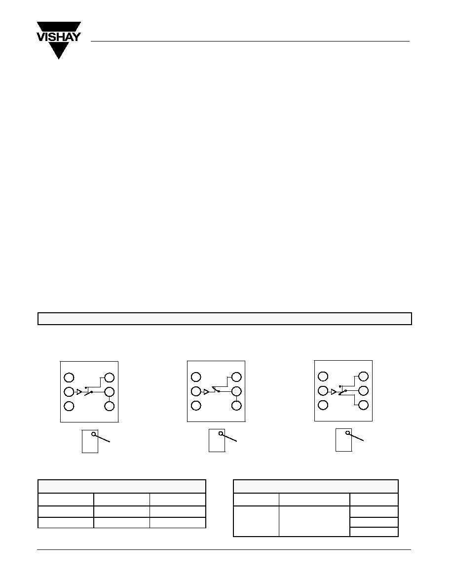
FUNCTIONAL BLOCK DIAGRAM AND PIN CONFIGURATION
NO
(Source
1
)
COM
COM
B1
B2
B3
Top View
V+
IN
GND
A1
A2
A3
XXX
3001
Device Marking: 3001
xxx = Date/Lot Traceability Code
A1 Locator
NC
(Source
1
)
COM
COM
B1
B2
B3
Top View
V+
IN
GND
A1
A2
A3
XXX
3002
Device Marking: 3002
xxx = Date/Lot Traceability Code
A1 Locator
NO
(Source
1
)
COM
NC (Source
2
)
B1
B2
B3
Top View
V+
IN
GND
A1
A2
A3
XXX
3003
Device Marking: 3003
xxx = Date/Lot Traceability Code
A1 Locator
DG3001DB
DG3002DB
DG3003DB
MICRO FOOT (6-Bump)
MICRO FOOT (6-Bump)
MICRO FOOT (6-Bump)
TRUTH TABLE
Logic
NC
NO
0
ON
OFF
1
OFF
ON
ORDERING INFORMATION
Temp Range
Package
Part Number
MICRO FOOT: 6-Bump
DG3001DB
-40 to 85�C
MICRO FOOT: 6-Bump
(3 2, 0.5-mm pitch,
165 mm nom bump height)
DG3002DB
165-mm nom. bump height)
DG3003DB
DG3001/3002/3003
Vishay Siliconix
New Product
www.vishay.com
2
Document Number: 72505
S-32069--Rev. A, 27-Oct-03
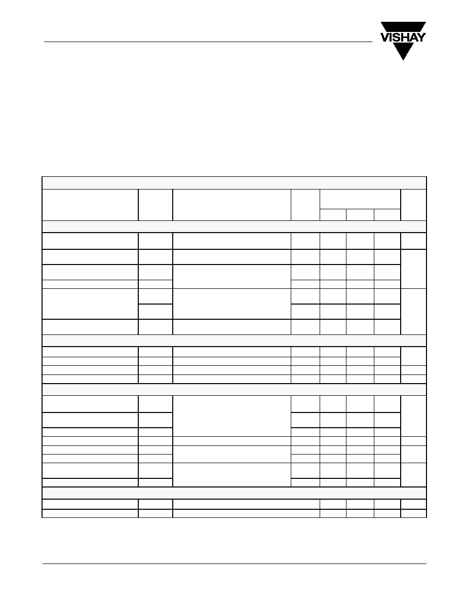
ABSOLUTE MAXIMUM RATINGS
Reference to GND
V+
-0.3 to +6 V
. . . . . . . . . . . . . . . . . . . . . . . . . . . . . . . . . . . . . . . . . . . . . . . . . . . .
IN, COM, NC, NO
a
-0.3 to (V+ + 0.3 V)
. . . . . . . . . . . . . . . . . . . . . . . . . . . . . . . . . . . . . . .
Continuous Current (NO, NC, COM)
"250 mA
. . . . . . . . . . . . . . . . . . . . . . . .
Peak Current
"400 mA
. . . . . . . . . . . . . . . . . . . . . . . . . . . . . . . . . . . . . . . . . . . . .
(Pulsed at 1 ms, 10% duty cycle)
Storage Temperature (D Suffix)
-65 to 150�C
. . . . . . . . . . . . . . . . . . . . . . . . . . . .
Package Reflow Conditions
b
VPR
215�C
. . . . . . . . . . . . . . . . . . . . . . . . . . . . . . . . . . . . . . . . . . . . . . . . . . . . . . . .
IR/Convection
220�C
. . . . . . . . . . . . . . . . . . . . . . . . . . . . . . . . . . . . . . . . . . . . . . .
Power Dissipation (Packages)
c
6-Bump, 2 x 3 MICRO FOOT
d
250 mW
. . . . . . . . . . . . . . . . . . . . . . . . . . . . . . .
Notes:
a
Signals on NC, NO, or COM or IN exceeding V+ will be clamped by
internal diodes. Limit forward diode current to maximum current ratings.
b
Refer to IPC/JEDEC (J-STD-020A)
c
All bumps soldered to PC Board.
d
Derate 3.1 mW/_C above 70_C
SPECIFICATIONS (V+ = 3.0 V)
Test Conditions
Otherwise Unless Specified
Limits
-40 to 85_C
Parameter
Symbol
V+ = 3 V, "10%, V
IN
= 0.4 or 2.0 V
e
Temp
a
Min
b
Typ
c
Max
b
Unit
Analog Switch
Analog Signal Range
d
V
NO
, V
NC
,
V
COM
Full
0
V+
V
On-Resistance
d
r
ON
V+ = 2.7 V, V
COM
= 1.5 V, I
NO
, I
NC
= 10 mA
Room
Full
0.4
0.7
0.8
r
ON
Flatness
d
r
ON
Flatness
V+ = 2.7 V, V
COM
= 0 to V+, I
NO
, I
NC
= 10 mA
Room
0.1
0.2
W
r
ON
Match
d
Dr
ON
V+ = 2.7 V, V
COM
= 0 to V+, I
NO
, I
NC
= 10 mA
Room
0.01
0.05
Switch Off Leakage Current
f
I
NO(off),
I
NC(off)
V+ = 3.3 V
Room
Full
1
-10
1
10
Switch Off Leakage Current
f
I
COM(off)
V+ = 3.3 V
V
NO,
V
NC
= 0.3 V/3 V, V
COM
= 3 V/0.3 V
Room
Full
1
-10
1
10
nA
Channel-On Leakage Current
f
I
COM(on)
V+ = 3.3 V, V
NO,
V
NC
= V
COM
= 0.3 V/3 V
Room
Full
1
-10
1
10
Digital Control
Input High Voltage
V
INH
Full
2
V
Input Low Voltage
V
INL
Full
0.4
V
Input Capacitance
d
C
in
Full
5
pF
Input Current
d
I
INL
or I
INH
V
IN
= 0 or V+
Full
-1
1
mA
Dynamic Characteristics
Turn-On Time
d
t
ON
V
or V 2 0 V R 300 W C 35 pF
Room
Full
47
71
Turn-Off Time
d
t
OFF
V
NO
or V
NC
= 2.0 V, R
L
= 300 W, C
L
= 35 pF
Figure 1 and 2
Room
Full
40
59
ns
Break-Before-Make Time
d
t
d
Room
1
6
Charge Injection
d
Q
INJ
C
L
= 1 nF, V
GEN
= 0 V, R
GEN
= 0 W, Figure 3
Room
64
pC
Off-Isolation
d
OIRR
R
L
= 50 W C
L
= 5 pF f = 100 kHz
Room
-70
dB
Crosstalk
d
X
TALK
R
L
= 50 W, C
L
= 5 pF, f = 100 kHz
Room
-70
dB
NO, NC Off Capacitance
d
C
NO(off),
C
NC(off)
V
IN
= 0 or V+, f = 1 MHz
Room
100
pF
Channel-On Capacitance
d
C
ON
V
IN
= 0 or V+, f = 1 MHz
Room
340
pF
Power Supply
Power Supply Range
V+
2.7
3.3
V
Power Supply Current
d
I+
V
IN
= 0 or V+
0.1
1.0
mA
Notes:
a.
Room = 25�C, Full = as determined by the operating suffix.
b.
The algebraic convention whereby the most negative value is a minimum and the most positive a maximum, is used in this data sheet.
c.
Typical values are for design aid only, not guaranteed nor subject to production testing.
d.
Guarantee by design, nor subjected to production test.
e.
V
IN
= input voltage to perform proper function.

DG3001/3002/3003
Vishay Siliconix
New Product
Document Number: 72505
S-32069--Rev. A, 27-Oct-03
www.vishay.com
3
TYPICAL CHARACTERISTICS (25_C UNLESS NOTED)
-60
-40
-20
0
20
40
60
80
100
10000
1000
1
Supply Current vs. Temperature
Temperature (_C)
I+
-
Supply Current (nA)
-
On-Resistance (
r
ON
W
)
0.00
0.20
0.40
0.60
0.80
1.00
0.0
0.5
1.0
1.5
2.0
2.5
3.0
0.00
0.25
0.50
0.75
1.00
1.25
1.50
1.75
2.00
0
1
2
3
4
5
r
ON
vs. V
COM
and Single Supply Voltage
V
COM
- Analog Voltage (V)
V+ = 1.8 V
V+ = 2 V
V+ = 5 V
r
ON
vs. Analog Voltage and Temperature
-
On-Resistance (
r
ON
W
)
V
COM
- Analog Voltage (V)
85_C
-40_C
25_C
10
V+ = 5 V
V
IN
= 0 V
T = 25 _C
I
S
= 10 mA
V+ = 2.7 V
V+ = 3 V
V+ = 3.3 V
V+ = 3 V
I
S
= 10 mA
100
Supply Current vs. Input Switching Frequency
Input Switching Frequency (Hz)
I+
-
Supply Current (A)
-250
-200
-150
-100
-50
0
50
100
150
200
250
0
1
2
3
4
5
Leakage vs. Analog Voltage
V
COM
, V
NO
, V
NC
- Analog Voltage (V)
10
10 K
100 K
10 M
100
1 K
1 M
100 mA
1 mA
100 mA
10 mA
1 mA
V+ = 5 V
-60
-40
-20
0
20
40
60
80
100
10
1000
Leakage Current vs. Temperature
Temperature (_C)
V+ = 5 V
100
Leakage Current (pA)
I
NO(off)
, I
NC(off)
I
COM(off)
I
COM(on)
Leakage Current (pA)
V+ = 5 V
I
NO(off)
, I
NC(off)
I
COM(off)
I
COM(on)
100 nA
1 nA
10 nA
10 mA

DG3001/3002/3003
Vishay Siliconix
New Product
www.vishay.com
4
Document Number: 72505
S-32069--Rev. A, 27-Oct-03
TYPICAL CHARACTERISTICS (25_C UNLESS NOTED)
-90
-20
10
Loss, OIRR, X
Insertion Loss, Off-Isolation, Crosstalk vs. Frequency
Frequency (Hz)
-10
0
0
10
20
30
40
50
60
70
80
90
100
-60
-40
-20
0
20
40
60
80
100
t
ON
V+ = 2 V
Switching Time vs. Temperature and Supply Voltage
Temperature (_C)
10 M
1 G
100 M
1 M
100 K
t
ON
,t
OFF
-
Switching
T
ime (ns)
t
ON
V+ = 3 V
t
OFF
V+ = 2 V
t
OFF
V+ = 3 V
-30
-40
-50
-60
-70
-80
T
ALK
(dB)
V+ = 3 V
R
L
= 50 W
LOSS
OIRR
X
TALK
0.0
0.5
1.0
1.5
2.0
2.5
3.0
0
1
2
3
4
5
6
7
V+ - Supply Voltage (V)
V
T
-
Switching
Threshold (V)
Switching Threshold vs. Supply Voltage
-250
-200
-150
-100
-50
0
50
100
150
200
250
0
1
2
3
4
5
V
COM
- Analog Voltage (v)
Q
-
Charge Injection (pC)
Charge Injection vs. Analog Voltage
V+ = 2 V
V+ = 3 V
V+ = 5 V

DG3001/3002/3003
Vishay Siliconix
New Product
Document Number: 72505
S-32069--Rev. A, 27-Oct-03
www.vishay.com
5
TEST CIRCUITS
FIGURE 1. Switching Time
FIGURE 2. Break-Before-Make Interval
FIGURE 3. Charge Injection
C
L
(includes fixture and stray capacitance)
NC
V
NO
NO
Switch
Input
C
L
(includes fixture and stray capacitance)
V+
IN
NO or NC
C
L
35 pF
COM
Logic
Input
R
L
300 W
V
OUT
GND
V+
50%
0 V
Logic
Input
Switch
Output
t
ON
t
OFF
Logic "1" = Switch On
Logic input waveforms inverted for switches that have
the opposite logic sense.
Off
On
On
IN
DV
OUT
V
OUT
Q = DV
OUT
x C
L
C
L
= 1 nF
COM
R
gen
V
OUT
NC or NO
V
IN
= 0 - V+
IN
V
gen
GND
V+
V+
Switch Output
V
OUT
+ V
COM
R
L
R
L
) R
ON
0.9 x V
OUT
t
r
t 5 ns
t
f
t 5 ns
IN depends on switch configuration: input polarity
determined by sense of switch.
+
V
NC
0 V
Logic
Input
Switch
Output
V
O
V
NC
= V
NO
t
r
<5 ns
t
f
<5 ns
90%
t
D
t
D
IN
COM
V+
GND
V+
C
L
35 pF
V
O
R
L
300 W
V
INH
V
INL
V
INH
V
INL