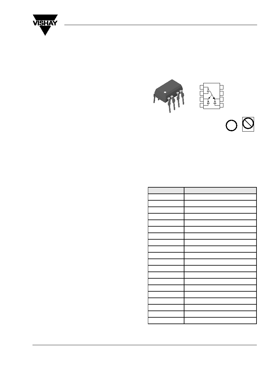
IL300
Document Number 83622
Rev. 1.4, 26-Oct-04
Vishay Semiconductors
www.vishay.com
1
i179026
A
C
NC
NC
C
A
A
C
1
2
3
4
8
7
6
5
K2
K1
Pb
Pb-free
e3
Linear Optocoupler, High Gain Stability, Wide Bandwidth
Features
∑ Couples AC and DC signals
∑ 0.01 % Servo Linearity
∑ Wide Bandwidth, > 200 kHz
∑ High Gain Stability, ± 0.05 %/ ∞C
∑ Low Input-Output Capacitance
∑ Low Power Consumption, < 15 mW
∑ Isolation Test Voltage, 5300 V
RMS
, 1.0 sec.
∑ Internal Insulation Distance, > 0.4 mm for VDE
∑ Lead-free component
∑ Component in accordance to RoHS 2002/95/EC
and WEEE 2002/96/EC
Agency Approvals
∑ UL File #E52744
∑ DIN EN 60747-5-2 (VDE0884)
DIN EN 60747-5-5 pending
Available with Option 1, Add -X001 Suffix
Applications
Power Supply Feedback Voltage/Current
Medical Sensor Isolation
Audio Signal Interfacing
Isolated Process Control Transducers
Digital Telephone Isolation
Description
The IL300 Linear Optocoupler consists of an AlGaAs
IRLED irradiating an isolated feedback and an output
PIN photodiode in a bifurcated arrangement. The
feedback photodiode captures a percentage of the
LED's flux and generates a control signal (I
P1
) that
can be used to servo the LED drive current. This tech-
nique compensates for the LED's non-linear, time,
and temperature characteristics. The output PIN pho-
todiode produces an output signal (I
P2
) that is linearly
related to the servo optical flux created by the LED.
The time and temperature stability of the input-output
coupler gain (K3) is insured by using matched PIN
photodiodes that accurately track the output flux of
the LED.
Order Information
For additional information on the available options refer to
Option Information.
Part
Remarks
IL300
K3 = 0.557 - 1.618, DIP-8
IL300-DEFG
K3 = 0.765 - 1.181, DIP-8
IL300-EF
K3 = 0.851 - 1.061, DIP-8
IL300-E
K3 = 0.851 - 0.955, DIP-8
IL300-F
K3 = 0.945 - 1.061, DIP-8
IL300-X006
K3 = 0.557 - 1.618, DIP-8 400mil (option 6)
IL300-X007
K3 = 0.557 - 1.618, SMD-8 (option 7)
IL300-X009
K3 = 0.557 - 1.618, SMD-8 (option 9)
IL300-DEFG-X006
K3 = 0.765 - 1.181, DIP-8 400 mil (option 6)
IL300-DEFG-X007
K3 = 0.765 - 1.181, SMD-8 (option 7)
IL300-DEFG-X009
K3 = 0.765 - 1.181, SMD-8 (option 9)
IL300-EF-X006
K3 = 0.851 - 1.061, DIP-8 400 mil (option 6)
IL300-EF-X007
K3 = 0.851 - 1.061, SMD-8 (option 7)
IL300-EF-X009
K3 = 0.851 - 1.061, SMD-8 (option 9)
IL300-E-X006
K3 = 0.851 - 0.955, DIP-8 400 mil (option 6)
IL300-E-X007
K3 = 0.851 - 0.955, SMD-8 (option 7)
IL300-E-X009
K3 = 0.851 - 0.955, SMD-8 (option 9)
IL300-F-X006
K3 = 0.945 - 1.061, DIP-8 400 mil (option 6)
IL300-F-X007
K3 = 0.945 - 1.061, SMD-8 (option 7)
IL300-F-X009
K3 = 0.945 - 1.061, SMD-8 (option 9)

www.vishay.com
2
Document Number 83622
Rev. 1.4, 26-Oct-04
VISHAY
IL300
Vishay Semiconductors
Operation Description
A typical application circuit (Figure 1) uses an opera-
tional amplifier at the circuit input to drive the LED.
The feedback photodiode sources current to R1 con-
nected to the inverting input of U1. The photocurrent,
I
P1
, will be of a magnitude to satisfy the relationship of
(I
P1
= V
IN
/R1).
The magnitude of this current is directly proportional
to the feedback transfer gain (K1) times the LED drive
current ( V
IN
/R1 = K1 ∑ I
F
). The op-amp will supply
LED current to force sufficient photocurrent to keep
the node voltage (Vb) equal to Va.
The output photodiode is connected to a non-invert-
ing voltage follower amplifier. The photodiode load
resistor, R2, performs the current to voltage conver-
sion. The output amplifier voltage is the product of the
output forward gain (K2) times the LED current and
photodiode load, R2 ( V
O
= I
F
∑ K2 ∑ R2).
Therefore, the overall transfer gain (V
O
/V
IN
) becomes
the ratio of the product of the output forward gain (K2)
times the photodiode load resistor (R2) to the product
of the feedback transfer gain (K1) times the input
resistor (R1). This reduces to
V
O
/V
IN
=(K2 ∑ R2)/(K1 ∑ R1).
The overall transfer gain is completely independent of
the LED forward current. The IL300 transfer gain (K3)
is expressed as the ratio of the output gain (K2) to the
feedback gain (K1). This shows that the circuit gain
becomes the product of the IL300 transfer gain times
the ratio of the output to input resistors
V
O
/V
IN
= K3 (R2/R1).
K1-Servo Gain
The ratio of the input photodiode current (I
P1
) to the
LED current (I
F
) i.e., K1 = I
P1
/I
F
.
K2-Forward Gain
The ratio of the output photodiode current (I
P2
) to the
LED current (I
F
), i.e., K2 = I
P2
/I
F
.
K3-Transfer Gain
The Transfer Gain is the ratio of the Forward Gain to
the Servo gain, i.e., K3 = K2/K1.
K3-Transfer Gain Linearity
The percent deviation of the Transfer Gain, as a func-
tion of LED or temperature from a specific Transfer
Gain at a fixed
LED current and temperature.
Photodiode
A silicon diode operating as a current source. The out-
put current is proportional to the incident optical flux
supplied by the LED emitter. The diode is operated in
the photovoltaic or photoconductive mode. In the pho-
tovoltaic mode the diode functions as a current
source in parallel with a forward biased silicon diode.
The magnitude of the output current and voltage is
dependent upon the load resistor and the incident
LED optical flux. When operated in the photoconduc-
tive mode the diode is connected to a bias supply
which reverse biases the silicon diode. The magni-
tude of the output current is directly proportional to the
LED incident optical flux.
LED (Light Emitting Diode)
An infrared emitter constructed of AlGaAs that emits
at 890 nm operates efficiently with drive current from
500
µA to 40 mA. Best linearity can be obtained at
drive currents between 5.0 mA to 20 mA. Its output
flux typically changes by - 0.5 % /∞C over the above
operational current range.
Application Circuit
Figure 1. Typical Application Circuit
iil300_01
8
7
6
5
K1
1
2
3
4
K2
R1
R2
IL300
Vb
Va
+
-
U1
Vin
lp 1
-
U2
+
lp 2
Vout
VCC
VCC
VCC
VCC
IF
Vc
+

VISHAY
IL300
Document Number 83622
Rev. 1.4, 26-Oct-04
Vishay Semiconductors
www.vishay.com
3
Absolute Maximum Ratings
T
amb
= 25 ∞C, unless otherwise specified
Stresses in excess of the absolute Maximum Ratings can cause permanent damage to the device. Functional operation of the device is
not implied at these or any other conditions in excess of those given in the operational sections of this document. Exposure to absolute
Maximum Rating for extended periods of the time can adversely affect reliability.
Input
Output
Coupler
Parameter
Test condition
Symbol
Value
Unit
Power dissipation
P
diss
160
mW
Derate linearly from 25 ∞C
2.13
mW/∞C
Forward current
I
F
60
mA
Surge current (pulse width < 10
µs)
I
PK
250
mA
Reverse voltage
V
R
5.0
V
Thermal resistance
R
th
470
K/W
Junction temperature
T
j
100
∞C
Parameter
Test condition
Symbol
Value
Unit
Power dissipation
P
diss
50
mA
Derate linearly from 25 ∞C
0.65
mW/∞C
Reverse voltage
V
R
50
V
Junction temperature
T
j
100
∞C
Thermal resistance
R
th
1500
K/W
Parameter
Test condition
Symbol
Value
Unit
Total package dissipation at
25 ∞C
P
tot
210
mW
Derate linearly from 25 ∞C
2.8
mW/∞C
Storage temperature
T
stg
- 55 to + 150
∞C
Operating temperature
T
amb
- 55 to + 100
∞C
Isolation test voltage
> 5300
V
RMS
Isolation resistance
V
IO
= 500 V, T
amb
= 25 ∞C
R
IO
> 10
12
V
IO
= 500 V, T
amb
= 100 ∞C
R
IO
> 10
11

www.vishay.com
4
Document Number 83622
Rev. 1.4, 26-Oct-04
VISHAY
IL300
Vishay Semiconductors
Electrical Characteristics
T
amb
= 25 ∞C, unless otherwise specified
Minimum and maximum values are testing requirements. Typical values are characteristics of the device and are the result of engineering
evaluation. Typical values are for information only and are not part of the testing requirements.
Input
LED Emitter
Output
Parameter
Test condition
Symbol
Min
Typ.
Max
Unit
Forward voltage
I
F
= 10 mA
V
F
1.25
1.50
V
V
F
Temperature coefficient
V
F
/
∞C
- 2.2
mV/∞C
Reverse current
V
R
= 5 V
I
R
1.0
µA
Junction capacitance
V
F
= 0 V, f = 1.0 MHz
C
j
15
pF
Dynamic resistance
I
F
= 10 mA
V
F
/
I
F
6.0
Parameter
Test condition
Symbol
Min
Typ.
Max
Unit
Dark current
V
det
= -15 V, I
F
= 0
µs
I
D
1.0
25
nA
Open circuit voltage
I
F
= 10 mA
V
D
500
mV
Short circuit current
I
F
= 10 mA
I
SC
70
µA
Junction capacitance
V
F
= 0, f = 1.0 MHz
C
j
12
pF
Noise equivalent power
V
det
= 15 V
NEP
4 x 10
14
W/
Hz

VISHAY
IL300
Document Number 83622
Rev. 1.4, 26-Oct-04
Vishay Semiconductors
www.vishay.com
5
Coupler
1. Bin Sorting:
K3 (transfer gain) is sorted into bins that are ± 6 % , as follows:
Bin A = 0.557 - 0.626
Bin B = 0.620 - 0.696
Bin C = 0.690 - 0.773
Bin D = 0.765 - 0.859
Bin E = 0.851 - 0.955
Bin F = 0.945 - 1.061
Bin G = 1.051 - 1.181
Bin H = 1.169 - 1.311
Bin I = 1.297 - 1.456
Bin J = 1.442 - 1.618
K3 = K2/K1. K3 is tested at I
F
= 10 mA, V
det
= - 15 V.
2. Bin Categories: All IL300s are sorted into a K3 bin, indicated by an alpha character that is marked on the part. The bins range from "A"
through "J".
The IL300 is shipped in tubes of 50 each. Each tube contains only one category of K3. The category of the parts in the tube is marked on
the tube label as well as on each individual part.
3. Category Options: Standard IL300 orders will be shipped from the categories that are available at the time of the order. Any of the ten
categories may be shipped. For customers requiring a narrower selection of bins, four different bin option parts are offered.
IL300-DEFG: Order this part number to receive categories D,E,F,G only.
IL300-EF: Order this part number to receive categories E, F only.
IL300-E: Order this part number to receive category E only.
Switching Characteristics
Parameter
Test condition
Symbol
Min
Typ.
Max
Unit
Input- output capacitance
V
F
= 0 V, f = 1.0 MHz
1.0
pF
K1, Servo gain (I
P1
/I
F
)
I
F
= 10 mA, V
det
= - 15 V
K1
0.0050
0.007
0.011
Servo current, see Note 1,2
I
F
= 10 mA, V
det
= - 15 V
I
P1
70
µA
K2, Forward gain (I
P2
/I
F
)
I
F
= 10 mA, V
det
= - 15 V
K2
0.0036
0.007
0.011
Forward current
I
F
= 10 mA, V
det
= - 15 V
I
P2
70
µA
K3, Transfer gain (K2/K1) see
Note 1,2
I
F
= 10 mA, V
det
= - 15 V
K3
0.56
1.00
1.65
K2/K1
Transfer gain linearity
I
F
= 1.0 to 10 mA
K3
± 0.25
%
I
F
= 1.0 to 10 mA,
T
amb
= 0 ∞C to 75 ∞C
± 0.5
%
Photoconductive Operation
Frequency response
I
Fq
= 10 mA, MOD = ± 4.0 mA,
R
L
= 50
BW (-3 db)
200
KHz
Phase response at 200 kHz
V
det
= - 15 V
-45
Deg.
Parameter
Test condition
Symbol
Min
Typ.
Max
Unit
Switching time
I
F
= 2.0 mA, I
Fq
= 10 mA
t
r
1.0
µs
t
f
1.0
µs
Rise time
t
r
1.75
µs
Fall time
t
f
1.75
µs