 | –≠–ª–µ–∫—Ç—Ä–æ–Ω–Ω—ã–π –∫–æ–º–ø–æ–Ω–µ–Ω—Ç: ILD251 | –°–∫–∞—á–∞—Ç—å:  PDF PDF  ZIP ZIP |
VISHAY
IL250/ 251/ 252/ ILD250/ 251/ 252
Document Number 83618
Rev. 1.3, 20-Apr-04
Vishay Semiconductors
www.vishay.com
1
i179024
1
2
3
6
5
4
B
C
E
NC
A/C
C/A
1
2
3
4
8
7
6
5
E
C
C
E
A
A
C
C
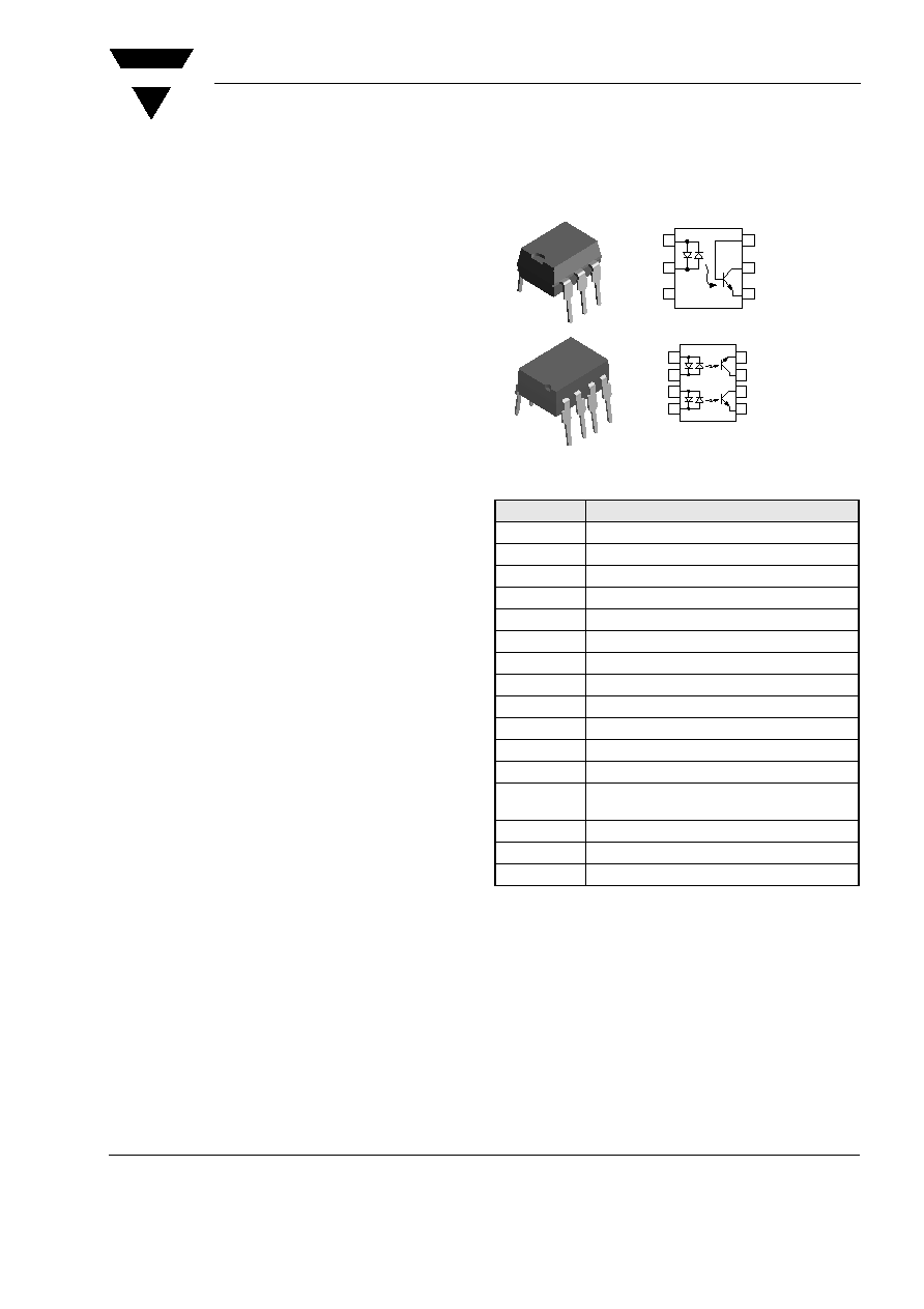
Single Channel
Dual Channel
Optocoupler, Phototransistor Output, AC Input, With Base
Connection
Features
∑ AC or Polarity Insensitive Input
∑ Built-in Reverse Polarity Input Protection
∑ Improved CTR Symmetry
∑ Industry Standard DIP Package
Agency Approvals
∑ UL File #E52744 System Code H or J
∑ CSA 93751
∑ BSI IEC60950 IEC60965
∑ DIN EN 60747-5-2(VDE0884)
DIN EN 60747-5-5 pending
Available with Option 1
Applications
Ideal for AC signal detection and monitoring.
Description
The IL250/ 251/ 252/ ILD250/ 251/ 252 are bidirec-
tional input optically coupled isolators consisting of
two Gallium Arsenide infrared LEDs coupled to a sili-
con NPN phototransistor per channel.
The IL250/ ILD/250 has a minimum CTR of 50 %,
the IL251/ ILD251 has a minimum CTR of 20 %,
and the IL252/ ILD252 has a minimum CTR of 100 %.
The IL250/ IL251/ IL252 are single channel optocou-
plers. The ILD250/ ILD251/ ILD252 has two isolated
channels in a single DIP package.
Order Information
For additional information on the available options refer to
Option Information.
Part
Remarks
IL250
CTR > 50 %, Single Channel DIP-6
IL251
CTR > 20 %, Single Channel DIP-6
IL252
CTR > 100 %, Single Channel DIP-6
ILD250
CTR > 50 %, Dual Channel DIP-8
ILD251
CTR > 20 %, Dual Channel DIP-8
ILD252
CTR > 100 %, Dual Channel DIP-8
IL250-X007
CTR > 50 %, Single Channel SMD-6 (option 7)
IL250-X009
CTR > 50 %, Single Channel SMD-6 (option 9)
IL251-X009
CTR > 20 %, Single Channel SMD-6 (option 9)
IL252-X007
CTR > 100 %, Single Channel SMD-6 (option 7)
IL252-X009
CTR > 100 %, Single Channel SMD-6 (option 9)
ILD250-X009
CTR > 50 %, Dual Channel SMD-6 (option 9)
ILD251-X006
CTR > 20 %, Dual Channel DIP-8 400 mil (option
6)
ILD251-X007
CTR > 20 %, Dual Channel SMD-6 (option 7)
ILD251-X009
CTR > 20 %, Dual Channel SMD-6 (option 9)
ILD252-X009
CTR > 100 %, Dual Channel SMD-6 (option 9)

www.vishay.com
2
Document Number 83618
Rev. 1.3, 20-Apr-04
VISHAY
IL250/ 251/ 252/ ILD250/ 251/ 252
Vishay Semiconductors
Absolute Maximum Ratings
T
amb
= 25 ∞C, unless otherwise specified
Stresses in excess of the absolute Maximum Ratings can cause permanent damage to the device. Functional operation of the device is
not implied at these or any other conditions in excess of those given in the operational sections of this document. Exposure to absolute
Maximum Rating for extended periods of the time can adversely affect reliability.
Input
Output
Coupler
Parameter
Test condition
Symbol
Value
Unit
Forward continuous current
I
F
60
mA
Power dissipation
P
diss
100
mW
Derate linearly from 25 ∞C
1.33
mw/∞C
Parameter
Test condition
Symbol
Value
Unit
Collector-emitter breakdown voltage
BV
CEO
30
V
Emitter-base breakdown voltage
BV
EBO
5.0
V
Collector-base breakdown voltage
BV
CBO
70
V
Power dissipation single channel
P
diss
200
mW
Power dissipation dual channel
P
diss
150
mW
Derate linearly from 25 ∞C single channel
2.6
mW/∞C
Derate linearly from 25 ∞C dual channel
2.0
mW/∞C
Parameter
Test condition
Symbol
Value
Unit
Isolation test voltage (between
emitter and detector referred to
standard climate
23 ∞C/50 %RH, DIN 50014)
V
ISO
5300
V
RMS
Creepage
7.0
mm
Clearance
7.0
mm
Isolation resistance
V
IO
= 500 V, T
amb
= 25 ∞C
R
IO
10
12
V
IO
= 500 V, T
amb
= 100 ∞C
R
IO
10
11
Total dissipation single channel
P
tot
250
mW
Total dissipation dual channel
P
tot
400
mW
Derate linearly from 25 ∞C single
channel
3.3
mW/∞C
Derate linearly from 25 ∞C dual
channel
5.3
mW/∞C
Storage temperature
T
stg
- 55 to + 150
∞C
Operating temperature
T
amb
- 55 to + 100
∞C
Lead soldering time at 260 ∞C
10
sec.

VISHAY
IL250/ 251/ 252/ ILD250/ 251/ 252
Document Number 83618
Rev. 1.3, 20-Apr-04
Vishay Semiconductors
www.vishay.com
3
Electrical Characteristics
T
amb
= 25 ∞C, unless otherwise specified
Minimum and maximum values are testing requirements. Typical values are characteristics of the device and are the result of engineering
evaluation. Typical values are for information only and are not part of the testing requirements.
Input
Output
Coupler
Current Transfer Ratio
Typical Characteristics
(T
amb
= 25
∞C unless otherwise specified)
Parameter
Test condition
Symbol
Min
Typ.
Max
Unit
Forward voltage
I
F
= ± 10 mA
V
F
1.2
1.5
V
Parameter
Test condition
Symbol
Min
Typ.
Max
Unit
Collector-emitter breakdown voltage
I
C
= 1.0 mA
BV
CEO
30
50
V
Emitter-base breakdown voltage
I
E
= 100
µA
BV
EBO
7.0
10
V
Collector-base breakdown voltage
I
C
= 10
µA
BV
CBO
70
90
V
Collector-emitter leakage current
V
CE
= 10 V
I
CEO
5.0
50
nA
Parameter
Test condition
Symbol
Min
Typ.
Max
Unit
Collector-emitter saturation
voltage
I
F
= ± 16 mA, I
C
= 2.0 mA
V
CEsat
0.4
V
Parameter
Test condition
Part
Symbol
Min
Typ.
Max
Unit
DC Current Transfer Ratio
I
F
= ± 10 mA, V
CE
= 10 V
ILD250
CTR
DC
50
%
ILD251
CTR
DC
20
%
ILD252
CTR
DC
100
%
Symmetry (CTR @ + 10 mA)/
(CTR @ -10 mA)
0.50
1.0
2.0
Fig. 1 LED Forward Current vs.Forward Voltage
iil250_01
-1.5
-1.0
-0.5
0.0
0.5
1.0
1.5
-60
-40
-20
0
20
40
60
25∞C
-55∞C
85∞C
VF - LED Forward Voltage - V
I F
-
LED
Forward
Current
-
m
A
Fig. 2 Normalized Non-Saturated and Saturated CTR vs. LED
Current
iil250_02
100
10
1
.1
0.0
0.5
1.0
1.5
NCTR(SAT)
NCTR
IF - LED Current - mA
NCTR
-
Normalized
CTR
Normalized to:
VCE = 10 V, IF = 10 mA
TA= 25∞C
CTRce(sat) VCE = 0.4 V

www.vishay.com
4
Document Number 83618
Rev. 1.3, 20-Apr-04
VISHAY
IL250/ 251/ 252/ ILD250/ 251/ 252
Vishay Semiconductors
Fig. 3 Normalized Non-saturated and Saturated CTR vs. LED
Current
Fig. 4 Normalized Non-saturated and saturated CTR vs. LED
Current
Fig. 5 Normalized Non-saturated and saturated CTR vs. LED
Current
iil250_03
100
10
1
.1
0.0
0.5
1.0
1.5
NCTR(SAT)
NCTR
IF - LED Current - mA
NCTR
-
Normalized
CTR
Normalized to:
VCE = 10 V, IF = 10 mA, TA= 25∞C
TA= 50∞C
CTRce(sat) VCE = 0.4 V
iil250_04
100
10
1
.1
0.0
0.5
1.0
1.5
IF - LED Current - mA
NCTR(SAT)
NCTR
Normalized to:
VCE = 10 V, IF = 10 mA
TA= 25∞C
CTRce(sat) VCE = 0.4 V
TA= 70∞C
NCTR
-
Normalized
CTR
iil250_05
.1
1
10
100
1.5
1.0
0.5
0.0
IF - LED Current - mA
NCTR
-
Normalized
CTR
NCTR(SAT)
NCTR
Normalized to:
VCE = 10 V, IF = 10 mA, TA = 25∞C
CTRce(sat) VCE = 0.4 V
TA = 85∞C
Fig. 6 Collector-Emitter Current vs. Temperature and LED
Current
Fig. 7 Collector-Emitter Leakage Current vs.Temp.
Fig. 8 Normalized CTR
cb
vs. LED Current and Temperature
iil250_06
60
50
30
20
10
0
0
5
10
15
20
25
30
35
50∞C
70∞C
85∞C
IF - LED Current - mA
I CE
-
C
ollector
Current
-
m
A
25∞C
40
iil250_07
100
80
60
40
20
0
-20
TA - Ambient Temperature - ∞C
I CEO
-
Collector-Emitter
-
n
A
TYPICAL
VCE = 10 V
10 5
10 4
10 3
10 2
10 1
10 0
10 -1
10 -2
iil250_08
.1
1
1 0
100
0.0
0.5
1.0
1.5
25∞C
50∞C
70∞C
IF - LED Current - mA
NCTR
cb
-
Normalized
CTR
cb
Normalized to:
IF =10 mA
VCB = 9.3 V
TA = 25∞C

VISHAY
IL250/ 251/ 252/ ILD250/ 251/ 252
Document Number 83618
Rev. 1.3, 20-Apr-04
Vishay Semiconductors
www.vishay.com
5
Fig. 9 Collector-Base Photocurrent vs. LED Current
Fig. 10 Normalized Photocurrent vs. I
F
and Temp.
Fig. 11 Normalized Non-saturated HFE vs. Base Current and
Temperature
iil250_09
100
10
1
.1
.01
.1
1
10
100
1000
IF - LED Current - mA
I CB
-
Collector
Base
Photocurrent
-
µ
A
ICB = 1.0357 *IF ^1.3631
TA = 25∞C
iil250_10
.1
1
10
100
10
1
.1
.01
I
F
- LED Current - mA
Normalized
Photocurrent
Normalized to:
IF = 10 mA, T = 25∞C
NIB-TA = -20∞C
NIb, TA = 25∞C
NIb, TA = 50∞C
NIb, TA = 70∞C
iil250_11
1000
0.4
0.6
0.8
1.0
1.2
IB - Base Current - µA
NHFE
-
Normalized
HFE
-20∞C
25∞C
50∞C
70∞C
Normalized to:
IB= 20 µA
VCE = 10 V
TA = 25∞C
1
10
100
Fig. 12 Normalized Saturated HFE vs. Base Current and
Temperature
Fig. 13 Propagation Delay vs. Collector Load Resistor
Fig. 14 Switching Timing
iil250_12
1
1 0
100
1000
0.0
0.5
1.0
1.5
IB - Base Current - (µA)
V CE = 0.4 V
Normalized to:
VCE = 10 V
IB = 20 µA
TA = 25∞C
70∞C
50∞C
25∞C
-20∞C
NHFE(sat)
-Normalized
Saturated
HFE
iil250_13
RL - Collector Load Resistor - k
100
10
1
.1
1
10
100
1000
1.0
1.5
2.0
2.5
tpLH
tpHL
tpLH
-
P
ropagation
D
elay
µ
s
tpHL
-
P
ropagation
Delay
µ
s
TA = 25∞C, IF = 10 mA
VCC = 5 V, Vth = 1.5 V
iil250_14
IF
tR
VO
tD
tS
tF
tPHL
tPLH
VTH = 1.5 V