 | –≠–ª–µ–∫—Ç—Ä–æ–Ω–Ω—ã–π –∫–æ–º–ø–æ–Ω–µ–Ω—Ç: ILD610-1 | –°–∫–∞—á–∞—Ç—å:  PDF PDF  ZIP ZIP |

VISHAY
ILD610
Document Number 83651
Rev. 1.6, 26-Oct-04
Vishay Semiconductors
www.vishay.com
1
i179045
8
7
6
5
E
C
E
C
A
C
A
C
1
2
3
4
Pb
Pb-free
e3
Optocoupler, Phototransistor Output, Dual Channel
Features
∑ Dual Version of SFH610 Series
∑ Isolation Test Voltage, 5300 V
RMS
∑ V
CEsat
0.25 (
0.4) V at I
F
= 10 mA, I
C
= 2.5 mA
∑ V
CEO
= 70 V
∑ Lead-free component
∑ Component in accordance to RoHS 2002/95/EC
and WEEE 2002/96/EC
Agency Approvals
∑ UL1577, File No. E52744 System Code H or J,
Double Protection
∑ DIN EN 60747-5-2 (VDE0884)
DIN EN 60747-5-5 pending
Available with Option 1
∑ CSA 93751
∑ BSI IEC60950 IEC60065
Description
The ILD610 series is a dual channel optocoupler
series for high density applications. Each channel
consists of an optically coupled pair with a Gallium
Arsenide infrared LED and silicon NPN phototransis-
tor. Signal information, including a DC level, can be
transmitted by the device while maintaining a high
degree of electrical isolation between input and out-
put. The ILD610 series is the dual version of SFH610
series and uses a repetitive pin-out configuration
instead of the more common alternating pin-out used
in most dual couplers.
Order Information
For additional information on the available options refer to
Option Information.
Absolute Maximum Ratings
T
amb
= 25 ∞C, unless otherwise specified
Stresses in excess of the absolute Maximum Ratings can cause permanent damage to the device. Functional operation of the device is
not implied at these or any other conditions in excess of those given in the operational sections of this document. Exposure to absolute
Maximum Rating for extended periods of the time can adversely affect reliability.
Input
Part
Remarks
ILD610-1
CTR 40 - 80 %, DIP-8
ILD610-2
CTR 63 - 125 %, DIP-8
ILD610-3
CTR 100 - 200 %, DIP-8
ILD610-4
CTR 160 - 320 %, DIP-8
ILD610-2X007
CTR 63 - 125 %, SMD-8 (option 7)
ILD610-3X006
CTR 100 - 200 %, DIP-8 400 mil (option 6)
ILD610-3X009
CTR 100 - 200 %, SMD-8 (option 9)
ILD610-4X009
CTR 160 - 320 %, SMD-8 (option 9)
Parameter
Test condition
Symbol
Value
Unit
Reverse voltage
V
R
6.0
V
Surge forward current
t
10 ms
I
FSM
1.5
A
Power dissipation
P
diss
100
mW
Derate linearly from 25 ∞C
1.3
mW/∞C
DC forward current
I
F
60
mA

www.vishay.com
2
Document Number 83651
Rev. 1.6, 26-Oct-04
VISHAY
ILD610
Vishay Semiconductors
Output
Coupler
Electrical Characteristics
T
amb
= 25 ∞C, unless otherwise specified
Minimum and maximum values are testing requirements. Typical values are characteristics of the device and are the result of engineering
evaluation. Typical values are for information only and are not part of the testing requirements.
Input
Output
Coupler
Parameter
Test condition
Symbol
Value
Unit
Collector-emitter voltage
V
CE
70
V
Collector current
I
C
50
mA
t
1.0 ms
I
C
100
mA
Power dissipation
P
diss
150
mW
Derate linearly from 25 ∞C
2.0
mW/∞C
Parameter
Test condition
Symbol
Value
Unit
Isolation test voltage
t = 1.0 sec.
V
ISO
5300
V
RMS
Isolation resistance
V
IO
= 500 V, T
amb
= 25 ∞C
R
IO
10
12
V
IO
= 500 V,T
amb
= 100 ∞C
R
IO
10
11
Storage temperature
T
stg
- 55 to + 150
∞C
Operating temperature
T
amb
- 55 to + 100
∞C
Junction temperature
T
j
100
∞C
Lead soldering time at 260 ∞C
10
sec.
Parameter
Test condition
Symbol
Min
Typ.
Max
Unit
Forward voltage
I
F
= 60 mA
V
F
1.25
1.65
V
Reverse current
V
R
= 6.0 V
I
R
0.01
10
µA
Capacitance
V
R
= 0 V, f = 1.0 MHz
C
O
25
pF
Parameter
Test condition
Part
Symbol
Min
Typ.
Max
Unit
Collector-emitter breakdown
voltage
I
C
= 10 mA, I
E
= 10
µA
BV
CEO
70
90
V
BV
CEO
6.0
7.0
V
Collector-emitter dark current
V
CE
= 10 V
I
CEO
2.0
50
nA
Collector-emitter capacitance
V
CE
= 5.0 V, f = 1.0 MHz
C
CE
7.0
pF
Collector-emitter leakage
current
V
CE
= 10 V
ILD610-1
I
CEO
2.0
50
nA
ILD610-2
I
CEO
2.0
50
nA
ILD610-3
I
CEO
5.0
100
nA
ILD610-4
I
CEO
5.0
100
nA
Parameter
Test condition
Symbol
Min
Typ.
Max
Unit
Collector-emitter saturation
voltage
I
F
= 10 mA, I
C
= 2.5 mA
V
CEsat
0.25
0.40
V
Coupling capacitance
C
C
0.35
pF

VISHAY
ILD610
Document Number 83651
Rev. 1.6, 26-Oct-04
Vishay Semiconductors
www.vishay.com
3
Current Transfer Ratio
1)
CTR will match within a ratio of 1.7:1
Switching Characteristics
Non-saturated
Saturated
Parameter
Test condition
Part
Symbol
Min
Typ.
Max
Unit
CTR
1)
I
F
= 10 mA, V
CE
= 5.0 V
ILD610-1
CTR
40
80
%
ILD610-2
CTR
63
125
%
ILD610-3
CTR
100
200
%
ILD610-4
CTR
160
320
%
I
F
= 1.0 mA, V
CE
= 5.0 V
ILD610-1
CTR
13
%
ILD610-2
CTR
22
%
ILD610-3
CTR
34
%
ILD610-4
CTR
56
%
Parameter
Test condition
Part
Symbol
Min
Typ.
Max
Unit
Rise time
V
CC
= 5.0, R
L
= 75
, I
F
= 10 mA
ILD610-1
t
r
2.0
µ
ILD610-2
t
r
2.5
µ
ILD610-3
t
r
2.9
µ
ILD610-4
t
r
3.3
µ
Fall time
V
CC
= 5.0, R
L
= 75
, I
F
= 10 mA
ILD610-1
t
f
2.0
µ
ILD610-2
t
f
2.6
µ
ILD610-3
t
f
3.1
µ
ILD610-4
t
f
3.5
µ
Turn-on time
V
CC
= 5.0, R
L
= 75
, I
F
= 10 mA
ILD610-1
t
on
3.0
µ
ILD610-2
t
on
3.2
µ
ILD610-3
t
on
3.6
µ
ILD610-4
t
on
2.3
µ
Turn-off time
V
CC
= 5.0, R
L
= 75
, I
F
= 10 mA
ILD610-1
t
off
2.9
µ
ILD610-2
t
off
3.4
µ
ILD610-3
t
off
3.7
µ
ILD610-4
t
off
4.1
µ
Parameter
Test condition
Part
Symbol
Min
Typ.
Max
Unit
Rise time
V
CC
= 5.0, R
L
= 1.0 k
, I
F
= 5.0 mA
ILD610-1
t
r
2.0
µ
ILD610-2
t
r
2.8
µ
ILD610-3
t
r
3.3
µ
ILD610-4
t
r
4.6
µ
Fall time
V
CC
= 5.0, R
L
= 1.0 k
, I
F
= 5.0 mA
ILD610-1
t
f
11
µ
ILD610-2
t
f
2.6
µ
ILD610-3
t
f
3.1
µ
ILD610-4
t
f
15
µ
Turn-on time
V
CC
= 5.0, R
L
= 1.0 k
, I
F
= 5.0 mA
ILD610-1
t
on
3.0
µ
ILD610-2
t
on
4.3
µ
ILD610-3
t
on
4.6
µ
ILD610-4
t
on
6.0
µ

www.vishay.com
4
Document Number 83651
Rev. 1.6, 26-Oct-04
VISHAY
ILD610
Vishay Semiconductors
Typical Characteristics (Tamb = 25
∞C unless otherwise specified)
Turn-off time
V
CC
= 5.0, R
L
= 1.0 k
, I
F
= 5.0 mA
ILD610-1
t
off
18
µ
ILD610-2
t
off
2.9
µ
ILD610-3
t
off
3.4
µ
ILD610-4
t
off
25
µ
Parameter
Test condition
Part
Symbol
Min
Typ.
Max
Unit
Figure 1. Forward Voltage vs. Forward Current
Figure 2. Normalized Non-Saturated and Saturated CTR vs. LED
Current
iilct6_01
IF - Forward Current - mA
100
10
1
.1
0.7
0.8
0.9
1.0
1.1
1.2
1. 3
1.4
VF
-
F
orward
Voltage
-
V
Ta = ≠55∞C
Ta = 25∞C
Ta = 85∞C
iilct6_02
100
10
1
.1
0.0
0.5
1.0
1.5
NCTR(SAT)
NCTR
IF - LED Current - mA
NCTR
-
Normalized
CTR
Normalized to:
VCE = 10 V, IF = 10 mA
TA= 25∞C
CTRce(sat) VCE = 0.4 V
Figure 3. Normalized Non-Saturated and Saturated CTR vs. LED
Current
Figure 4. Normalized Non-Saturated and Saturated CTR vs. LED
Current
iilct6_03
100
10
1
.1
0.0
0.5
1.0
1.5
NCTR(SAT)
NCTR
IF - LED Current - mA
NCTR
-
Normalized
CTR
Normalized to:
VCE = 10 V, IF = 10 mA, TA= 25∞C
TA= 50∞C
CTRce(sat) VCE = 0.4 V
iilct6_04
100
10
1
.1
0.0
0.5
1.0
1.5
IF - LED Current - mA
NCTR(SAT)
NCTR
Normalized to:
VCE = 10 V, IF = 10 mA
TA= 25∞C
CTRce(sat) VCE = 0.4 V
TA= 70∞C
NCTR
-
Normalized
CTR
VISHAY
ILD610
Document Number 83651
Rev. 1.6, 26-Oct-04
Vishay Semiconductors
www.vishay.com
5
Figure 5. Normalized Non-Saturated and Saturated CTR vs. LED
Current
Figure 6. Collector-Emitter Current vs. Temperature and LED
Current
Figure 7. Collector-Emitter Leakage Current vs.Temp.
iilct6_05
.1
1
10
100
1.5
1.0
0.5
0.0
IF - LED Current - mA
NCTR
-
Normalized
CTR
NCTR(SAT)
NCTR
Normalized to:
VCE = 10 V, IF = 10 mA, TA = 25∞C
CTRce(sat) VCE = 0.4 V
TA = 85∞C
iilct6_06
60
50
30
20
10
0
0
5
10
15
20
25
30
35
50∞C
70∞C
85∞C
IF - LED Current - mA
I CE
-
C
ollector
Current
-
m
A
25∞C
40
iilct6_07
100
80
60
40
20
0
-20
10
10
10
10
10
10
10
10
-2
-1
0
1
2
3
4
5
TA - Ambient Temperature - ∞C
I CEO
-
Collector-Emitter
-
n
A
Vce = 10 V
Typical
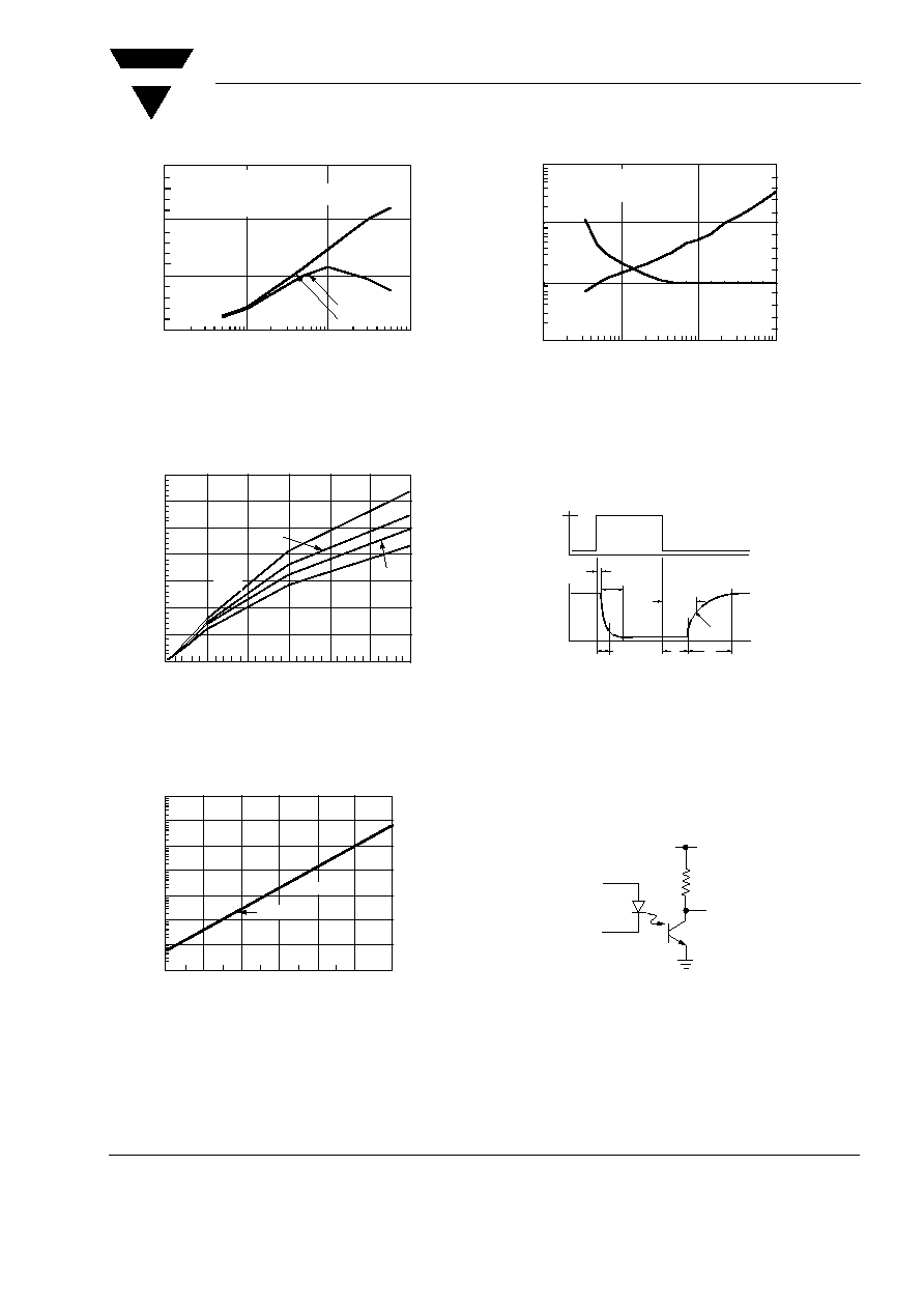
Figure 8. Propagation Delay vs. Collector Load Resistor
Figure 9. Switching Timing
Figure 10. Non-saturated Switching Schematic
iilct6_08
RL - Collector Load Resistor - k
100
10
1
.1
1
10
100
1000
1.0
1.5
2.0
2.5
tpLH
tpHL
t pLH
-
P
ropagation
D
elay
µ
s
t pHL
-
Propagation
Delay
µ
s
Ta = 25∞C, IF = 10 mA
Vcc = 5 V, Vth = 1.5 V
iild610_09
IF
tR
VO
tD
tS
tF
tPHL
tPLH
VTH=1.5 V
iild610_10
VO
VCC=5 V
R L
F=10 KHz
DF=50%
IF =10 mA