 | –≠–ª–µ–∫—Ç—Ä–æ–Ω–Ω—ã–π –∫–æ–º–ø–æ–Ω–µ–Ω—Ç: ILD620 | –°–∫–∞—á–∞—Ç—å:  PDF PDF  ZIP ZIP |

VISHAY
ILD620/ 620GB / ILQ620/ 620GB
Document Number 83653
Rev. 1.3, 26-Apr-04
Vishay Semiconductors
www.vishay.com
1
E
C
C
E
E
C
C
E
16
15
14
13
12
11
10
9
1
2
3
4
5
6
7
8
i179053
E
C
C
E
1
2
3
4
8
7
6
5
A/C
A/C
A/C
A/C
A/C
A/C
A/C
A/C
A/C
A/C
A/C
A/C
Dual Channel
Quad Channel
Optocoupler, Phototransistor Output, AC Input (Dual, Quad
Channel)
Features
∑ Identical Channel to Channel Footprint
∑ ILD620 Crosses to TLP620-2
∑ ILQ620 Crosses to TLP620-4
∑ High Collector-Emitter Voltage, BV
CEO
= 70 V
∑ Dual and Quad Packages Feature:
- Reduced Board Space
- Lower Pin and Parts Count
- Better Channel to Channel CTR Match
- Improved Common Mode Rejection
∑ Isolation Test Voltage 5300 V
RMS
Agency Approvals
∑ UL File #E52744 System Code H or J
∑ CSA 93751
∑ DIN EN 60747-5-2(VDE0884)
DIN EN 60747-5-5 pending
Available with Option 1
∑ BSI IEC60950 IEC60965
Description
The ILD620/ ILQ620 and ILD620GB/ ILQ620GB are
multi-channel input phototransistor optocouplers that
use inverse parallel GaAs IRLED emitter and high
gain NPN silicon phototransistors per channel. These
devices are constructed using over/under leadframe
optical coupling and double molded insulation result-
ing in a withstand test voltage of 5300 V
RMS
.
The LED parameters and the linear CTR characteris-
tics make these devices well suited for AC voltage
detection. the ILD/Q620GB with its low I
F
quaranteed
CTR
CEsat
minimizes power dissipation of the AC volt-
age detection network that is placed in series with the
LEDs. Eliminating the phototransistor base connec-
tion provides added electrical noise immunity from the
transients found in many industrial control environ-
ments.
Order Information
For additional information on the available options refer to
Option Information.
Part
Remarks
ILD620
CTR > 50 %, DIP-8
ILD620GB
CTR > 100 %, DIP-8
ILQ620
CTR > 50 %, DIP-16
ILQ620GB
CTR > 100 %, DIP-16
ILD620-X007
CTR > 50 %, SMD-8 (option 7)
ILD620-X009
CTR > 50 %, SMD-8 (option 9)
ILD620GB-X009
CTR > 100 %, SMD-8 (option 9)
ILQ620-X009
CTR > 50 %, SMD-16 (option 9)
ILQ620GB-X009
CTR > 100 %, SMD-16 (option 9)
www.vishay.com
2
Document Number 83653
Rev. 1.3, 26-Apr-04
VISHAY
ILD620/ 620GB / ILQ620/ 620GB
Vishay Semiconductors
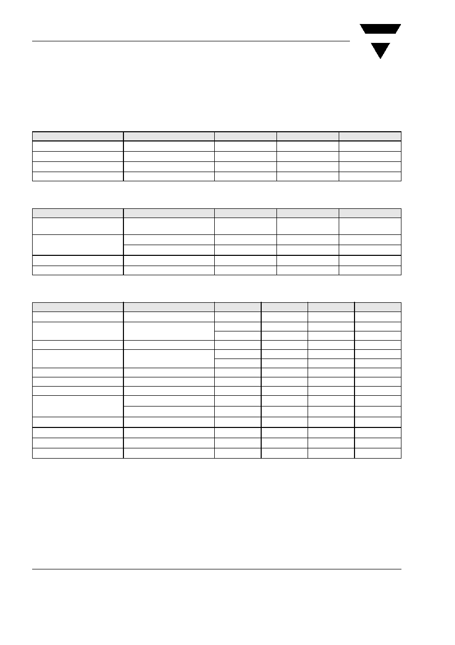
Absolute Maximum Ratings
T
amb
= 25 ∞C, unless otherwise specified
Stresses in excess of the absolute Maximum Ratings can cause permanent damage to the device. Functional operation of the device is
not implied at these or any other conditions in excess of those given in the operational sections of this document. Exposure to absolute
Maximum Rating for extended periods of the time can adversely affect reliability.
Input
Output
Coupler
Parameter
Test condition
Symbol
Value
Unit
Forward current
I
F
± 60
mA
Surge current
I
FSM
± 1.5
A
Power dissipation
P
diss
100
mW
Derate linearly from 25 ∞C
1.3
mW/∞C
Parameter
Test condition
Symbol
Value
Unit
Collector-emitter breakdown
voltage
BV
CEO
70
V
Collector current
I
C
50
mA
t < 1.0 sec:
I
C
100
mA
Power dissipation
P
diss
150
mW
Derate from 25 ∞C
2.0
mW/∞C
Parameter
Test condition
Part
Symbol
Value
Unit
Isolation test voltage
t = 1.0 sec.
V
ISO
5300
V
RMS
Package dissipation
ILD620
400
mW
ILD620GB
400
mW
Derate from 25 ∞C
5.33
mW/∞C
Package dissipation
ILQ620
500
mW
ILQ620GB
500
mW
Derate from 25 ∞C
6.67
mW/∞C
Creepage
7.0
mm
Clearance
7.0
mm
Isolation resistance
V
IO
= 500 V, T
amb
= 25 ∞C
R
IO
10
12
V
IO
= 500 V, T
amb
= 100 ∞C
R
IO
10
11
Storage temperature
T
stg
- 55 to + 150
∞C
Operating temperature
T
amb
- 55 to + 100
∞C
Junction temperature
T
j
100
∞C
Soldering temperature
2.0 mm from case bottom
T
sld
260
∞C

VISHAY
ILD620/ 620GB / ILQ620/ 620GB
Document Number 83653
Rev. 1.3, 26-Apr-04
Vishay Semiconductors
www.vishay.com
3
Electrical Characteristics
T
amb
= 25 ∞C, unless otherwise specified
Minimum and maximum values are testing requirements. Typical values are characteristics of the device and are the result of engineering
evaluation. Typical values are for information only and are not part of the testing requirements.
Input
Output
Coupler
Current Transfer Ratio
Parameter
Test condition
Symbol
Min
Typ.
Max
Unit
Forward voltage
I
F
= ± 10 mA
V
F
1.0
1.15
1.3
V
Forward current
V
R
= ± 0.7 V
I
F
2.5
20
µA
Capacitance
V
F
= 0 V, f = 1.0 MHz
C
O
25
pF
Thermal resistance, junction to
lead
R
THJL
750
K/W
Parameter
Test condition
Symbol
Min
Typ.
Max
Unit
Collector-emitter capacitance
V
CE
= 5.0 V, f = 1.0 MHz
C
CE
6.8
pF
Collector-emitter leakage
current
V
CE
= 24 V
I
CEO
10
100
nA
T
A
= 85 ∞C, V
CE
= 24 V
I
CEO
2.0
50
µA
Thermal resistance, junction to
lead
R
THJL
500
K/W
Parameter
Test condition
Part
Symbol
Min
Typ.
Max
Unit
Off-state collector current
V
F
= ± 0.7 V, V
CE
= 24 V
I
CE(OFF)
1.0
10
µA
Collector-emitter saturation
voltage
I
F
= ± 8.0 mA, I
CE
= 2.4 mA
ILD620
V
CEsat
0.4
V
ILQ620
V
CEsat
0.4
V
I
F
= ± 1.0 mA, I
CE
= 0.2 mA
ILD620GB
V
CEsat
0.4
V
ILQ620GB
V
CEsat
0.4
V
Parameter
Test condition
Part
Symbol
Min
Typ.
Max
Unit
Channel/Channel CTR match
I
F
= ± 5.0 mA, V
CE
= 5.0 V
CTRX/CTRY
1 to 1
3 to 1
CTR symmetry
I
CE
(I
F
= - 5.0 mA)/
I
CE
(I
F
= + 5.0 mA)
I
CE(RATIO)
0.5
2.0
Current Transfer Ratio
(collector-emitter saturated)
I
F
= ± 1.0 mA, V
CE
= 0.4 V
ILD620
CTR
CEsat
60
%
ILQ620
CTR
CEsat
60
%
Current Transfer Ratio
(collector-emitter)
I
F
= ± 5.0 mA, V
CE
= 5.0 V
ILD620
CTR
CE
50
80
600
%
ILQ620
CTR
CE
50
80
600
%
Current Transfer Ratio
(collector-emitter saturated)
I
F
= ± 1.0 mA, V
CE
= 0.4 V
ILD620GB
CTR
CEsat
30
%
ILQ620GB
CTR
CEsat
30
%
Current Transfer Ratio
(collector-emitter)
I
F
= ± 5.0 mA, V
CE
= 5.0 V
ILD620GB
CTR
CE
100
200
600
%
ILQ620GB
CTR
CE
100
200
600
%

www.vishay.com
4
Document Number 83653
Rev. 1.3, 26-Apr-04
VISHAY
ILD620/ 620GB / ILQ620/ 620GB
Vishay Semiconductors
Switching Characteristics
Non-saturated
Saturated
Typical Characteristics
(T
amb
= 25
∞C unless otherwise specified)
Parameter
Test condition
Symbol
Min
Typ.
Max
Unit
On time
I
F
= ± 10 mA, V
CC
= 5.0 V,
R
L
= 75
, 50 % of V
PP
t
on
3.0
µs
Rise time
I
F
= ± 10 mA, V
CC
= 5.0 V,
R
L
= 75
, 50 % of V
PP
t
r
20
µs
Off time
I
F
= ± 10 mA, V
CC
= 5.0 V,
R
L
= 75
, 50 % of V
PP
t
off
2.3
µs
Fall time
I
F
= ± 10 mA, V
CC
= 5.0 V,
R
L
= 75
, 50 % of V
PP
t
f
2.0
µs
Propagation H-L
I
F
= ± 10 mA, V
CC
= 5.0 V,
R
L
= 75
, 50 % of V
PP
t
PHL
1.1
µs
Propagation L-H
I
F
= ± 10 mA, V
CC
= 5.0 V,
R
L
= 75
, 50 % of V
PP
t
PLH
2.5
µs
Parameter
Test condition
Symbol
Min
Typ.
Max
Unit
On time
I
F
= ± 10 mA, V
CC
= 5.0 V,
R
L
= 1.0 K
, V
TH
= 1.5 V
t
on
4.3
µs
Rise time
I
F
= ± 10 mA, V
CC
= 5.0 V,
R
L
= 1.0 K
, V
TH
= 1.5 V
t
r
2.8
µs
Off time
I
F
= ± 10 mA, V
CC
= 5.0 V,
R
L
= 1.0 K
, V
TH
= 1.5 V
t
off
2.5
µs
Fall time
I
F
= ± 10 mA, V
CC
= 5.0 V,
R
L
= 1.0 K
, V
TH
= 1.5 V
t
f
11
µs
Propagation H-L
I
F
= ± 10 mA, V
CC
= 5.0 V,
R
L
= 1.0 K
, V
TH
= 1.5 V
t
PHL
2.6
µs
Propagation L-H
I
F
= ± 10 mA, V
CC
= 5.0 V,
R
L
= 1.0 K
, V
TH
= 1.5 V
t
PLH
7.2
µs
Fig. 1 Non-saturated Switching Timing
iild620_01
VO
VCC = 5 V
RL = 75
F = 10 KHz,
DF = 50%
IF = 10 mA
Fig. 2 Saturated Switching Timing
iild620_02
VO
VCC = 5 V
RL = 1 k
F = 10 KHz,
DF = 50%
IF = 10 mA

VISHAY
ILD620/ 620GB / ILQ620/ 620GB
Document Number 83653
Rev. 1.3, 26-Apr-04
Vishay Semiconductors
www.vishay.com
5
Fig. 3 Non-saturated Switching Timing
Fig. 4 Saturated Switching Timing
Fig. 5 LED Forward Current vs.Forward Voltage
iild620_03
t
R
t
F
t
D
50%
t
PLH
V
O
I
F
t
PLH
t
S
t
on
t
off
iild620 _04
IF
t
R
V
O
t
D
t
S
t
F
t
PHL
t
PLH
V
TH
= 1.5 V
iild620_05
-1.5
-1.0
-0.5
0.0
0.5
1.0
1.5
60
40
20
0
-20
-40
-60
≠55 ∞C
VF - LED Forward Voltage - V
I F
-
L
ED
Forward
Current
-
m
A
85 ∞C
25 ∞C
Fig. 6 Collector-Emitter Leakage vs. Temperature
Fig. 7 Maximum LED Current vs. Ambient Temperature
Fig. 8 Maximum LED Power Dissipation
iild620_06
100
80
60
40
20
0
-20
10
10
10
10
10
10
10
10
-2
-1
0
1
2
3
4
5
TA - Ambient Temperature - ∞C
I CEO
-
Collector-Emitter
-
n
A
Vce = 10 V
Typical
-60
-40
-20
0
20
40
60
80
100
120
100
80
60
40
0
20
Ta - Ambient Temperature - ∞C
IF
-
M
aximum
LED
Current
-
m
A
TJ (MAX) = 100 ∞C
iild620_07
iild620_08
-60 -40
-20
0
20
40
60
80
100
200
100
0
50
Ta - Ambient Temperature - ∞C
P
LED
-
LED
Power
-
m
W
150