
VISHAY
ILD621/ GB/ ILQ621/ GB
Document Number 83654
Rev. 1.3, 19-Apr-04
Vishay Semiconductors
www.vishay.com
1
i179054
1
2
3
4
8
7
6
5
E
C
C
E
A
C
C
A
A
C
C
A
A
C
C
A
E
C
C
E
E
C
C
E
16
15
14
13
12
11
10
9
1
2
3
4
5
6
7
8
Dual Channel
Quad Channel
Optocoupler, Phototransistor Output (Dual, Quad Channel)
Features
∑ Alternate Source to TLP621-2/-4 and
TLP621GB-2/-4
∑ High Collector-Emitter Voltage, BV
CEO
=70 V
∑ Dual and Quad Packages Feature:
- Lower Pin and Parts Count
- Better Channel to Channel CTR Match
- Improved Common Mode Rejection
∑ Isolation Test Voltage 5300 V
RMS
Agency Approvals
∑ UL File # E52744 System Code H or J
∑ DIN EN 60747-5-2(VDE0884)
DIN EN 60747-5-5 pending
Available with Option 1
∑ BSI IEC60950 IEC60965
∑ FIMKO
Description
The ILD621/ ILQ621 and ILD621GB/ ILQ621GB are
multi-channel phototransistor optocouplers that use
GaAs IRLED emitters and high gain NPN silicon pho-
totransistors. These devices are constructed using
double molded insulation technology. This assembly
process offers a withstand test voltage of 7500 VDC.
The ILD621/ ILQ621GB is well suited for CMOS inter-
facing given the CTR
CE sat
of 30 % minimum at I
F
of
1.0 mA. High gain linear operation is guaranteed by a
minimum CTR
CE
of 100 % at 5.0 mA. The ILD/Q621
has a guaranteed CTR
CE
50 % minimum at 5.0 mA.
The TRansparent IOn Shield insures stable DC gain
in applications such as power supply feedback cir-
cuits, where constant DC V
IO
voltages are present.
Order Information
For additional information on the available options refer to
Option Information.
Part
Remarks
ILD621
CTR > 50 %, DIP-8
ILD621GB
CTR > 100 %, DIP-8
ILQ621
CTR > 50 %, DIP-16
ILQ621GB
CTR > 100 %, DIP-16
ILD621-X006
CTR > 50 %, DIP-8 400 mil (option 6)
ILD621-X007
CTR > 50 %, SMD-8 (option 7)
ILD621-X009
CTR > 50 %, SMD-8 (option 9)
ILD621GB-X007
CTR > 100 %, SMD-8 (option 7)
ILQ621-X006
CTR > 50 %, DIP-8 400 mil (option 6)
ILQ621-X007
CTR > 50 %, SMD-16 (option 7)
ILQ621-X009
CTR > 50 %, SMD-16 (option 9)
ILQ621GB-X006
CTR > 100 %, DIP-16 400 mil (option 6)
ILQ621GB-X007
CTR > 100 %, SMD-16 (option 7)
ILQ621GB-X009
CTR > 100 %, SMD-16 (option 9)

VISHAY
ILD621/ GB/ ILQ621/ GB
Document Number 83654
Rev. 1.3, 19-Apr-04
Vishay Semiconductors
www.vishay.com
3
Electrical Characteristics
T
amb
= 25 ∞C, unless otherwise specified
Minimum and maximum values are testing requirements. Typical values are characteristics of the device and are the result of engineering
evaluation. Typical values are for information only and are not part of the testing requirements.
Input
Output
Coupler
Current Transfer Ratio
Parameter
Test condition
Symbol
Min
Typ.
Max
Unit
Forward voltage
I
F
= 10 mA
V
F
1.0
1.15
1.3
V
Reverse current
V
R
= 6.0 V
I
R
0.01
10
µA
Capacitance
V
F
= 0, f = 1.0 MHz
C
O
40
pF
Thermal resistance, Junction to
lead
R
THJL
750
K/W
Parameter
Test condition
Symbol
Min
Typ.
Max
Unit
Collector-emitter capacitance
V
CE
= 5.0 V, f = 1.0 MHz
C
CE
6.8
pF
Collector-emitter leakage
current
V
CE
= 24 V
I
CEO
10
100
nA
I
CEO
20
50
µA
Thermal resistance, Junction to
lead
R
THJL
500
K/W
Parameter
Test condition
Part
Symbol
Min
Typ.
Max
Unit
Capacitance (input-output)
V
IO
= 0 V, f = 1.0 MHz
C
IO
0.8
pF
Insulation resistance
V
IO
= 500 V
10
12
Channel to channel insulation
500
VAC
Collector-emitter saturation
voltage
I
F
= 8.0 mA, I
CE
= 2.4 mA
ILD621
ILQ621
V
CEsat
0.4
V
I
F
= 1.0 mA, I
CE
= 0.2 mA
ILD621GB
ILQ621GB
V
CEsat
0.4
V
Parameter
Test condition
Part
Symbol
Min
Typ.
Max
Unit
Channel/Channel CTR match
I
F
= 5.0 mA, V
CE
= 5.0 V
CTRX/
CTRY
1 to 1
3 to 1
Current Transfer Ratio
(collector-emitter saturated)
I
F
= 1.0 mA, V
CE
= 0.4 V
ILD621
ILQ621
CTR
CEs
at
60
%
ILD621GB
ILQ621GB
CTR
CEs
at
30
%
Current Transfer Ratio
(collector-emitter)
I
F
= 5.0 mA, V
CE
= 5.0 V
ILD621
ILQ621
CTR
CE
50
80
600
%
ILD621GB
ILQ621GB
CTR
CE
100
200
600
%

www.vishay.com
4
Document Number 83654
Rev. 1.3, 19-Apr-04
VISHAY
ILD621/ GB/ ILQ621/ GB
Vishay Semiconductors
Switching Characteristics
Non-saturated switching timing
Saturated switching timing
Common Mode Transient Immunity
Parameter
Test condition
Symbol
Min
Typ.
Max
Unit
On Time
I
F
= ± 10 mA, V
CC
= 5.0 V,
R
L
= 75
, 50 % of V
PP
t
on
3.0
µs
Rise time
I
F
= ± 10 mA, V
CC
= 5.0 V,
R
L
= 75
, 50 % of V
PP
t
r
2.0
µs
Off time
I
F
= ± 10 mA, V
CC
= 5.0 V,
R
L
= 75
, 50 % of V
PP
t
off
2.3
µs
Fall time
I
F
= ± 10 mA, V
CC
= 5.0 V,
R
L
= 75
, 50 % of V
PP
t
f
2.0
µs
Propagation H-L
I
F
= ± 10 mA, V
CC
= 5.0 V,
R
L
= 75
, 50 % of V
PP
t
PHL
1.1
µs
Propagation L-H
I
F
= ± 10 mA, V
CC
= 5.0 V,
R
L
= 75
, 50 % of V
PP
t
PLH
2.5
µs
Parameter
Test condition
Symbol
Min
Typ.
Max
Unit
On time
I
F
= ± 10 mA, V
CC
= 5.0 V,
R
L
= 1.0 K
, V
TH
= 1.5 V
t
on
4.3
µs
Rise time
I
F
= ± 10 mA, V
CC
= 5.0 V,
R
L
= 1.0 K
, V
TH
= 1.5 V
t
r
2.8
µs
Off time
I
F
= ± 10 mA, V
CC
= 5.0 V,
R
L
= 1.0 K
, V
TH
= 1.5 V
t
off
2.5
µs
Fall time
I
F
= ± 10 mA, V
CC
= 5.0 V,
R
L
= 1.0 K
, V
TH
= 1.5 V
t
f
11
µs
Propagation H-L
I
F
= ± 10 mA, V
CC
= 5.0 V,
R
L
= 1.0 K
, V
TH
= 1.5 V
t
PHL
2.6
µs
Propagation L-H
I
F
= ± 10 mA, V
CC
= 5.0 V,
R
L
= 1.0 K
, V
TH
= 1.5 V
t
PLH
7.2
µs
Parameter
Test condition
Symbol
Min
Typ.
Max
Unit
Common mode rejection output
high
V
CM
= 50 V
P-P
, R
L
= 1.0 K
,
I
F
= 0 mA
CM
H
5000
V/
µs
Common mode rejection output
low
V
CM
= 50 V
P-P
, R
L
= 1.0 K
,
I
F
= 10 mA
CM
L
5000
V/
µs
VISHAY
ILD621/ GB/ ILQ621/ GB
Document Number 83654
Rev. 1.3, 19-Apr-04
Vishay Semiconductors
www.vishay.com
5
Typical Characteristics
(T
amb
= 25
∞C unless otherwise specified)
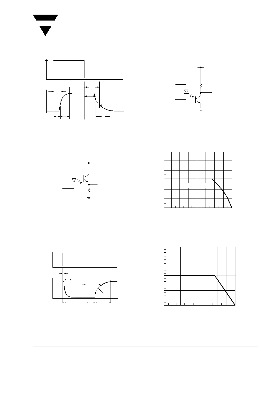
Fig. 1 Non-saturated Switching Timing
Fig. 2 Non-saturated Switching Timing
Fig. 3 Saturated Switching Timing
iild621_01
t
R
t
F
t
D
50%
t
PLH
V
O
I
F
t
PLH
t
S
iild621_02
VO
VCC = 5 V
RL = 75
F = 10 KHz,
DF = 50%
IF = 10 mA
iild621_03
IF
t
R
V
O
t
D
t
S
t
F
t
PHL
t
PLH
V
TH
= 1.5 V
Fig. 4 Saturated Switching Timing
Fig. 5 Maximum LED Current vs. Ambient Temperature
Fig. 6 Maximum LED Power Dissipation
iild621_04
VO
VCC = 5 V
RL
F = 10 KHz,
DF = 50%
-60
-40
-20
0
20
40
60
80
100
120
100
80
60
40
0
20
TA - Ambient Temperature - ∞C
I F
-
M
aximum
LED
Current
-
m
A
TJ (MAX) = 100 ∞C
iild621_05
iild621_06
-60 -40
-20
0
20
40
60
80
100
200
100
0
50
Ta - Ambient Temperature - ∞C
P
LED
-
LED
Power
-
m
W
150
