 | –≠–ª–µ–∫—Ç—Ä–æ–Ω–Ω—ã–π –∫–æ–º–ø–æ–Ω–µ–Ω—Ç: ILQ1615-1 | –°–∫–∞—á–∞—Ç—å:  PDF PDF  ZIP ZIP |
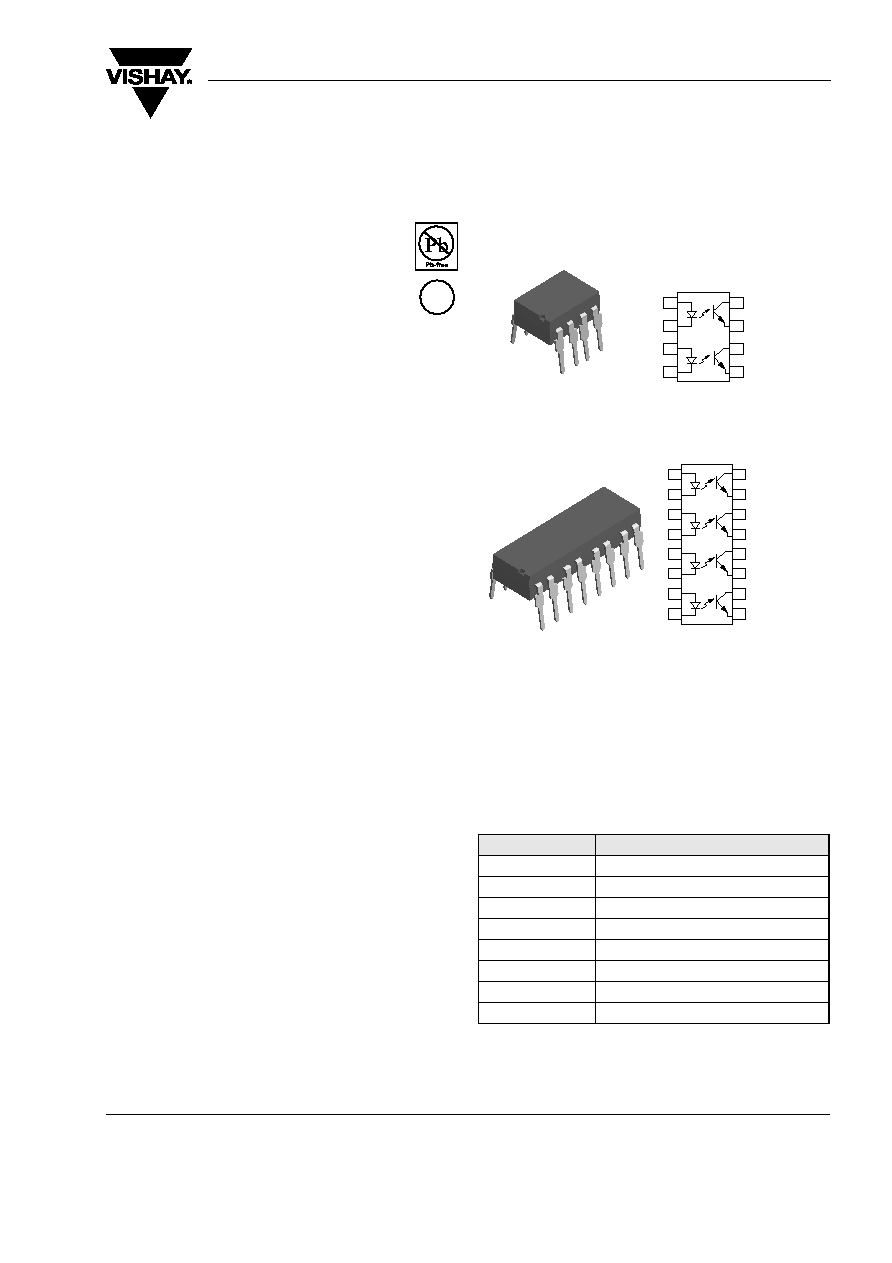
ILD1615/ ILQ1615
Document Number 82582
Rev. 1.5, 23-Mar-06
Vishay Semiconductors
www.vishay.com
1
i179052
1
2
3
4
8
7
6
5
E
C
C
E
A
C
C
A
A
C
C
A
A
C
C
A
E
C
C
E
E
C
C
E
16
15
14
13
12
11
10
9
1
2
3
4
5
6
7
8
Dual Channel
Quad Channel
Optocoupler, Phototransistor Output (Dual, Quad Channel),
110 ∞C Rated
Features
∑ Operating temperature from
- 55 ∞C to + 110 ∞C
∑ Identical Channel to Channel Footprint
∑ Dual and Quad Packages Feature:
- Reduced Board Space
- Lower Pin and Parts Count
- Better Channel to Channel CTR Match
- Improved Common Mode Rejection
∑ Isolation Test Voltage, 5300 V
RMS
∑ Lead (Pb)-free component
∑ Component in accordance to RoHS 2002/95/EC
and WEEE 2002/96/EC
Agency Approvals
∑ UL1577, File No. E52744 System Code H or J,
Double Protection
∑ CSA 93751
∑ BSI IEC60950 IEC60065
∑ DIN EN 60747-5-2 (VDE0884)
DIN EN 60747-5-5 pending
Available with Option 1
Description
The ILD/Q1615 are multi-channel 110 ∞C rated pho-
totransistor optocouplers that use GaAs IRLED emiters
and high gain NPN phototransistors. These devices are
constructed using over/under leadframe optical cou-
pling and double molded insulation technology result-
ing a withstand test voltage of 7500 VAC
PEAK
and a
working voltage of 1700 V
RMS
.
The binned min./max. and linear CTR characteristics
make these devices well suited for DC or AC voltage
detection. Eliminating the phototransistor base connec-
tion provides added electrical noise immunity from the
transients found in many industrial control environ-
ments.
Because of guaranteed maximum non-saturated and
saturated switching characteristics, the ILD/Q1615 can
be used in medium speed data I/O and control systems.
The binned min./max. CTR specification allow easy
worst case interface calculations for both level detec-
tion and switching applications. Interfacing with a
CMOS logic is enhanced by the guaranteed
CTR at I
F
= 1.0 mA.
Order Information
For additional information on the available options refer to
Option Information.
Part
Remarks
ILD1615-1
CTR 40 - 80 %, DIP-8
ILQ1615-1
CTR 40 - 80 %, DIP-16
ILD1615-2
CTR 63 - 125 %, DIP-8
ILQ1615-2
CTR 63 - 125 %, DIP-16
ILD1615-3
CTR 100 - 200 %, DIP-8
ILQ1615-3
CTR 100 - 200 %, DIP-16
ILD1615-4
CTR 160 - 320 %, DIP-8
ILQ1615-4
CTR 160 - 320 %, DIP-16
e3

www.vishay.com
2
Document Number 82582
Rev. 1.5, 23-Mar-06
ILD1615/ ILQ1615
Vishay Semiconductors
Absolute Maximum Ratings
T
amb
= 25 ∞C, unless otherwise specified
Stresses in excess of the absolute Maximum Ratings can cause permanent damage to the device. Functional operation of the device is
not implied at these or any other conditions in excess of those given in the operational sections of this document. Exposure to absolute
Maximum Rating for extended periods of the time can adversely affect reliability.
Input
Output
Coupler
Parameter
Test condition
Symbol
Value
Unit
Reverse voltage
V
R
6.0
V
Forward current
I
F
60
mA
Surge current
I
FSM
1.5
A
Power dissipation
P
diss
100
mW
Derate linearly from 25 ∞C
1.0
mW/∞C
Parameter
Test condition
Symbol
Value
Unit
Collector-emitter breakdown
voltage
BV
CEO
70
V
Emitter-collector breakdown
voltage
BV
ECO
7.0
V
Collector current
I
C
50
mA
t < 1.0 ms
I
C
100
mA
Power dissipation
P
diss
150
mW
Derate linearly from 25 ∞C
1.5
mW/∞C
Parameter
Test condition
Symbol
Value
Unit
Storage temperature
T
stg
- 55 to + 150
∞C
Operating temperature
T
amb
- 55 to + 110
∞C
Soldering temperature
2.0 mm distance from case
bottom
T
sld
260
∞C
Package power dissipation,
ILD1615
400
mW
Derate linearly from 25 ∞C
5.33
mW/∞C
Package power dissipation,
ILQ1615
500
mW
Derate linearly from 25 ∞C
6.67
mW/∞C
Isolation test voltage
t = 1.0 sec.
V
ISO
5300
V
RMS
Creepage
7.0
mm
Clearance
7.0
mm
Isolation resistance
V
IO
= 500 V, T
amb
= 25 ∞C
R
IO
10
12
V
IO
= 500 V, T
amb
= 100 ∞C
R
IO
10
11

ILD1615/ ILQ1615
Document Number 82582
Rev. 1.5, 23-Mar-06
Vishay Semiconductors
www.vishay.com
3
Electrical Characteristics
T
amb
= 25 ∞C, unless otherwise specified
Minimum and maximum values are testing requirements. Typical values are characteristics of the device and are the result of engineering
evaluation. Typical values are for information only and are not part of the testing requirements.
Input
Output
Coupler
Current Transfer Ratio
Parameter
Test condition
Symbol
Min
Typ.
Max
Unit
Forward voltage
I
F
= 10 mA
V
F
1.0
1.15
1.3
V
Breakdown voltage
I
R
= 10 µA
V
BR
6.0
30
V
Reverse current
V
R
= 6.0 V
I
R
0.01
10
µA
Capacitance
V
R
= 0 V, f = 1.0 MHz
C
O
25
pF
Parameter
Test condition
Symbol
Min
Typ.
Max
Unit
Collector-emitter capacitance
V
CE
= 5.0 V, f = 1.0 MHz
C
CE
6.8
pF
Collector-emitter leakage
current, -1, -2
V
CE
= 10 V
I
CEO
2.0
50
nA
Collector-emitter leakage, -3, -4 V
CE
= 10 V
I
CEO
5.0
100
nA
Collector-emitter breakdown
voltage
I
CE
= 0.5 mA
BV
CEO
70
V
Emitter-collector breakdown
voltage
I
E
= 0.1 mA
BV
ECO
7.0
V
Package transfer characteristics
Channel/Channel CTR match
I
F
= 10 mA, V
CE
= 5.0 V
CTRX/
CTRY
1 to 1
2 to 1
Parameter
Test condition
Symbol
Min
Typ.
Max
Unit
Capacitance (input-output)
V
IO
= 0 V, f = 1.0 MHz
C
IO
0.8
pF
Insulation resistance
V
IO
= 500 V, T
A
= 25 ∞C
R
S
10
12
10
14
Channel to channel isolation
500
VAC
Parameter
Test condition
Part
Symbol
Min
Typ.
Max
Unit
Current Transfer Ratio
(collector-emitter saturated)
I
F
= 10 mA, V
CE
= 0.4 V
ILD1615-1
ILQ1615-1
CTR
CEsat
25
%
ILD1615-2
ILQ1615-2
CTR
CEsat
40
%
ILD1615-3
ILQ1615-3
CTR
CEsat
60
%
ILD1615-4
ILQ1615-4
CTR
CEsat
100
%

www.vishay.com
4
Document Number 82582
Rev. 1.5, 23-Mar-06
ILD1615/ ILQ1615
Vishay Semiconductors
Switching Characteristics
Non-saturated
Saturated
Current Transfer Ratio
(collector-emitter)
I
F
= 10 mA, V
CE
= 5.0 V
ILD1615-1
ILQ1615-1
CTR
CE
40
60
80
%
I
F
= 1.0 mA, V
CE
= 5.0 V
ILD1615-1
ILQ1615-1
CTR
CE
13
30
%
I
F
= 10 mA, V
CE
= 5.0 V
ILD1615-2
ILQ1615-2
CTR
CE
63
80
125
%
I
F
= 1.0 mA, V
CE
= 5.0 V
ILD1615-2
ILQ1615-2
CTR
CE
22
45
%
I
F
= 10 mA, V
CE
= 5.0 V
ILD1615-3
ILQ1615-3
CTR
CE
100
150
200
%
I
F
= 1.0 mA, V
CE
= 5.0 V
ILD1615-3
ILQ1615-3
CTR
CE
34
70
%
I
F
= 10 mA, V
CE
= 5.0 V
ILD1615-4
ILQ1615-4
CTR
CE
160
200
320
%
I
F
= 1.0 mA, V
CE
= 5.0 V
ILD1615-4
ILQ1615-4
CTR
CE
56
90
%
Parameter
Test condition
Symbol
Min
Typ.
Max
Unit
Turn-on time
I
F
= 10 mA, V
CC
= 5.0 V, R
L
= 75
,
50 % of V
PP
t
on
3.0
µs
Rise time
I
F
= 10 mA, V
CC
= 5.0 V, R
L
= 75
,
50 % of V
PP
t
r
2.0
µs
Turn-off time
I
F
= 10 mA, V
CC
= 5.0 V, R
L
= 75
,
50 % of V
PP
t
off
2.3
µs
Fall time
I
F
= 10 mA, V
CC
= 5.0 V, R
L
= 75
,
50 % of V
PP
t
f
2.0
µs
Propagation H-L
I
F
= 10 mA, V
CC
= 5.0 V, R
L
= 75
,
50 % of V
PP
t
PHL
1.1
µs
Propagation L-H
I
F
= 10 mA, V
CC
= 5.0 V, R
L
= 75
,
50 % of V
PP
t
PLH
2.5
µs
Parameter
Test condition
Part
Symbol
Min
Typ.
Max
Unit
Turn-on time
I
F
= 20 mA, V
CC
= 5.0 V, R
L
= 1.0 k
,
V
HT
1.5 V
ILD1615-1
ILQ1615-1
t
on
3.0
µs
I
F
= 10 mA, V
CC
= 5.0 V, R
L
= 1.0 k
,
V
HT
1.5 V
ILD1615-2
ILQ1615-2
t
on
4.3
µs
ILD1615-3
ILQ1615-3
t
on
4.3
µs
I
F
= 5.0 mA, V
CC
= 5.0 V, R
L
= 1.0 k
,
V
HT
1.5 V
ILD1615-4
ILQ1615-4
t
on
6.0
µs
Rise time
I
F
= 20 mA, V
CC
= 5.0 V, R
L
= 1.0 k
,
V
HT
1.5 V
ILD1615-1
ILQ1615-1
t
r
2.0
µs
I
F
= 10 mA, V
CC
= 5.0 V, R
L
= 1.0 k
,
V
HT
1.5 V
ILD1615-2
ILQ1615-2
t
r
2.8
µs
ILD1615-3
ILQ1615-3
t
r
2.8
µs
I
F
= 5.0 mA, V
CC
= 5.0 V, R
L
= 1.0 k
,
V
HT
1.5 V
ILD1615-4
ILQ1615-4
t
r
4.6
µs
Parameter
Test condition
Part
Symbol
Min
Typ.
Max
Unit

ILD1615/ ILQ1615
Document Number 82582
Rev. 1.5, 23-Mar-06
Vishay Semiconductors
www.vishay.com
5
Common Mode Transient Immunity
Turn-off time
I
F
= 20 mA, V
CC
= 5.0 V, R
L
= 1.0 k
,
V
HT
1.5 V
ILD1615-1
ILQ1615-1
t
off
18
µs
I
F
= 10 mA, V
CC
= 5.0 V, R
L
= 1.0 k
,
V
HT
1.5 V
ILD1615-2
ILQ1615-2
t
off
25
µs
ILD1615-3
ILQ1615-3
t
off
25
µs
I
F
= 5.0 mA, V
CC
= 5.0 V, R
L
= 1.0 k
,
V
HT
1.5 V
ILD1615-4
ILQ1615-4
t
off
25
µs
Fall time
I
F
= 20 mA, V
CC
= 5.0 V, R
L
= 1.0 k
,
V
HT
1.5 V
ILD1615-1
ILQ1615-1
t
f
11
µs
I
F
= 10 mA, V
CC
= 5.0 V, R
L
= 1.0 k
,
V
HT
1.5 V
ILD1615-2
ILQ1615-2
t
f
14
µs
ILD1615-3
ILQ1615-3
t
f
14
µs
I
F
= 5.0 mA, V
CC
= 5.0 V, R
L
= 1.0 k
,
V
HT
1.5 V
ILD1615-4
ILQ1615-4
t
f
15
µs
Propagation H-L
I
F
= 5.0 mA, V
CC
= 5.0 V, R
L
= 1.0 k
,
V
HT
1.5 V
ILD1615-1
ILQ1615-1
t
PHL
1.6
µs
ILD1615-2
ILQ1615-2
t
PHL
2.6
µs
ILD1615-3
ILQ1615-3
t
PHL
2.6
µs
ILD1615-4
ILQ1615-4
t
PHL
5.4
µs
Propagation L-H
I
F
= 5.0 mA, V
CC
= 5.0 V, R
L
= 1.0 k
,
V
HT
1.5 V
ILD1615-1
ILQ1615-1
t
PLH
8.6
µs
ILD1615-2
ILQ1615-2
t
PLH
7.2
µs
ILD1615-3
ILQ1615-3
t
PLH
7.2
µs
ILD1615-4
ILQ1615-4
t
PLH
7.4
µs
Parameter
Test condition
Symbol
Min
Typ.
Max
Unit
Common mode rejection output
high
V
CM
= 50 V
P-P
, R
L
= 1.0 k
,
I
F
= 0 mA
CM
H
5000
V/µs
Common mode rejection output
low
V
CM
= 50 V
P-P
, R
L
= 1.0 k
,
I
F
= 10 mA
CM
L
5000
V/µs
Common mode coupling
capacitance
C
CM
0.01
pF
Parameter
Test condition
Part
Symbol
Min
Typ.
Max
Unit