 | –≠–ª–µ–∫—Ç—Ä–æ–Ω–Ω—ã–π –∫–æ–º–ø–æ–Ω–µ–Ω—Ç: JAN-03 | –°–∫–∞—á–∞—Ç—å:  PDF PDF  ZIP ZIP |
VISHAY
Document Number 84067
Rev. 7, 07-Jan-03
Vishay Semiconductors
www.vishay.com
1
Basic Definitions
Basic Sinterglass Diode Parameters
The major parameters for the selection of the appro-
priate sinterglass diodes are the maximum reverse
voltage (V
RRM
), the average forward current (I
FAV
)
and for switching application the reverse recovery
characteristic (t
rr
), too. Additional parameters may be
for example the reverse avalanche energy capability
(E
R
) and forward surge capability (I
FSM
) etc.
V
R
Reverse voltage
V
RRM
Repetitive peak reverse voltage, including all repeated reverse transient voltages
V
(BR)R
Reverse breakdown voltage
I
R
Reverse (leakage) current, at a specified reverse voltage V
R
and temperature T
J
I
F
Forward current
V
F
Forward voltage drop, at a specified forward current I
F
and temperature T
J
I
FAV
Average forward output current, at a specified current waveform (normally 10ms/50Hz half-sine-
wave, sometimes 8.3ms/60Hz half-sine-wave), a specified reverse voltage and a specified mounting
condition (e.g. lead-length = 10mm or PCB mounted with certain pads and distance)
I
FSM
Peak forward surge current, with a specified current waveform (normally 10ms/50Hz half-sine-wave,
sometimes 8.3ms/60Hz half-sine-wave),
t
rr
Reverse recovery time, at a specified forward current (normally 0.5A), a specified reverse current
(normally 1.0A) and specified measurement conditions (normally from 0 to 0.25A)
E
R
Reverse avalanche energy, non-repetitive
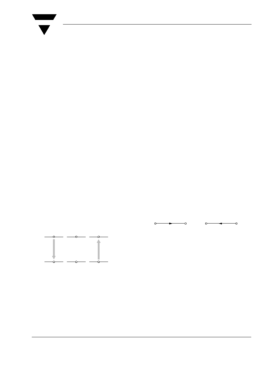
Polarity Conventions
The voltage direction is given
∑ by an arrow which points from the measuring point
to the reference point
or
∑ by a two letter subscript, where the first letter is the
measuring point and the second letter is the refer-
ence point.
The numerical value of the voltage is positive if the
potential at the arrow tail is higher than at the arrow
head; i.e., the potential difference from the measuring
point (A) to the reference point (B) is positive.
The numerical value of the voltage is negative if the
potential at the arrow head is higher than the tail; i.e.,
the potential difference from the measuring point to
the reference point is negative.
In the case of alternating voltages, once the voltage
direction is selected it is maintained throughout. The
alternating character of the quantity is given with the
time dependent change in sign of its numerical values
.
The numerical value of the current is positive if the
charge of the carriers moving in the direction of the
arrow is positive (conventional current direction), or if
the charge of the carriers moving against this direc-
tion is negative. The numerical value of the current is
negative if the charge of the carriers moving in the
direction of the arrow is negative, or if the charge of
the carriers moving against this direction is positive.
The general rules stated above are also valid for alter-
nating quantities. Once the direction is selected, it is
maintained throughout. The alternating character of
the quantity is given with the time-dependent change
in sign of its numerical values.
Figure 1.
A
B
V
1
A
B
A
B
V
AB
V
2
=≠V
1
=V
BA
=≠V
AB
94 9315
Figure 2.
A
B
A
B
I
1
I
2
= ≠I
1
94 9316

www.vishay.com
2
Document Number 84067
Rev. 7, 07-Jan-03
VISHAY
Vishay Semiconductors
Polarity conventions for diodes
Here, the direction of arrows is selected in such a way
that the numerical values of currents and voltages are
positive both for forward (F or f) and reverse (R or r)
directions.
Arrangement of Symbols
Letter symbols for current, voltage and power
(according to DIN 41 785, sheet 1)
To represent current, voltage and power, a system of
basic letter symbols is used. Capital letters are used
for the representation of peak, mean, DC or root-
mean-square values. Lower case letters are used for
the representation of instantaneous values which
vary with time.
Capital letters are used as subscripts to represent
continuous or total values, while lower case letters are
used to represent varying values.
The following table summarizes the rules given above
.
Letter symbols for impedance, admittances, two-
port parameters etc.
For impedance, admittance, two-port parameters,
etc. capital letters are used for the representation of
external circuits of which the device is only a part.
Lower case letters are used for the representation of
electrical parameters inherent in the device.
CAPITAL letters are used as subscripts for the desig-
nation of static (DC) values, while lower case letters
are used for the designation of small-signal values.
If more than one subscript is used (h
FE
, h
fe
), the letter
symbols are either all capital or all lower case.
If the subscript has numeric (single, double, etc.) as
well as letter symbol(s) (such as h
21E
or h
21e'
), the dif-
ferentiation between static and small-signal value is
made only by a subscript letter symbol.
Other quantities (values) which deviate from the
above rules are given in the list of letter symbols.
The following table summarizes the rules given above
.
Examples:
G
P
Power gain
Z
S
Source impedance
f
T
Transition frequency
I
F
Forward current
Example for the use of symbols
according to 41785 and IEC 148
V
F
Forward voltage
V
R
Reverse voltage
V
FSM
Surge forward voltage (non-repetitive)
Figure 3.
Basic letter
Upper-case
Upper-case
Instantaneous values which
vary with time
Maximum (peak) average
(mean) continuous (DC) or
root-mean-square (RMS)
values
Subscript(s)
Upper-case
Upper-case
Varying component alone, i.e.,
instantaneous,
root-mean-square, maximum
or average values
Continuous (without signal) or
total (instantaneous, average or
maximum) values
A
I
F
K
A
I
R
K
V
F
V
R
Basic letter
Upper-case
Upper-case
Electrical parameters inherent
in the semiconductor devices
except inductances and
capacitances
Electrical parameters of
external circuits and of circuits
in which the semiconductor
device forms only a part; all
inductances and capacitances
Subscript(s)
Upper-case
Upper-case
Small-signal values
Static (dc) values
Figure 4.
V
FWM
V
FSM
t
V
F
V
RSM
V
RRM
V
RWM
V
R
0
93 7796
V
FRM

VISHAY
Document Number 84067
Rev. 7, 07-Jan-03
Vishay Semiconductors
www.vishay.com
3
V
RSM
Surge reverse voltage (non-repetitive)
V
FRM
Repetitive peak forward voltage
V
RRM
Repetitive peak reverse voltage
V
FWM
Crest working forward voltage
V
RWM
Crest working reverse voltage
List of Symbols
A
Anode
a
Distance (in mm)
b
pn
Normalized power factor
C
Capacitance, general
C
case
Case capacitance
C
D
Diode capacitance
C
i
Junction capacitance
C
L
Load capacitance
C
P
Parallel capacitance
E
R
Reverse avalanche energy, non-repetitive
F
Noise figure
f
Frequency
f
g
Cut-off-frequency
g
Conductance
K
Kelvin, absolute temperature
I
F
Forward current
i
F
Forward current, instantaneous total value
I
FAV
Average forward current, rectified current
I
FRM
Repetitive peak forward current
I
FSM
Surge forward current, non-repetitive
I
FWM
Crest working forward current
I
R
Reverse current
I
RM
Maximum reverse current
i
R
Reverse current, instantaneous total value
I
RAV
Average reverse current
I
RRM
Repetitive peak reverse current
I
RSM
Non-repetitive peak reverse current
I
RWM
Crest working reverse current
I
S
Supply current
I
Z
Z-operating current
I
ZM
Z-maximum current
l
Length (in mm), (case-holder/soldering point)
LOCEP (local epitaxy)
A registrated trade mark of TEMIC for a pro-
cess of epitaxial deposition on silicon. Applica-
tions occur in planer Z-diodes. It has an
advantage compared to the normal process,
with improved reverse current.
P
Power
P
R
Reverse Power
P
tot
Total power dissipation
P
V
Power dissipation, general
Pvp
Pulse-power dissipation
Q
Quality
Q
rr
Reverse recovery charge
R
F
Forward resistance
r
f
Differential forward resistance
R
L
Load resistor
r
P
Parallel resistance, damping resistance
R
R
Reverse resistance
r
r
Differential reverse resistance
r
s
Series resistance
R
thJA
Thermal resistance between junction and
ambient
R
thJC
Thermal resistance between junction and case
R
thJL
Thermal resistance junction lead
r
z
Differential Z-resistance in breakdown region
(range) r
z
= r
zj
+ r
zth
r
zj
Z-resistance at constant junction temperature,
inherent Z-resistance
r
zth
Thermal part of the Z-resistance
T
Temperature, measured in centigrade
T
Absolute temperature, Kelvin temperature
T
Period duration
T
amb
Ambient temperature (range)
t
av
Integration time
T
case
Case temperature
t
fr
Forward recovery time
T
j
Junction temperature
T
K
Temperature coefficient
T
L
Connecting lead temperature in the holder (sol-
dering point) at the distance/(mm) from case
t
P
Pulse duration (time)
Duty cycle
t
r
Rise time
t
rr
Reverse recovery time
t
s
Storage time
T
sd
Soldering temperature
T
stg
Storage temperature (range)
V
(BR)
Breakdown voltage
VF
Forward voltage
V
F
Forward voltage, instantaneous total value
V
FAV
Average forward voltage
V
o
Rectified voltage
V
FP
Turn on transient peak voltage
t
p
T
----

www.vishay.com
4
Document Number 84067
Rev. 7, 07-Jan-03
VISHAY
Vishay Semiconductors
V
FSM
Surge forward voltage, non-repetitive
V
FRM
Repetitive peak forward voltage
V
FWM
Crest working forward voltage
V
HF
RF voltage, RMS value
V
HF
RF voltage, peak value
V
R
Reverse voltage
V
R
Reverse voltage, instantaneous total value
V
RSM
Surge reverse voltage, non-repetitive
V
RRM
Repetitive peak reverse voltage
V
RWM
Crest working reverse voltage
V
S
Supply voltage
V
T
Temperature voltage
V
Z
Z-operating voltage
Z
thp
Thermal resistance - pulse operation
Angle of current flow
r
Rectification efficiency
T
o
Time constant
C
D
Capacitance deviation
Data Sheet Construction
Data sheet information is generally presented in the
following sequence:
∑ Device description
∑ Absolute maximum ratings
∑ Thermal data - thermal resistances
∑ Characteristics, switching characteristics
∑ Electrical characteristics
∑ Dimensions (mechanical data)
Additional information on device performance is pro-
vided where necessary.
Device Description
The following information is provided: part number,
semiconductor materials used, sequence of zones,
technology used, device type and, if necessary con-
struction.
Also, information on the typical Applications and spe-
cial Features is given
Absolute Maximum Ratings
The absolute maximum ratings indicate the maximum
permissible operational and environmental condi-
tions. Exceeding any one of these conditions could
result in the destruction of the device. Unless other-
wise specified, an ambient temperature of 25∞C
±
3∞C is assumed for all absolute maximum ratings.
Most absolute ratings are static characteristics; if they
are measured by a pulse method, the associated
measurement conditions are stated.
Maximum ratings are absolute
(i.e., not interdependent).
Any equipment incorporating semiconductor devices
must be designed so that even under the most unfa-
vorable operating conditions the specified maximum
ratings of the devices used are never exceeded.
These ratings could be exceeded because of
changes in:
∑ Supply voltage
∑ The properties of other components used in the
equipment
∑ Control settings
∑ Load conditions
∑ Drive level
∑ Environmental conditions
∑ The properties of the devices themselves (aging)
Thermal Data - Thermal Resistances
Some thermal data (e.g., junction temperature, stor-
age temperature range, total power dissipation),
impose a limit on the application range of the device,
and are given under the heading "Absolute Maximum
Ratings".
A special section is provided for thermal resistances.
Temperature coefficients, on the other hand, are
listed together with the associated parameters under
,,Characteristics, Switching Characteristics".
Characteristics, Switching Characteristics
Under this heading, the most important operational
electrical characteristics (minimum, typical and maxi-
mum values) are grouped together with associated
test conditions supplemented with graphs.
Dimensions (Mechanical Data)
Important dimensions and the sequence of connec-
tions supplemented by a circuit diagram are included
in the mechanical data. Case outline drawings carry
DIN, JEDEC or commercial designations. Information
on weight complete is also included.
Note:
If the dimension information does not include any tol-
erances, then lead length and mounting hole dimen-
sions are minimum values. All other dimensions are
maximum.

VISHAY
Document Number 84067
Rev. 7, 07-Jan-03
Vishay Semiconductors
www.vishay.com
5
Additional Information
Not for new developments: This heading indicates
that the device concerned should not be used in
equipment under development. It is, however, avail-
able for devices presently in production.