 | –≠–ª–µ–∫—Ç—Ä–æ–Ω–Ω—ã–π –∫–æ–º–ø–æ–Ω–µ–Ω—Ç: LH1532AAC | –°–∫–∞—á–∞—Ç—å:  PDF PDF  ZIP ZIP |

Document Number: 83829
www.vishay.com
Revision 17-August-01
3≠134
FEATURES
∑ Dual Channel (LH1540)
∑ Current Limit Protection
∑ l/O Isolation, 5300 V
RMS
∑ Typical
R
ON
20
∑ Load Voltage 350 V
∑ Load Current 120 mA
∑ High Surge Capability
∑ Linear, AC/DC Operation
∑ Clean Bounce Free Switching
∑ Low Power Consumption
∑ SMD Lead Available on Tape and Reel
AGENCY APPROVALS
∑ UL ≠ File No. E52744
∑ CSA ≠ Certification 093751
∑ BSI/BABT Cert. No. 7980
∑ VDE 0884 Approval
∑ FIMKO Approval
APPLICATIONS
∑ General Telecom Switching
≠ On/off Hook Control
≠ Ring Delay
≠ Dial Pulse
≠ Ground Start
≠ Ground Fault Protection
∑ Instrumentation
∑ Industrial Controls
DESCRIPTION
The LH1532 dual 1 Form A relays are SPST normally
open switches that can replace electromechanical
relays in many applications. They are constructed using
a GaAIAs LED for actuation control and an integrated
monolithic die for the switch output. The die, fabricated
in a high-voltage dielectrically isolated technology is
comprised of a photodiode array, switch control cir-
cuitry, and MOSFET switches. In addition, the LH1532
SSRs employ current-limiting circuitry, enabling them to
pass FCC 68.302 and other regulatory surge require-
ments when overvoltage protection is provided.
Part Identification
Part Number
Description
LH1532AB
8-pin DIP, Tubes
LH1532AAC
8-pin SMD, Gullwing, Tubes
LH1532AACTR
8-pin SMD, Gullwing, Tape and Reel
pin one ID
.268 (6.81)
.255 (6.48)
.390 (9.91)
.379 (9.63)
.045 (1.14)
.030 (0.76)
4
∞ typ.
.100 (2.54) typ.
10
∞
3
∞≠9∞
.300 (7.62)
typ.
.022 (.56)
.018 (.46)
.012 (.30)
.008 (.20)
.130 (3.30)
.110 (2.79)
.150 (3.81)
.130 (3.30)
.035 (.89)
.020 (.51)
.250 (6.35)
.230 (5.84)
4
3
2
1
.031 (0.79)
.050 (1.27)
5
6
7
8
Pin one I.D.
.390 (9.91)
.379 (9.63)
.045 (1.14)
.030 (0.78)
.040 (1.02)
.020 (.51)
4
∞
typ.
.008 (.25)
.004 (.10)
.150 (3.81)
.130 (3.30)
.100 (2.54)
typ.
.050
(1.27)
typ.
.312 (7.80)
.298 (7.52)
.315
(8.00)
typ.
.395 (10.03)
.375 (9.52)
.031 (.79)
typ.
.268 (6.81)
.255 (6.48)
Radius
.010
(2.54)
typ.
10
∞
3
∞
to 7
∞
Package Dimensions in Inches (mm)
DIP
SMD
8
7
6
5
1
2
3
4
S2'
S2'
S2
S2
S1
S1
S1'
S1'
LH1532AB/AAC/AACTR
Dual 1 Form A
Solid State Relay

Document Number: 83829
www.vishay.com
Revision 17-August-01
3≠135
Absolute Maximum Ratings,
T
A
=25
∞
C
Stresses in excess of the absolute Maximum Ratings can cause permanent
damage to the device. These are absolute stress ratings only. Functional oper-
ation of the device is not implied at these or any other conditions in excess of
those given in the operational sections of this document. Exposure to absolute
Maximum Ratings for extended periods of time can adversely affect reliability.
Ambient Temperature Range (
T
A
) .................................... ≠40 to +85
∞
C
Storage Temperature Range (
T
stg
) ................................. ≠40 to +150
∞
C
Pin Soldering Temperature (t=10 s max) (
T
S
) ............................. 260
∞
C
Input/Output Isolation Voltage
(t=1.0 s) (
V
ISO
)................................................................... 5300 V
RMS
Pole-to-Pole Isolation Voltage (S1 to S2)*
(dry air, dust free, at sea level) ................................................. 1600 V
LED Continuous Forward Current (
I
F
) .........................................50 mA
LED Reverse Voltage (
I
R
10
µ
A) (
V
R
) ........................................... 8.0 V
DC or Peak AC Load Voltage (
I
L
50
µ
A) (
V
L
) .............................. 350 V
Continuous DC Load Current (
I
L
)
One Pole Operating.................................................................120 mA
Two Poles Operating ...............................................................110 mA
Peak Load Current (t=100 ms) (single shot) (
I
P
) ................................
Output Power Dissipation (continuous) (
P
DISS
)........................ 600 mW
*
Breakdown occurs between the output pins external to the package.
Refer to Current Limit Performance Application Note for a discussion on
relay operation during transient currents.
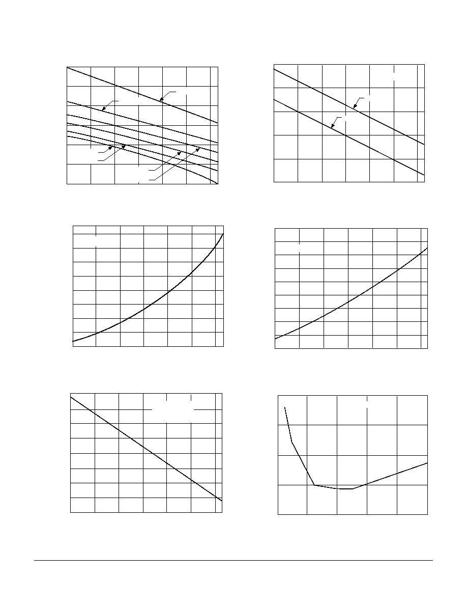
Recommended Operating Conditions
60
80
0
40
120
100
20
≠40 ≠20 0 20 40 60 80
Load Current (mA)
Ambient Temperature (
∞C)
I
Fon
=2.0 mA
I
Fon
=3.0 mA
I
Fon
=4.0 mA
I
Fon
=5.0 to 20 mA
Electrical Characteristics,
T
A
=25
∞
C
Minimum and maximum values are testing requirements. Typical values are characteristics of the device and are the result of
engineering evaluations. Typical values are for information only and are not part of the testing requirements.
Parameter
Sym.
Min.
Typ.
Max.
Units
Test Conditions
Input
LED Forward Current, Switch Turn-on
I
Fon
--
1.0
2.0
mA
I
L
=100 mA, t=10 ms
LED Forward Current, Switch Turn-off
I
Foff
0.2
0.9
--
mA
V
L
±300 V
LED Forward Voltage
V
F
1.15
1.26
1.45
V
I
F
=10 mA
Output
ON-resistance
R
ON
12
20
25
I
F
=5.0 mA,
I
L
=50 mA
OFF-resistance
R
OFF
0.5
5000
--
G
I
F
=0 mA,
V
L
=±100 V
Current Limit
I
LMT
170
210
250
mA
I
F
=5.0 mA, t=5.0 ms
V
L
=±6.0 V
Off-state Leakage Current
--
--
0.02
200
nA
I
F
=0 mA,
V
L
=±100 V
--
--
1.0
µ
A
I
F
=0 mA,
V
L
=±350 V
Output Capacitance
--
--
55
--
pF
I
F
=0 mA,
V
L
=1.0 V
--
10
--
I
F
=0 mA,
V
L
=50 V
Pole-to-Pole Capacitance (S1 to S2)
--
--
0.5
--
pF
I
F
=5.0 mA
Switch Offset
--
--
0.15
--
V
I
F
=5.0 mA
Transfer
Input/Output Capacitance
C
ISO
--
1.1
--
pF
V
ISO
=1.0 V
Turn-on Time
t
on
--
1.4
2.5
ms
I
F
=5.0 mA,
I
L
=50 mA
Turn-off Time
t
off
--
0.7
2.5
ms
I
F
=5.0 mA,
I
L
=50 mA
Document Number: 83829
www.vishay.com
Revision 17-August-01
3≠136
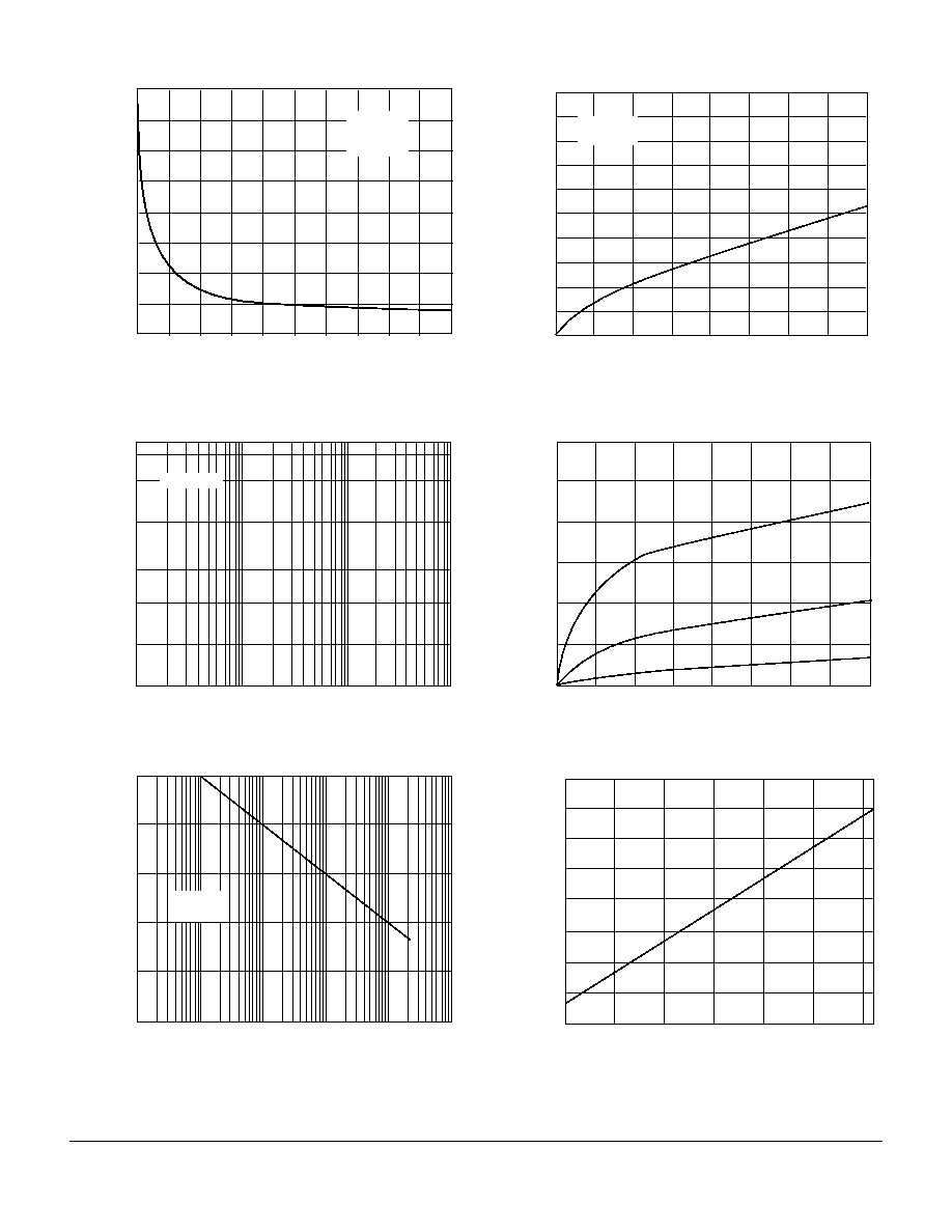
Typical Performance Characteristics
Figure 1. LED Voltage vs. Temperature
Figure 2. LED Current for Switch Turn-on vs. Temperature
Figure 3. Current Limit vs. Temperature
Ambient Temperature (
∞C)
LED Forward Voltage (V)
≠40
≠20
0
20
40
60
80
1.6
1.5
1.4
1.3
1.2
1.1
1.0
I
F
=1.0 mA
I
F
=20 mA
I
F
=50 mA
I
F
=2.0 mA
I
F
=5.0 mA
I
F
=10 mA
Ambient Temperature (
∞C)
100
≠60
80
60
40
≠40
≠40
20
≠20
0
≠20
0
20
40
60
80
I
L
= 100 mA
LED Forward Current for Switch
Turn-on (%), Normalized to 25
∞
C
≠40
40
10
30
20
0
≠20
≠10
≠40
≠30
≠20
0
20
40
60
Ambient Temperature (
∞C)
80
I
F
= 5.0 mA
t = 5.0 ms
V
L
=
SEE ELEC. CHAR
.
Change in Current Limit (%)
Normalized to 25
∞
C
Figure 4. LED Dropout Voltage vs. Temperature
Figure 5. On-resistance vs. Temperature
Figure 6. Variation in On-resistance vs. LED Current
≠40
0
20
Ambient Temperature (
∞C)
1.20
1.15
1.10
0.95
1.00
40
1.05
80
60
≠20
MIN.
TYP.
I
L
= 100 mA
LED Forward Voltage (V)
≠40
50
10
30
20
40
≠20
≠30
≠10
≠40
0
≠20
0
20
40
60
80
Ambient Temperature (
∞C)
I
L
= 50 mA
Change in ON-resistance (%)
Normalized to 25
∞
C
0
1.5
0.5
≠0.5
1.0
0
4
8
12
LED Forward Current (mA)
16
20
I
L
= 50 mA
ac/dc On-resistance Variation (%)
Normalized to Data Sheet
R
ON
Specification at I
F
=5.0 mA
Document Number: 83829
www.vishay.com
Revision 17-August-01
3≠137
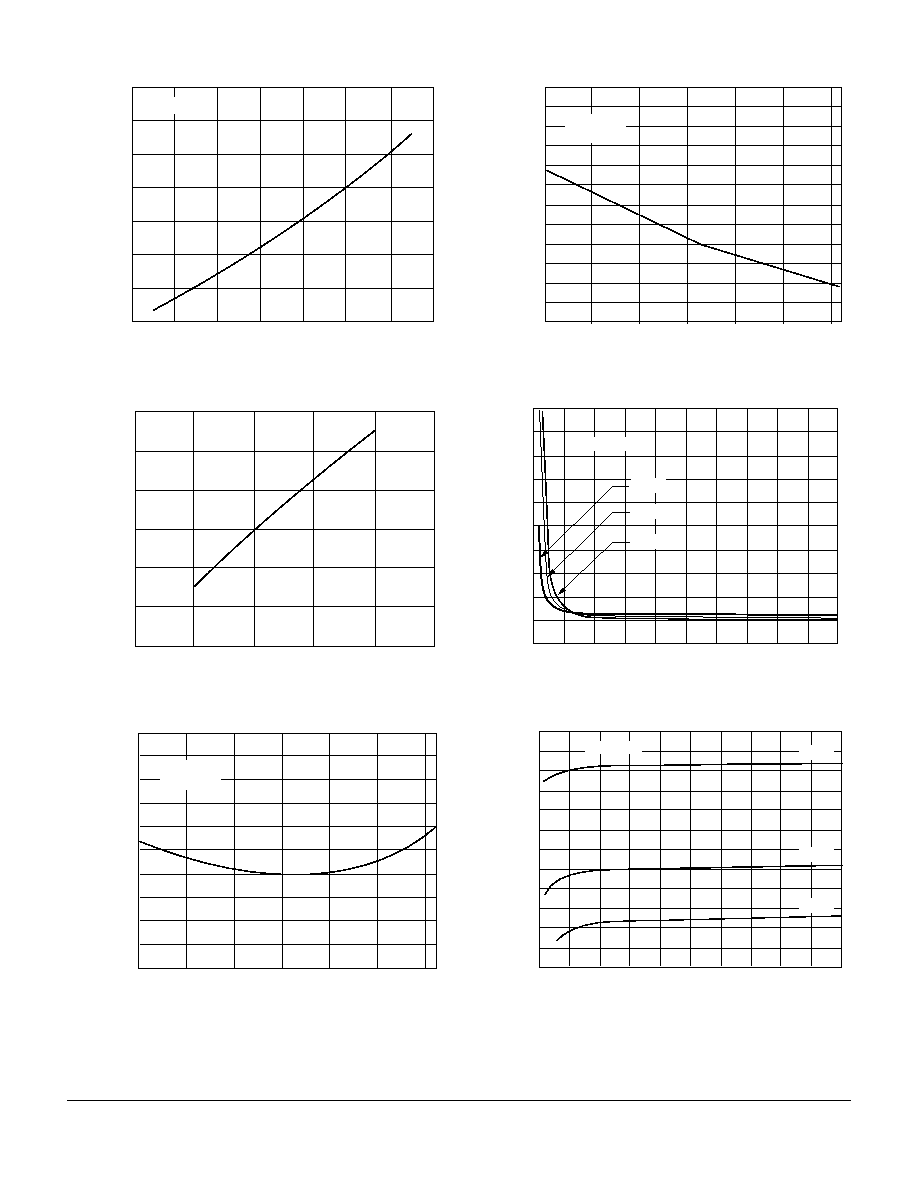
Figure 7. Switch Capacitance vs. Applied Voltage
Figure 8. Insertion Loss vs. Frequency
Figure 9. Output Isolation
0
20
40
Applied Voltage (V)
80
50
70
60
40
20
0
10
60
30
100
80
I
F
=0 mA
T
A
=25
∞C
f=1.0 MHz
Capacitance (pF)
Frequency (Hz)
0.30
0
0.25
0.20
0.10
0.05
10
2
10
3
10
4
10
5
0.15
R
L
= 600
Insertion Loss (dB)
Frequency (Hz)
100
80
60
40
20
0
10
2
10
3
10
4
10
5
10
6
10
7
Isolation (dB)
V
P
=10 V
R
L
=50
Figure 10. Leakage Current vs. Applied Voltage
Figure 11. Leakage Current vs. Applied Voltage at Elevated
Temperatures
Figure 12. Switch Breakdown Voltage vs. Temperature
90
0
50
100
150
200
250
300
Load Voltage (V)
100
70
80
60
40
30
50
20
10
0
350
400
I
F
= 0 mA
T
A
= 25
∞C
Off-state Leakage Current (pA)
Load Voltage (V)
3.0
2.5
2.0
1.0
0.5
1.5
0
0
50
100
150
200
250
300
350
400
85
∞C
70
∞C
50
∞C
Off-state Leakage Current (nA)
≠40
≠20
0
20
40
60
80
Ambient Temperature (
∞C)
8
0
4
2
6
≠2
≠6
≠8
≠4
Change in Breakdown Voltage (%)
Normalized to 25
∞
C
Document Number: 83829
www.vishay.com
Revision 17-August-01
3≠138
Figure 13. Switch Offset Voltage vs. Temperature
Figure 14. Switch Offset Voltage vs. LED Current
Figure 15. Turn-on Time vs. Temperature
20
40
Ambient Temperature (
∞C)
3.5
0
50
70
60
30
3.0
1.5
2.0
2.5
0.5
1.0
80
90
I
F
= 5.0 mA
Switch Offset Voltage (
µ
V)
0
10
LED Forward Current (mA)
0.6
0
15
25
20
5
0.5
0.2
0.3
0.4
0.1
Switch Offset Voltage (
µ
V)
≠40
≠20
0
20
40
60
80
Ambient Temperature (
∞C)
60
50
≠20
≠30
≠10
0
10
20
30
40
≠40
I
F
=5.0 mA
I
L
=50 mA
Change in Turn-on Time (%)
Normalized to 25
∞
C
Figure 16. Turn-off Time vs. Temperature
Figure 17. Turn-on Time vs. LED Current
Figure 18. Turn-off Time vs. LED Current
120
40
≠40
100
80
60
20
≠20
≠60
0
≠40
≠20
0
20
40
60
80
≠80
160
140
Ambient Temperature (
∞C)
I
F
=5.0 mA
I
L
=50 mA
Change in Turn-off Time (%)
Normalized to 25
∞
C
0
10
20
LED Forward Current (mA)
10
8
6
0
2
30
4
50
40
≠40
∞C
I
L
=50 mA
Turn-on Time (ms)
25
∞C
85
∞C
0
10
20
1.4
1.2
1.0
0.2
30
50
40
0.8
0.6
0.4
I
L
=50 mA
LED Forward Current (mA)
≠40
∞C
25
∞C
85
∞C
Turn-off Time (ms)