
Document Number: 83830
www.vishay.com
Revision 17-August-01
3≠139
LH1532FP/FPTR
Dual 1 Form A
Solid State Relay
FEATURES
∑ Two Independent Relays in a Single Package
∑ Package--
FLAT PAK
∑ l/O Isolation, 3000 V
RMS
∑ Solid-state Relay (Equivalent to AQW210S)
≠ Typical
R
ON
20
≠ Load Voltage 350 V
≠ Load Current 120 mA
≠ Current Limit Protection
≠ High Surge Capability
≠ Linear, AC/DC Operation
≠ Clean Bounce Free Switching
≠ Low Power Consumption
≠ High Reliability Monolithic Receptor
AGENCY APPROVALS
∑ UL ≠ File No. E52744
APPLICATIONS
∑ General Telecom Switching
≠ On/off Hook Control
≠ Ring Relay
≠ Ground Start
∑ Industrial Controls
≠ Triac Predriver
≠ Output Modules
∑ Peripherals
≠ Transducer Driver
∑ Instrumentation
≠ Automatic Tuning/Balancing
≠ Flying Capacitor
≠ Analog Multiplexing
∑ See Application Note 56
DESCRIPTION
The LH1532FP is a Dual 1 Form A (SPST) which can
replace electromechanical relays in many applications.
They are constructed using a GaAlAs LED for activation
control and an integrated monolithic die for the switch
output. The die is comprised of a photodiode array,
switch control circuity and MOSFET switches. The SSR
features low ON-resistance, high breakdown voltage
and current-limit circuitry that protects the relay from
telephone line induced lightning surges.
The LH1532FP comes in an 8 pin, 0.080 inch thick plas-
tic Flat Pack: surface mount leads with100 mil spacing.
Part Identification
Part Number
Description
LH1532FP
8-pin SMD, Tubes
LH1532FPTR
8-pin SMD, Tape and Reel
.180
(4.57)
.080
(2.03)
.016
(.41)
.100
(2.54)
.020
(.50)
40
∞
See Detail A
Lead
coplarity
.004 (.10)
max.
3
∞≠7∞
.015 (.39)
.010 (.25)
Detail A
(not to scale)
.016 (.41)
.084 (2.13)
.020 (.51)
pin
one
ID
.010 typ.
(.25)
.000≠.004
(.000≠.102)
.374 typ.
(9.50)
.029
(.74)
.274
(6.96)
.216
(5.48)
Dimensions in Inches (mm)
A 1
8 S
1
7 S'
1
6 S
2
5 S'
2
K 2
A 3
K 4

Document Number: 83830
www.vishay.com
Revision 17-August-01
3≠140
Electrical Characteristics,
T
A
=25
∞
C
Minimum and maximum values are testing requirements. Typical values are characteristics of the device and are the
result of engineering evaluations. Typical values are for information only and are not part of the testing requirements.
Parameter
Symbol
Min.
Typ.
Max.
Unit
Test Condition
SSR
LED Forward Current for Switch Turn-on
I
Fon
--
1.2
3.0
mA
I
L
=100 mA, t=10 ms
LED Forward Current for Switch Turn-off
I
Foff
0.2
--
--
mA
V
L
=
±
300 V
LED Forward Voltage
V
F
1.0
1.22
1.5
V
I
F
=10 mA
ON-Resistance
R
ON
--
20
25
I
F
=5 mA,
I
L
=
±
50 mA
OFF-Resistance
R
OFF
--
5000
--
G
I
F
=0 mA,
V
L
=
±
100 V
Current Limit
I
limit
170
210
250
mA
I
F
=5.0 mA, t=5.0 ms
Output Off-state Leakage Current
--
--
0.6
200
nA
I
F
=0 mA,
V
L
=
±
100 V,
--
--
--
1.0
µ
A
I
F
=0 mA,
V
L
=
±
350 V
Output Capacitance
--
--
55
--
pF
I
F
=0 mA,
V
L
=1.0 V
Pole-to-pole Capacitance (S1 to S2)
--
--
0.5
--
pF
I
F
=5.0 mA
Turn-on Time
t
on
--
1.1
2.5
ms
I
F
=5.0 mA,
I
L
=50 mA
Turn-off Time
t
off
--
0.06
2.5
ms
I
F
=5.0 mA,
I
L
=50 mA
Switch Offset
--
--
0.15
--
µ
V
I
F
=5.0 mA
Absolute Maximum Ratings,
T
A
=25
∞
C
Stresses in excess of the absolute Maximum Ratings can cause permanent
damage to the device. These are absolute stress ratings only. Functional oper-
ation of the device is not implied at these or any other conditions in excess of
those given in the operational sections of this document. Exposure to absolute
Maximum Ratings for extended periods of time can adversely affect reliability.
Package
Ambient Temperature Range ...........................................≠40 to +85
∞
C
Storage Temperature Range ..........................................≠40 to +125
∞
C
Soldering Temperature (t=10 s max.)..........................................260
∞
C
Isolation Test Voltage (t=1.0 s) ............................................ 3000 V
RMS
Isolation Resistance
V
IO
=500 V,
T
A
=25
∞
C
...................................................................
1012
V
I
O
=500 V,
T
A
=100
∞
C
.................................................................
1011
Total Power Dissipation ............................................................600 mW
SSR
LED Continuous Forward Current .............................................. 50 mA
LED Reverse Voltage (
I
R
10
µ
A)...................................................6.0 V
DC or Peak AC Load Voltage (
I
L
50
µ
A) .....................................350 V
Continous DC Load Current ..................................................... 120 mA
Document Number: 83830
www.vishay.com
Revision 17-August-01
3≠141
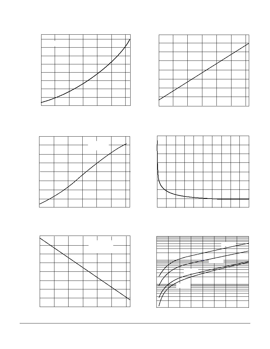
Typical Performance Characteristics
Figure 1. LED Current for Switch Turn-on vs. Temperature
Figure 2. ON-Resistance vs. Temperature
Figure 3. Current Limit vs. Temperature
Ambient Temperature (
∞C)
100
≠60
80
60
40
≠40
≠40
20
≠20
0
≠20
0
20
40
60
80
I
L
= 100 mA
LED Forward Current for Switch
Turn-on (%), Normalized to 25
∞
C
≠40
0
10
20
30
40
≠10
≠40
≠20
≠30
≠20
0
20
40
60
Ambient Temperature (
∞C)
80
I
F
= 5.0 mA
I
L
= 50 mA
Change in R
ON
(%)
≠40
40
10
30
20
0
≠20
≠10
≠40
≠30
≠20
0
20
40
60
Ambient Temperature (
∞C)
80
I
F
= 5.0 mA
t = 5.0 ms
V
L
=
SEE ELEC. CHAR
.
Change in Current Limit (%)
Normalized to 25
∞
C
Figure 4. Switch Breakdown Voltage vs. Temperature
Figure 5. Switch Capacitance vs. Applied Voltage
Figure 6. Leakage Current vs. Applied Voltage
≠40
≠20
0
20
40
60
80
Ambient Temperature (
∞C)
8
0
4
2
6
≠2
≠6
≠8
≠4
Change in Breakdown Voltage (%)
Normalized to 25
∞
C
0
20
40
Applied Voltage (V)
80
50
70
60
40
20
0
10
60
30
100
80
Capacitance (pF)
0
50
100
Load Voltage (V)
150
200
250
300
350
400
0.1
1.0
10
100
Leakage (pA)
T=25
∞C
T=50
∞C
T=70
∞C
T=85
∞C

Document Number: 83830
www.vishay.com
Revision 17-August-01
3≠142
Figure 7. Leakage Current vs. Applied Voltage
Figure 8. Turn-off Time vs. Temperature
Figure 9. Turn-on Time vs. LED Current
0
50
100
Load Voltage (V)
150
200
250
300
350
400
1
10
100
1000
10000
Leakage (pA)
≠80
≠60
≠40
≠20
0
20
40
60
80
Change in T
off (%)
Normalized to 25
∞
C
≠40
≠20
0
20
40
60
Ambient Temperature (
∞C)
80
I
F
=10 mA
I
F
=8.0 mA
I
F
=6.0 mA
I
F
=5.0 mA
I
F
=4.0 mA
I
F
=3.0 mA
I
F
=2.0 mA
0
1
2
3
4
5
6
7
T
on (ms)
0
5
10
15
20
25
30
35
40
45
LED Forward Current (mA)
50
T=85
∞C
T=25
∞C
T=≠45
∞C