
LH1550AT1/ AAB1/ AAB1TR
Document Number 83841
Rev. 1.5, 26-Oct-04
Vishay Semiconductors
www.vishay.com
1
4
6
5
S'
S
NC
1
2
3
S
S'
i179003
DIP
SMD
Pb
Pb-free
e3
1 Form A High-Voltage Solid State Relay
Features
∑ Current Limit Protection
∑ Isolation Test Voltage 5300 V
RMS
∑ Typical R
ON
28
∑ Load Voltage 350 V
∑ Load Current 120 mA
∑ High Surge Capability
∑ Clean Bounce Free Switching
∑ Low Power Consumption
∑ High Reliability Monolithic Detector
∑ SMD Lead Available on Tape and Reel
∑ Lead-free component
∑ Component in accordance to RoHS 2002/95/EC
and WEEE 2002/96/EC
Agency Approvals
∑ UL1577, File No. E52744 System Code H or J,
Double Protection
∑ BABT/BSI Certified
Applications
General Telecom Switching
- On/off Hook Control
- Ring Delay
- Dial Pulse
- Ground Start
- Ground Fault Protection
Instrumentation
Industrial Controls
Description
The LH1550 is robust, ideal for telecom and ground
fault applications. It is a SPST normally open switch
(1 Form A) that replaces electromechanical relays in
many applications. It is similar to the LH1540, but has
a characteristically higher On resistance. It is con-
structed using a GaAIAs LED for actuation control
and an integrated monolithic die for the switch output.
The die, fabricated in a high-voltage dielectrically iso-
lated technology, is comprised of a photodiode array,
switch control circuitry and MOSFET switches. In
addition, it employs current-limiting circuitry which
meets FCC 68.302 and other regulatory voltage
surge requirements when overvoltage protection is
provided.
Order Information
Part
Remarks
LH1550AT1
Thru Hole, DIP-6
LH1550AAB1
SMD-6
LH1550AAB1TR
Tape and Reel, SMD-6

www.vishay.com
2
Document Number 83841
Rev. 1.5, 26-Oct-04
LH1550AT1/ AAB1/ AAB1TR
Vishay Semiconductors
Absolute Maximum Ratings, T
amb
= 25 ∞C
Stresses in excess of the absolute Maximum Ratings can cause permanent damage to the device. Functional operation of the device is
not implied at these or any other conditions in excess of those given in the operational sections of this document. Exposure to absolute
Maximum Ratings for extended periods of time can adversely affect reliability.
SSR
1)
Refer to Current Limit Performance Application Note 58 for a discussion on relay operation during transient currents.
Electrical Characteristics, T
amb
= 25 ∞C
Minimum and maximum values are testing requirements. Typical values are characteristics of the device and are the result of engineering
evaluations. Typical values are for information only and are not part of the testing requirements.
Input
Output
Parameter
Test condition
Symbol
Value
Unit
LED continuous forward current
I
F
50
mA
LED reverse voltage
I
R
10 µA
V
R
8.0
V
DC or peak AC load voltage
I
L
50 µA
V
L
350
V
Continuous DC load current -
bidirectional operation
I
L
100
mA
Peak load current (single shot)
t = 100 ms
I
P
1)
Ambient temperature range
T
amb
- 40 to + 85
∞C
Storage temperature range
T
stg
- 40 to + 150
∞C
Pin soldering temperature
t = 10 s max
T
sld
260
∞C
Input/output isolation voltage
V
RMS
t = 1.0 s, I
ISO
= 10
µA
V
ISO
5300
V
RMS
Output power dissipation
(continuous)
P
diss
550
mW
Parameter
Test condition
Symbol
Min
Typ.
Max
Unit
LED forward current, switch
turn-on
I
L
= 100 mA, t = 10 ms
I
Fon
1.1
2.0
mA
LED forward current, switch
turn-off
V
L
= ± 350 V
I
Foff
0.001
1.0
-
mA
LED forward voltage
I
F
= 10 mA
V
F
1.15
1.25
1.45
V
Parameter
Test condition
Symbol
Min
Typ.
Max
Unit
ON-resistance, ac:
Pin 4 (±) to 6 (±)
I
F
= 5.0 mA, I
L
= 50 mA
R
ON
28
50
OFF-resistance
I
F
= 0 mA, V
L
= ± 100 V
R
OFF
0.5
300
-
G
Current limit ac/dc
I
F
= 5.0 mA, t = 5.0 ms,
V
L
= 6.0 V
I
LMT
170
210
250
mA
Off-state leakage current
I
F
= 0 mA, V
L
= ± 100 V
I
O
0.35
200
nA
I
F
= 0 mA, V
L
= ± 350 V
I
O
0.09
1.0
µA
Output capacitance Pin 4 to 6
I
F
= 0 mA, V
L
= 1.0 V
C
O
18
pF
I
F
= 0 mA, V
L
= 50 V
C
O
7
pF
Switch Offset
I
F
= 5.0 mA
V
OS
0.3
µV

LH1550AT1/ AAB1/ AAB1TR
Document Number 83841
Rev. 1.5, 26-Oct-04
Vishay Semiconductors
www.vishay.com
3
Transfer
Typical Characteristics (Tamb = 25
∞C unless otherwise specified)
Parameter
Test condition
Symbol
Min
Typ.
Max
Unit
Capacitance (input-output)
V
ISO
= 1.0 V
C
IO
0.7
pF
Turn-on time
I
F
= 5.0 mA, I
L
= 50 mA
t
on
1.1
3.0
ms
Turn-off time
I
F
= 5.0 mA, I
L
= 50 mA
t
off
0.7
3.0
ms
Figure 1. Recommended Operating Conditions
Figure 2. LED Voltage vs. Temperature
i1550at_00
80
60
40
20
≠40
≠20
0
20
40
60
80
Ambient Temperature (∞C)
0
100
= 2.0 mA
Load
Current
(mA)
I
Fon
= 3.0 mA
I
Fon
I
Fon
=
4.5 to 20 mA
i1550at_01
AMBIENT TEMPERATURE, T
A
(∞C)
LED
F
ORWAD
V
OLTAGE
(V)
≠40
≠20
1.6
1.5
1.4
1.3
1.2
1.1
1.0
I
F
= 20 mA
I
F
= 1 mA
I
F
= 2 mA
I
F
= 5 mA
I
F
= 10 mA
I
F
= 50 mA
0
20
40
60
80
Figure 3. Current Limit vs. Temperature
Figure 4. Turn-on Time vs. Temperature
i1550at_02
40
30
20
10
0
≠10
≠20
≠30
≠40
CHANGE
IN
CURRENT
LIMIT
(
%)
NORMALIZED
TO
25∞
C
I
F
= 5 mA, t = 5 ms
AMBIENT TEMPERATURE, T
A
(∞C)
≠40
≠20
0
20
40
60
80
i1550at_03
AMBIENT TEMPERATURE, T
A
(∞C)
≠40
≠20
0
20
40
60
80
70
60
50
40
30
20
10
0
≠10
≠20
≠30
≠40
CHANGE
IN
TURN-ON
TIME
(%)
NORMALIZED
T
O
25∞
C
I
F
= 5 mA
I
F
= 50 mA

www.vishay.com
4
Document Number 83841
Rev. 1.5, 26-Oct-04
LH1550AT1/ AAB1/ AAB1TR
Vishay Semiconductors
Figure 5. LED Current for Switch Turn-on/off vs. Temperature
Figure 6. ON-Resistance vs. Temperature
Figure 7. Turn-off Time vs. Temperature
i1545at_04
300
200
100
0
≠100
I
F
= 50 mA
LED
F
ORWAD
C
URRENT
FOR
S
WITCH
TURN-0N/OFF
(
%)
NORMALIZED
T
O
25∞
C
AMBIENT TEMPERATURE, T
A
(∞C)
≠40
≠20
0
20
40
60
80
i1550at_05
CHANGE
IN
ON-RESISTANCE
(
%)
NORMALIZED
TO
25∞
C
60
50
40
30
20
10
0
≠10
≠20
≠30
≠40
I
L
= 5 mA
AMBIENT TEMPERATURE, T
A
(∞C)
≠40
≠20
0
20
40
60
80
i1550at_06
80
75
50
25
0
≠25
≠50
CHANGE
I
N
T
URN-OFF
T
IME
(
%)
NORMALIZED
T
O
25∞
C
I
F
= 5 MA
I
L
= 50 MA
AMBIENT TEMPERATURE, T
A
(∞C)
≠40
≠20
0
20
40
60
80
LH1550AT1/ AAB1/ AAB1TR
Document Number 83841
Rev. 1.5, 26-Oct-04
Vishay Semiconductors
www.vishay.com
5
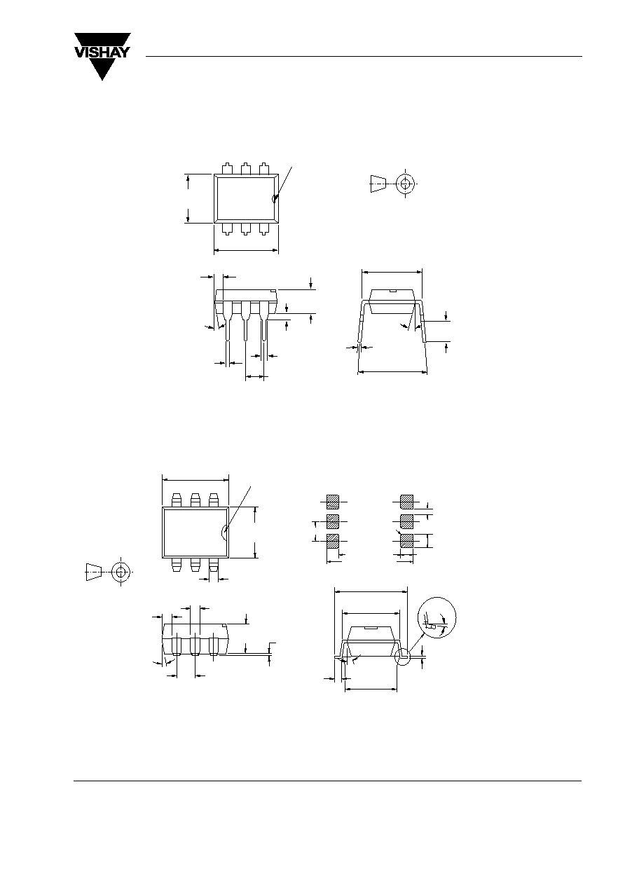
Package Dimensions in Inches (mm)
Package Dimensions in Inches (mm)
.014 (.35)
.010 (.25)
.150 (3.81)
.110 (2.79)
.150 (3.81)
.130 (3.30)
.020 (.051) Min.
.300 (7.62)
Typ.
.035 (0.90)
.031 (0.80)
.100 (2.54) Typ.
.039
(1.00)
Min.
.022 (0.55)
.018 (0.45)
.256 (6.50)
.248 (6.30)
.343 (8.70)
.335 (8.50)
Pin One ID.
6
5
4
1
2
3
18
∞ Typ.
.347 (8.82)
.300 (7.62)
4
∞ Typ.
DIP
ISO Method A
i178001
.343 (8.71)
.335 (8.51)
.256 (6.50)
.248 (6.30)
Pin one I.D.
.039
(0.99)
min.
.150 (3.81)
.130 (3.30)
.100 (2.54)
.052 (1.33)
.048 (1.22)
4
∞
.040 (1.016)
.020 (0.508)
.0098 (.25)
.0040 (.10)
.012 (0.31)
.008 (0.20)
.300 (7.62)
.395 (10.03)
.375 (9.63)
3
∞ to 7∞
18
∞
min.
.315 (8.00)
typ.
.050 (1.27) typ.
SMD
ISO Method A
i178002
.100 (2.54)
R .010 (.25)
.070 (1.78)
.030 (.76)
.060 (1.52)
.315 (8.00) min
.435 (11.05)