Si91841/3
Vishay Siliconix
Document Number: 71447
S-40592--Rev. C, 29-Mar-04
www.vishay.com
1
150-mA Ultra Low-Noise LDO Regulator
With Discharge Option
FEATURES
D Ultra Low Dropout--130 mV at 150-mA Load
D Ultra Low Noise--30 mV
(rms)
(10-Hz to 100-kHz
Bandwidth)
D Shutdown Control
D 110-mA Ground Current at 150-mA Load
D 1.5% Guaranteed Output Voltage Accuracy
D 300-mA Peak Output Current Capability
D Uses Low ESR Ceramic Capacitors
D Fast Start-Up (50 ms)
D Fast Line and Load Transient Response (v 30 ms)
D 1-mA Maximum Shutdown Current
D Output Current Limit
D Reverse Battery Protection
D Built-in Short Circuit and Thermal Protection
D Si91841: Output, Auto-Discharge In Shutdown Mode
D Si91843: Output, No-Discharge In Shutdown Mode
D Fixed 1.8, 2.0, 2.2, 2.5, 2.6, 2.7, 2.8, 2.85, 2.9, 3.0, 3.3,
3.5, 3.6, 5.0-V Output Voltage Options
D Thin SOT23-5 Package
APPLICATIONS
D Cellular Phones, Wireless Handsets
D Noise-Sensitive Electronic Systems, Laptop and
Palmtop Computers
D PDAs
D Pagers
D Digital Cameras
D MP3 Player
D Wireless Modem
DESCRIPTION
The Si91841/3 is a 150-mA CMOS LDO (low dropout) voltage
regulator. It is the perfect choice for low voltage, low power
applications. An ultra low ground current makes this part
attractive for battery operated power systems. The Si91841/3
also offers ultra low dropout voltage to prolong battery life in
portable electronics. Systems requiring a quiet voltage
source, such as RF applications, will benefit from the
Si91841/3's ultra low output noise. An external noise bypass
capacitor connected to the device's BP pin can further reduce
the noise level. The Si91841/3 is designed to maintain
regulation while delivering 300-mA peak current, making it
ideal for systems that have a high surge current upon turn-on.
For better transient response and regulation, an active
pull-down circuit is built into the Si91841/3 to clamp the output
voltage when it rises beyond normal regulation. The Si91841
automatically discharges the output voltage by connecting the
output to ground through a 100-W n-channel MOSFET when
the device is put in shutdown mode.
The Si91841/3 features reverse battery protection to limit
reverse current flow to approximately 1-mA in the event
reversed battery is applied at the input, thus preventing
damage to the IC.
The Si91841/3 is available in both standard and lead (Pb)-free
packages.
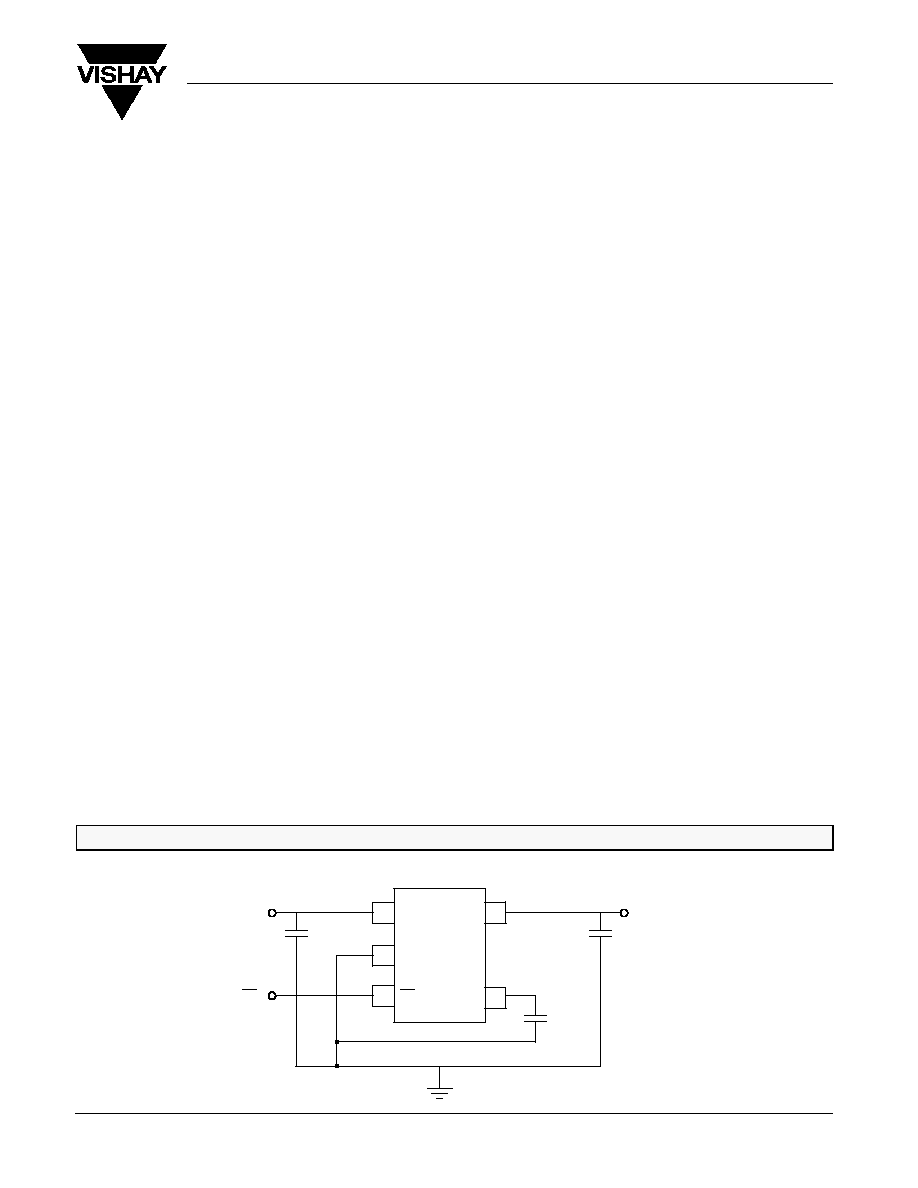
TYPICAL APPLICATION CIRCUIT
3
2
Si91841/3
1
4
5
V
IN
GND
SD
V
OUT
V
IN
SD
V
OUT
1 mF
1 mF
BP
10 nF
Thin SOT-23, 5-Lead
Si91841/3
Vishay Siliconix
www.vishay.com
2
Document Number: 71447
S-40592--Rev. C, 29-Mar-04
ABSOLUTE MAXIMUM RATINGS
Absolute Maximum Ratings
Input Voltage, V
IN
to GND
-6.0 to 6.5 V
. . . . . . . . . . . . . . . . . . . . . . . . . . . . . . . . . . . . . .
V
SD
(See Detailed Description)
-0.3 V to V
IN
. . . . . . . . . . . . . . . . . . . . . . . . . . . . . . . . .
Output Current, I
OUT
Short Circuit Protected
. . . . . . . . . . . . . . . . . . . . . . . . . . . . . . . . .
Output Voltage, V
OUT
-
0.3 V to V
IN
+ 0.3 V
. . . . . . . . . . . . . . . . . . . . . . . . . . . . . . . . . . .
Package Power Dissipation, (P
d
)
b
440 mW
. . . . . . . . . . . . . . . . . . . . . . . . . . .
Package Thermal Resistance, (q
JA
)
a
180_C/W
. . . . . . . . . . . . . . . . . . . . . . . . .
Maximum Junction Temperature, T
J(max)
150_C
. . . . . . . . . . . . . . . . . . . . . . .
Storage Temperature, T
STG
-65_C to 150_C
. . . . . . . . . . . . . . . . . . . . . . . . . .
Notes
a.
Device mounted with all leads soldered or welded to PC board.
b.
Derate 5.5 mW/_C above T
A
= 70_C
Stresses beyond those listed under "Absolute Maximum Ratings" may cause permanent damage to the device. These are stress ratings only, and functional operation
of the device at these or any other conditions beyond those indicated in the operational sections of the specifications is not implied. Exposure to absolute maximum rating
conditions for extended periods may affect device reliability.
RECOMMENDED OPERATING RANGE
Input Voltage, V
IN
2 V to 6 V
. . . . . . . . . . . . . . . . . . . . . . . . . . . . . . . . . . . . . . . .
Input Voltage, V
SD
0 V to V
IN
. . . . . . . . . . . . . . . . . . . . . . . . . . . . . . . . . . . . . . .
Operating Ambient Temperature, T
A
-40_C to 85_C
. . . . . . . . . . . . . . . . . . . .
C
IN
= C
OUT
= 1
m
F (ceramic), C
BP
= 0.01
m
F (ceramic)
Maximum ESR of C
OUT
: 0.4
W
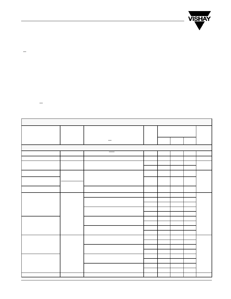
SPECIFICATIONS
Test Conditions Unless Specified
T
A
= 25_C, V
IN
= V
OUT(nom)
+ 1 V
C
C
Limits
-40 to 85_C
Parameter
Symbol
(
)
I
OUT
= 1 mA, C
IN
= 1 mF, C
OUT
= 1.0 mF
V
SD
= 1.5 V
Temp
a
Min
b
Typ
c
Max
b
Unit
Start-Up BP Current
I
OUT
ON/OFF = High
Room
1
mA
Input Voltage Range
V
IN
Full
2
6
V
Output Voltage Accuracy
V
OUT
1 mA v I
OUT
v 150 mA
Room
-1.5
1
1.5
%
Output Voltage Accuracy
V
OUT
1 mA v I
OUT
v 150 mA
Full
-2.5
1
2.5
%
Line Regulation (V
OUT
v 3 V)
Full
-0.06
0.18
Line Regulation
(3.0 V < V
OUT
v3.6 V)
DV
OUT
100
DV
IN
V
OUT(nom)
From V
IN
= V
OUT(nom)
+ 1 V to V
OUT(nom)
+ 2 V
Full
0
0.3
%/V
Line Regulation (5-V Version)
IN
OUT(nom)
From V
IN
= 5.5 V to 6 V
Full
0
0.4
I
OUT
= 1 mA
Room
1
D
t V lt
d g
I
OUT
= 50 mA
Room
45
80
Dropout Voltage
d, g
(V
OUT(nom)
w 2.6 V)
I
OUT
= 50 mA
Full
50
90
(V
OUT(nom)
w 2.6 V)
I
OUT
= 150 mA
Room
130
180
V
IN
- V
OUT
I
OUT
= 150 mA
Full
220
mV
IN
OUT
I
OUT
= 50 mA
Room
65
100
Dropout Voltage
d, g
(V
OUT(
)
t 2 6 V V
IN
w
I
OUT
= 50 mA
Full
120
(V
OUT(nom)
t 2.6 V, V
IN
w
2 V)
I
OUT
= 150 mA
Room
190
250
2 V)
I
OUT
= 150 mA
Full
300
I
OUT
= 0 mA
Room
100
150
Ground Pin Current
e, g
I
OUT
= 0 mA
Full
180
Ground Pin Current
e, g
(V
OUT(nom)
v 3 V)
I
OUT
= 150 mA
Room
110
200
I
GND
I
OUT
= 150 mA
Full
230
mA
I
GND
I
OUT
= 0 mA
Room
110
170
mA
Ground Pin Current
e
I
OUT
= 0 mA
Full
200
Ground Pin Current
e
(V
OUT(nom)
u 3 V)
I
OUT
= 150 mA
Room
120
200
I
OUT
= 150 mA
Full
230
Peak Output current
I
O(peak)
V
OUT
w 0.95 x V
OUT(nom)
. t
PW
= 2 ms
Full
300
mA
Si91841/3
Vishay Siliconix
Document Number: 71447
S-40592--Rev. C, 29-Mar-04
www.vishay.com
3
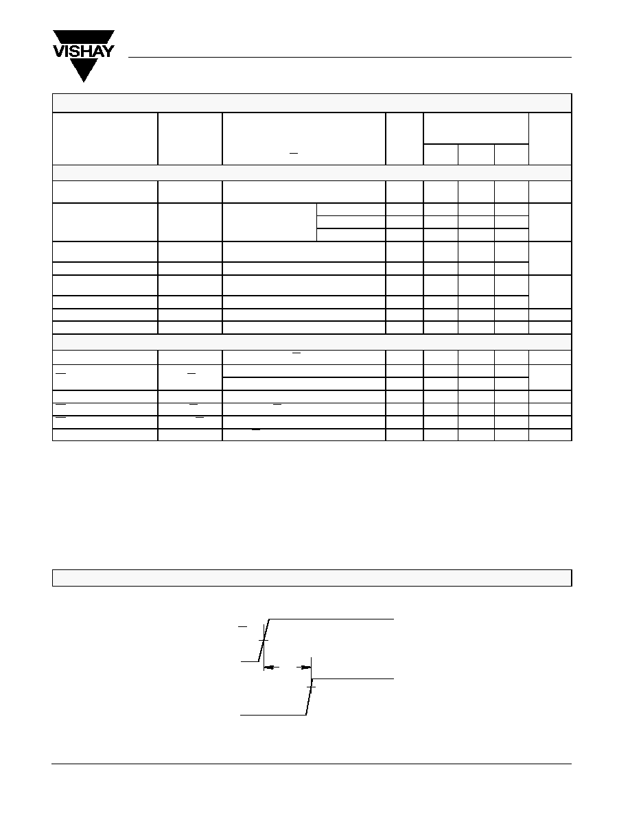
SPECIFICATIONS
Limits
-40 to 85_C
Temp
a
Test Conditions Unless Specified
T
A
= 25_C, V
IN
= V
OUT(nom)
+ 1 V
I
OUT
= 1 mA, C
IN
= 1 mF, C
OUT
= 1.0 mF
V
SD
= 1.5 V
Parameter
Unit
Max
b
Typ
c
Min
b
Temp
a
Test Conditions Unless Specified
T
A
= 25_C, V
IN
= V
OUT(nom)
+ 1 V
I
OUT
= 1 mA, C
IN
= 1 mF, C
OUT
= 1.0 mF
V
SD
= 1.5 V
Symbol
Output Noise Voltage
e
N
V
NOM
= 2.6 V, BW = 10 Hz to 100 kHz,
0 mA t I
OUT
t 150 mA, C
NOISE
= 0.01 mF
Room
30
mV(rms)
f = 1 kHz
Room
60
Ripple Rejection
DV
OUT
/DV
IN
I
OUT
= 150 mA
f = 10 kHz
Room
40
dB
pp
j
OUT
IN
OUT
f = 100 kHz
Room
30
Dynamic Line Regulation
DV
O(line)
V
IN
: V
OUT(nom)
+ 1 V to V
OUT(nom)
+ 2 V
t
r
/t
f
= 2 ms, I
OUT
= 150 mA
Room
20
mV
Dynamic Load Regulation
DV
O(load)
I
OUT
: 1 mA to 150 mA, t
r
/t
f
= 2 ms
Room
20
mV
Thermal Shutdown Junction
Temperature
T
J(S/D)
Room
150
_C
Thermal Hysteresis
T
HYST
Room
20
C
Reverse current
I
R
V
IN
= -6.0 V
Room
1
mA
Short Circuit Current
I
SC
V
OUT
= 0 V
Room
700
mA
Shutdown
Shutdown Supply Current
I
CC(off)
V
SD
= 0 V
Room
0.1
1
mA
SD Pin Input Voltage
V
SD
High = Regulator ON (Rising)
Full
1.5
V
IN
V
SD Pin Input Voltage
V
SD
Low = Regulator OFF (Falling)
Full
0.4
V
Auto Discharge Resistance
R_DIS
Si91841 Only
Room
100
W
SD Pin Input Current
f
I
IN(SD)
V
SD
= 1.5 V, V
IN
= 6 V
Room
0.7
mA
SD Hysteresis
V
HYST(SD)
Full
150
mV
V
OUT
Turn-On Time
t
ON
V
SD
(See Figure 1), I
LOAD
= 100 nA
50
mS
Notes
a.
Room = 25_C, Full = -40 to 85_C.
b.
The algebraic convention whereby the most negative value is a minimum and the most positive a maximum.
c.
Typical values are for DESIGN AID ONLY, not guaranteed nor subject to production testing. Typical values for dropout voltage at V
OUT
w 2 V are measured at
V
OUT
= 3.3 V, while typical values for dropout voltage at V
OUT
< 2 V are measured at V
OUT
= 1.8 V.
d.
Dropout voltage is defined as the input to output differential voltage at which the output voltage drops 2% below the output voltage measured with a 1-V
differential, provided that V
IN
does not not drop below 2.0 V.
e.
Ground current is specified for normal operation as well as "drop-out" operation.
f.
The device's shutdown pin includes a typical 2-MW internal pull-down resistor connected to ground.
g.
V
OUT(nom)
is V
OUT
when measured with a 1-V differential to V
IN.
TIMING WAVEFORMS
FIGURE 1. Timing Diagram for Power-Up
V
SD
0.95 V
NOM
V
OUT
V
NOM
t
ON
0 V
V
IN
t
r
v 1 ms
SD
3
2
Thin SOT-23, 5-Lead
1
4
5
V
IN
GND
V
OUT
BP
Si91841/3
Vishay Siliconix
www.vishay.com
4
Document Number: 71447
S-40592--Rev. C, 29-Mar-04
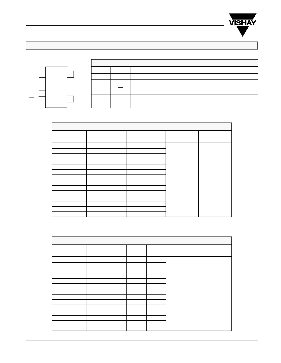
PIN CONFIGURATION
PIN DESCRIPTION
Pin No.
Name
Function
1
V
IN
Input supply pin. Bypass this pin with a 1-mF ceramic or tantalum capacitor to ground
2
GND
Ground pin. For better thermal capability, directly connected to large ground plane
3
SD
By applying less than 0.4 V to this pin, the device will be turned off. Connect this pin to
V
IN
if unused
4
BP
Noise bypass pin. For low noise applications, a 0.01 mF ceramic capacitor should be
connected from this pin to ground.
5
V
OUT
Output voltage. Connect C
OUT
between this pin and ground.
ORDERING INFORMATION Si91841
Part Number
Lead (Pb)-Free
Part Number
Marking Voltage
Temperature
Range
Package
Si91841DT-18-T1
Si91841DT-18-T1--E3
B4LL
1.8
Si91841DT-20-T1
Si91841DT-20-T1--E3
B5LL
2.0
Si91841DT-22-T1
Si91841DT-22-T1--E3
B6LL
2.2
Si91841DT-25-T1
Si91841DT-25-T1--E3
B7LL
2.5
Si91841DT-26-T1
Si91841DT-26-T1--E3
B8LL
2.6
Si91841DT-27-T1
Si91841DT-27-T1--E3
B9LL
2.7
Si91841DT-28-T1
Si91841DT-28-T1--E3
B0LL
2.8
-40 to 85_C
Thin SOT23-5
Si91841DT-285-T1
Si91841DT-285--E3
C1LL
2.85
-40 to 85_C
Thin SOT23-5
Si91841DT-29-T1
Si91841DT-29-T1--E3
C2LL
2.9
Si91841DT-30-T1
Si91841DT-30-T1--E3
C3LL
3.0
Si91841DT-33-T1
Si91841DT-33-T1--E3
C4LL
3.3
Si91841DT-35-T1
Si91841DT-35-T1--E3
C5LL
3.5
Si91841DT-36-T1
Si91841DT-36-T1--E3
C6LL
3.6
Si91841DT-50-T1
Si91841DT-50-T1--E3
C7LL
5.0
Note: LL = Lot Code
ORDERING INFORMATION Si91843
Part Number
Lead (Pb)-Free
Part Number
Marking Voltage
Temperature
Range
Package
Si91843DT-18-T1
Si91843DT-18-T1--E3
E2LL
1.8
Si91843DT-20-T1
Si91843DT-20-T1--E3
E3LL
2.0
Si91843DT-22-T1
Si91843DT-22-T1--E3
E4LL
2.2
Si91843DT-25-T1
Si91843DT-25-T1--E3
E5LL
2.5
Si91843DT-26-T1
Si91843DT-26-T1--E3
E6LL
2.6
Si91843DT-27-T1
Si91843DT-27-T1--E3
E7LL
2.7
Si91843DT-28-T1
Si91843DT-28-T1--E3
E8LL
2.8
-40 to 85_C
Thin SOT23-5
Si91843DT-285-T1
Si91843DT-285--E3
E9LL
2.85
-40 to 85_C
Thin SOT23-5
Si91843DT-29-T1
Si91843DT-29-T1--E3
E0LL
2.9
Si91843DT-30-T1
Si91843DT-30-T1--E3
F1LL
3.0
Si91843DT-33-T1
Si91843DT-33-T1--E3
F2LL
3.3
Si91843DT-35-T1
Si91843DT-35-T1--E3
F3LL
3.5
Si91843DT-36-T1
Si91843DT-36-T1--E3
F4LL
3.6
Si91843DT-50-T1
Si91843DT-50-T1--E3
F5LL
5.0
Note: LL = Lot Code
Si91841/3
Vishay Siliconix
Document Number: 71447
S-40592--Rev. C, 29-Mar-04
www.vishay.com
5
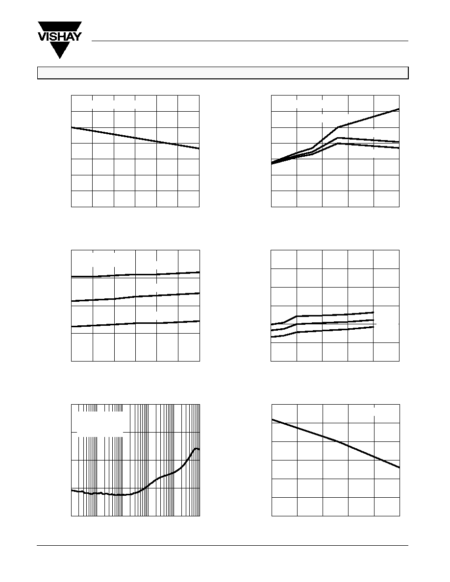
TYPICAL CHARACTERISTICS (INTERNALLY REGULATED, 25_C UNLESS NOTED)
-1.0
-0.8
-0.6
-0.4
-0.2
-0.0
0.2
0.4
-40
-15
10
35
60
85
Normalized V
OUT
vs. Temperature
Ambient Temperature (_C)
(%)
V
OUT
0
50
100
150
200
250
300
2
3
4
5
6
7
No Load GND Pin Current vs. Input Voltage
(
I
GND
m
A)
Input Voltage (V)
I
OUT
= 0 mA
I
OUT
= 150 mA
I
OUT
= 75 mA
-40_C
85_C
50
75
100
125
150
0
25
50
75
100
125
150
GND Current vs. Load Current
(
I
GND
m
A)
Load Current (mA)
600
625
650
675
700
725
750
-40
-15
10
35
60
85
Output Short Circuit Current vs. Temperature
25_C
(mA)
I
SC
AmbientTemperature (_C)
25_C
-80
-60
-40
-20
0
10
100
1000
10000
100000
1000000
Power Supply Rejection
Frequency (Hz)
Gain (dB)
C
IN
= 1 mF
C
OUT
= 1 mF
I
LOAD
= 150 mA
V
OUT
= 3.0 V
-0.75
-0.60
-0.45
-0.30
-0.15
0.00
0.15
0.30
0
25
50
75
100
125
150
Normalized Output Voltage vs. Load Current
Output V
oltage (%)
Load Current (mA)
V
OUT
= 2.6 V
V
IN
= V
OUT(nom)
+ 1 V
V
OUT
= 3.0 V
V
IN
= 4.0 V
V
IN
= V
OUT(nom)
+ 1 V
-40_C
85_C