 | –≠–ª–µ–∫—Ç—Ä–æ–Ω–Ω—ã–π –∫–æ–º–ø–æ–Ω–µ–Ω—Ç: SI9928DY | –°–∫–∞—á–∞—Ç—å:  PDF PDF  ZIP ZIP |
Si9928DY
Vishay Siliconix
Document Number: 70143
S-00652--Rev. G, 27-Mar-00
www.vishay.com
S
FaxBack 408-970-5600
1
Complimentary 20-V (D-S) MOSFET
PRODUCT SUMMARY
V
DS
(V)
r
DS(on)
(
W
)
I
D
(A)
N Ch
l
20
0.05 @ V
GS
= 4.5 V
"
5.0
N-Channel
20
0.06 @ V
GS
= 3.0 V
"
4.2
0.08 @ V
GS
= 2.7 V
"
3.6
P Ch
l
20
0.11 @ V
GS
= ≠4.5 V
"
3.4
P-Channel
≠20
0.15 @ V
GS
= ≠3.0 V
"
2.9
0.19 @ V
GS
= ≠2.7 V
"
2.6
S
1
D
1
G
1
D
1
S
2
D
2
G
2
D
2
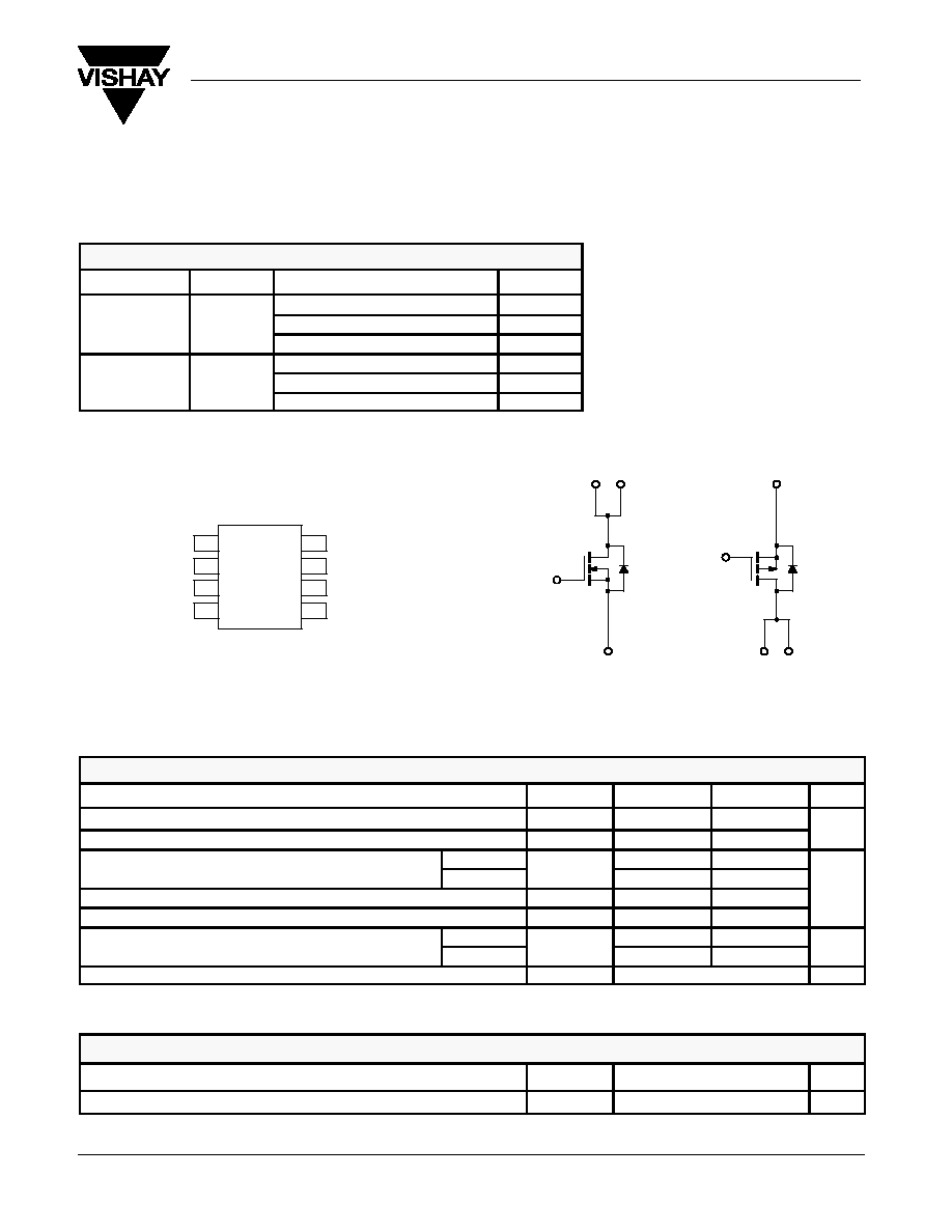
SO-8
5
6
7
8
Top View
2
3
4
1
N-Channel MOSFET
D
1
D
1
G
1
S
1
S
2
G
2
D
2
D
2
P-Channel MOSFET
ABSOLUTE MAXIMUM RATINGS (T
A
= 25_C UNLESS OTHERWISE NOTED)
Parameter
Symbol
N-Channel
P-Channel
Unit
Drain-Source Voltage
V
DS
20
≠20
V
Gate-Source Voltage
V
GS
"
12
"
12
V
Continuous Drain Current
(T
J
= 150
_
C)
a
T
A
= 25
_
C
I
D
"
5.0
"
3.4
A
Continuous Drain Current
(T
J
= 150
_
C)
a
T
A
= 70
_
C
I
D
"
4.0
"
2.8
A
Pulsed Drain Current
I
DM
"
10
"
10
A
Continuous Source Current (Diode Conduction)
a
I
S
2.0
≠2.0
Maximum Power Dissipation
a
T
A
= 25
_
C
P
D
2.0
2.0
W
Maximum Power Dissipation
a
T
A
= 70
_
C
P
D
1.3
1.3
W
Operating Junction and Storage Temperature Range
T
J
, T
stg
≠55 to 150
_
C
THERMAL RESISTANCE RATINGS
Parameter
Symbol
N- or P-Channel
Unit
Maximum Junction-to-Ambient
a
R
thJA
62.5
_
C/W
Notes
a.
Surface Mounted on FR4 Board, t
v
10 sec.
Si9928DY
Vishay Siliconix
www.vishay.com
S
FaxBack 408-970-5600
2
Document Number: 70143
S-00652--Rev. G, 27-Mar-00
SPECIFICATIONS (T
J
= 25_C UNLESS OTHERWISE NOTED)
Parameter
Symbol
Test Condition
Min
Typ
a
Max
Unit
Static
Gate Threshold Voltage
V
GS(th)
V
DS
= V
GS
, I
D
= 250
m
A
N-Ch
0.8
1.2
V
Gate Threshold Voltage
V
GS(th)
V
DS
= V
GS
, I
D
= ≠250
m
A
P-Ch
≠0.8
≠1.1
V
Gate-Body Leakage
I
GSS
V
DS
= 0 V, V
GS
=
"
12 V
N-Ch
"
100
nA
Gate-Body Leakage
I
GSS
V
DS
= 0 V, V
GS
=
"
12 V
P-Ch
"
100
nA
Z
G
V l
D i C
I
V
DS
= 16 V, V
GS
= 0 V
N-Ch
1
A
Zero Gate Voltage Drain Current
I
DSS
V
DS
= ≠ 16 V, V
GS
= 0 V
P-Ch
≠1
m
A
Zero Gate Voltage Drain Current
I
DSS
V
DS
= 10 V, V
GS
= 0 V, T
J
= 70
_
C
N-Ch
5
m
A
V
DS
= ≠10 V, V
GS
= 0 V, T
J
= 70
_
C
P-Ch
≠5
On-State Drain Current
b
I
D(on)
V
DS
w
5 V, V
GS
= 4.5 V
N-Ch
10
A
On-State Drain Current
b
I
D(on)
V
DS
v
≠5 V, V
GS
= ≠4.5 V
P-Ch
≠10
A
D i S
O S
R
i
b
V
GS
= 4.5 V, I
D
= 5.0 A
N-Ch
0.041
0.05
W
D i S
O S
R
i
b
V
GS
= ≠4.5 V, I
D
= ≠3.2 A
P-Ch
0.087
0.11
W
Drain-Source On-State Resistance
b
r
DS(on)
V
GS
= 3.0
V, I
D
= 3.9 A
N-Ch
0.052
0.06
W
Drain-Source On-State Resistance
b
r
DS(on)
V
GS
= ≠
3.0
V, I
D
= ≠2.0 A
P-Ch
0.120
0.15
W
V
GS
= 2.7 V, I
D
= 1.0 A
N-Ch
0.060
0.08
V
GS
= ≠2.7 V, I
D
= ≠1.0 A
P-Ch
0.135
0.19
Forward Transconductance
b
g
fs
V
DS
= 10 V, I
D
= 5.0 A
N-Ch
13
S
Forward Transconductance
b
g
fs
V
DS
= ≠9 V, I
D
= ≠3.2 A
P-Ch
8
S
Diode Forward Voltage
b
V
SD
I
S
= 5.0 A, V
GS
= 0 V
N-Ch
0.9
1.2
V
Diode Forward Voltage
b
V
SD
I
S
= ≠2.0 A, V
GS
= 0 V
P-Ch
≠0.9
≠1.2
V
Dynamic
a
Total Gate Charge
Q
g
N Ch
l
N-Ch
10
20
C
Total Gate Charge
Q
g
N-Channel
V
DS
= 6 V V
GS
= 4 5 V I
D
= 5 0 A
P-Ch
8
20
C
Gate-Source Charge
Q
gs
V
DS
= 6 V,
V
GS
= 4.5 V, I
D
= 5.0 A
P-Channel
N-Ch
2.6
nC
Gate-Source Charge
Q
gs
P-Channel
V
DS
= ≠6 V,
V
GS
= ≠4.5 V, I
D
= ≠3.2 A
P-Ch
1.6
nC
Gate-Drain Charge
Q
gd
N-Ch
3.7
Gate-Drain Charge
Q
gd
P-Ch
3.5
Turn-On Delay Time
t
d(on)
N Ch
l
N-Ch
13
30
Turn-On Delay Time
t
d(on)
N-Channel
P-Ch
22
40
Rise Time
t
r
N-Channel
V
DD
= 6 V, R
L
= 6
W
I
D
^
1 A V
GEN
= 4 5 V R
G
= 6
W
N-Ch
9
40
Rise Time
t
r
I
D
^
1 A, V
GEN
= 4.5 V, R
G
= 6
W
P-Channel
P-Ch
43
80
Turn-Off Delay Time
t
d(off)
P-Channel
V
DD
= ≠6 V, R
L
= 6
W
I
D
^
≠1 A V
GEN
= ≠4 5 V R
G
= 6
W
N-Ch
30
60
ns
Turn-Off Delay Time
t
d(off)
I
D
^
≠1 A, V
GEN
= ≠4.5 V, R
G
= 6
W
P-Ch
35
70
ns
Fall Time
t
f
N-Ch
9
30
Fall Time
t
f
P-Ch
20
40
Source-Drain Reverse Recovery Time
t
rr
I
F
= 5.0 A, di/dt = 100 A/
m
s
N-Ch
100
150
Source-Drain Reverse Recovery Time
t
rr
I
F
= ≠2.0 A, di/dt = 100 A/
m
s
P-Ch
75
100
Notes
a.
For design aid only; not subject to production testing.
b.
Pulse test; pulse width
v
300
m
s, duty cycle
v
2%.
Si9928DY
Vishay Siliconix
Document Number: 70143
S-00652--Rev. G, 27-Mar-00
www.vishay.com
S
FaxBack 408-970-5600
3
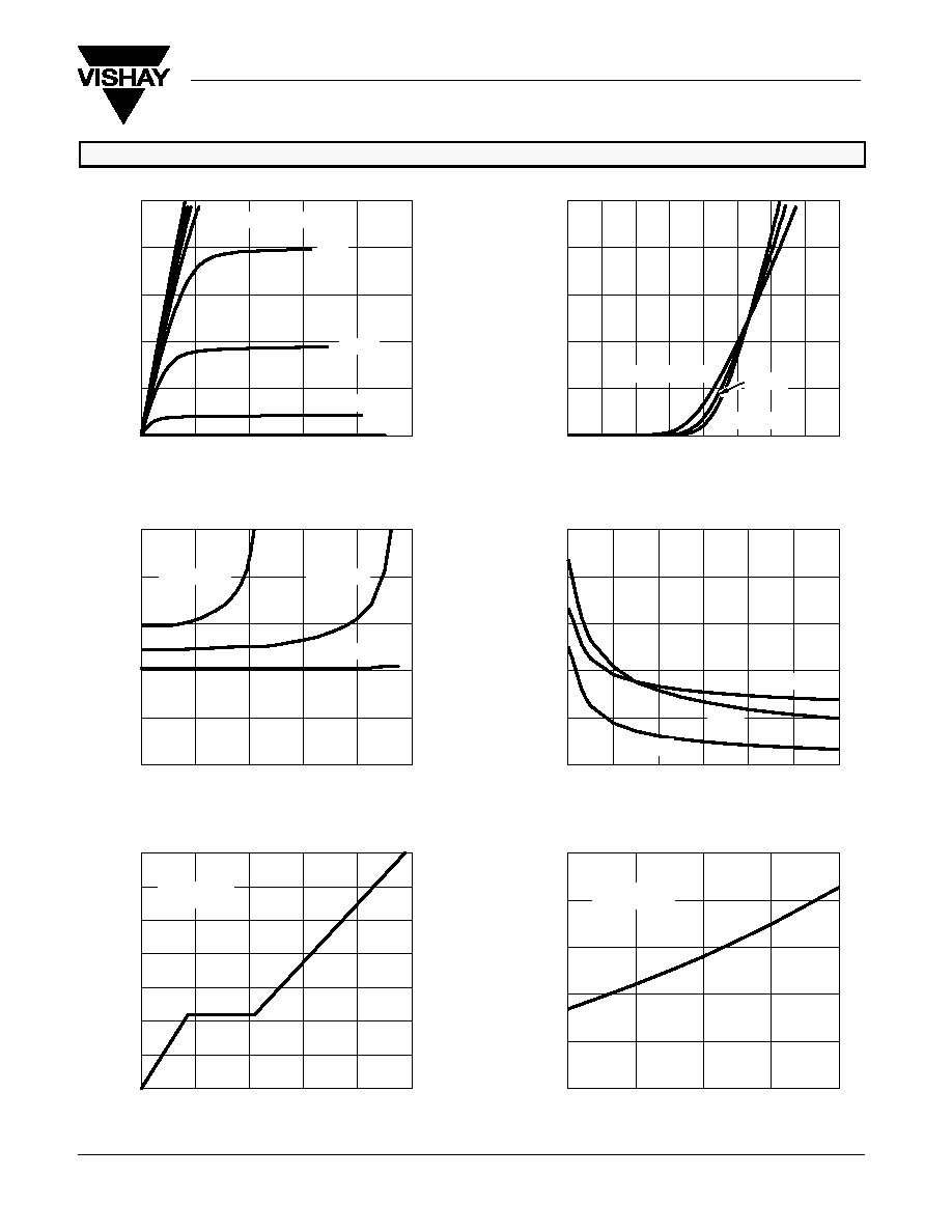
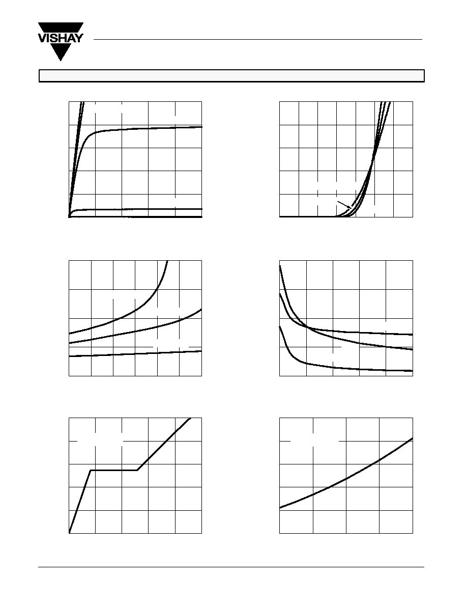
TYPICAL CHARACTERISTICS (25_C UNLESS NOTED)
N CHANNEL
Output Characteristics
Transfer Characteristics
Gate Charge
On-Resistance vs. Drain Current
V
DS
≠ Drain-to-Source Voltage (V)
≠ Drain Current (A)
I
D
V
GS
≠ Gate-to-Source Voltage (V)
≠ Drain Current (A)
I
D
≠ Gate-to-Source V
oltage
(V)
Q
g
≠ Total Gate Charge (nC)
V
DS
≠ Drain-to-Source Voltage (V)
C ≠ Capacitance (pF)
V
GS
≠ On-Resistance (
r
DS(on)
)
I
D
≠ Drain Current (A)
Capacitance
On-Resistance vs. Junction Temperature
T
J
≠ Junction Temperature (
_
C)
(Normalized)
≠ On-Resistance (
r
DS(on)
)
0
4
8
12
16
20
0
1
2
3
4
5
0
1
2
3
4
5
6
7
0
3
6
9
12
15
0
0.4
0.8
1.2
1.6
2.0
≠50
0
50
100
150
0
0.02
0.04
0.06
0.08
0.10
0
4
8
12
16
20
0
400
800
1200
1600
2000
0
2
4
6
8
10
12
0
4
8
12
16
20
0
0.5
1.0
1.5
2.0
2.5
3.0
3.5
4.0
≠55
_
C
V
GS
= 2.7 V
C
rss
C
oss
C
iss
V
GS
= 4.5 V
T
C
= 125
_
C
V
DS
= 6 V
I
D
= 5 A
V
GS
= 4.5 V
I
D
= 5 A
V
GS
= 5.5, 5, 4.5, 4, 3.5 V
2.5 V
3 V
25
_
C
V
GS
= 3 V
2 V
1.5 V
Si9928DY
Vishay Siliconix
www.vishay.com
S
FaxBack 408-970-5600
4
Document Number: 70143
S-00652--Rev. G, 27-Mar-00
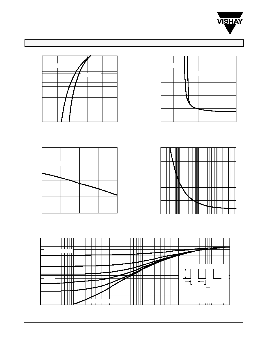
TYPICAL CHARACTERISTICS (25_C UNLESS NOTED)
N CHANNEL
Source-Drain Diode Forward Voltage
On-Resistance vs. Gate-to-Source Voltage
Threshold Voltage
Single Pulse Power
Normalized Thermal Transient Impedance, Junction-to-Ambient
Square Wave Pulse Duration (sec)
Normalized Ef
fective
T
ransient
Thermal Impedance
≠ On-Resistance (
r
DS(on)
)
V
SD
≠ Source-to-Drain Voltage (V)
V
GS
≠ Gate-to-Source Voltage (V)
≠ Source Current (A)
I
S
T
J
≠ Temperature (
_
C)
Time (sec)
Power (W)
≠1
≠0.5
0.0
0.5
1.0
≠50
0
50
100
150
0
1
2
3
4
5
6
T
J
= 150
_
C
T
J
= 25
_
C
2
1
0.1
0.01
I
D
= 5 A
I
D
= 250
µ
A
0
0.4
10
0.8
1.2
1.6
2.0
1
10
≠3
10
≠2
1
10
30
10
≠1
10
≠4
1. Duty Cycle, D =
2. Per Unit Base = R
thJA
= 62.5
_
C/W
3. T
JM
≠ T
A
= P
DM
Z
thJA
(t)
t
1
t
2
t
1
t
2
Notes:
4. Surface Mounted
P
DM
0.01
0
0.1
20
25
5
10
15
1
10
100
Duty Cycle = 0.5
0.2
0.1
0.05
0.02
Single Pulse
20
I
D
= 1 A
V
ariance (V)
V
GS(th)
0.200
0.250
0
0.150
0.100
0.050
Si9928DY
Vishay Siliconix
Document Number: 70143
S-00652--Rev. G, 27-Mar-00
www.vishay.com
S
FaxBack 408-970-5600
5
TYPICAL CHARACTERISTICS (25_C UNLESS NOTED)
P CHANNEL
Output Characteristics
Transfer Characteristics
Gate Charge
On-Resistance vs. Drain Current
V
DS
≠ Drain-to-Source Voltage (V)
≠ Drain Current (A)
I
D
V
GS
≠ Gate-to-Source Voltage (V)
≠ Drain Current (A)
I
D
≠ Gate-to-Source V
oltage
(V)
Q
g
≠ Total Gate Charge (nC)
V
DS
≠ Drain-to-Source Voltage (V)
C ≠ Capacitance (pF)
V
GS
≠ On-Resistance (
r
DS(on)
)
I
D
≠ Drain Current (A)
Capacitance
On-Resistance vs. Junction Temperature
T
J
≠ Junction Temperature (
_
C)
(Normalized)
≠ On-Resistance (
r
DS(on)
)
0
2
4
6
8
10
0
2
4
6
8
10
0
1
2
3
4
5
0
2
4
6
8
10
0.6
0.8
1.0
1.2
1.4
1.6
≠50
0
50
100
150
0.05
0.10
0.15
0.20
0.25
0
1
2
3
4
5
6
0
500
1000
1500
2000
0
2
4
6
8
10
0
2
4
6
8
10
0
0.5
1.0
1.5
2.0
2.5
3.0
3.5
≠55
_
C
V
GS
= 2.7 V
C
rss
C
oss
C
iss
V
GS
= 4.5 V
T
C
= 125
_
C
V
DS
= 6 V
I
D
= 3.2 A
V
GS
= 4.5 V
I
D
= 3.2 A
V
GS
= 5, 4 V
2, 1 V
3 V
25
_
C
V
GS
= 3 V