
1
White Electronic Designs Corporation ∑ (602) 437-1520 ∑ www.wedc.com
White Electronic Designs
EDI8L32128V
July 2004
Rev. 6
White Electronic Designs Corp. reserves the right to change products or specifi cations without notice.
DQ0-DQ7
DQ8-DQ15
DQ16-DQ23
DQ24-DQ31
128Kx32
Memory
Array
A0-A16
G#
W#
E0#
E1#
E2#
E3#
17
FEATURES
128Kx32 CMOS High Speed Static RAM
128Kx32 bit CMOS Static
Analog SHARC
TM
External Memory Solution
ADSP-21060L
ADSP-21062L
Random Access Memory Array
Fast Access Times: 12, 15 and 20ns
User Confi gurable Organization
with
Minimal
Additional
Logic
Master Output Enable and Write Control
TTL Compatible Inputs and Outputs
Fully Static, No Clocks
Surface Mount Package
68 Lead PLCC, No. 99 (JEDEC MO-47AE)
Small Footprint, 0.990 Sq. In.
Multiple
Ground
Pins
for
Maximum
Noise
Immunity
Single 3.3V (±5%) Supply Operation
PIN CONFIGURATIONS AND
BLOCK DIAGRAM
PIN NAMES
The EDI8L32128V is a high speed, 3.3V, four megabit
density Static RAM. The device is available with access
times of 12, 15 and 20ns, allowing the device to support
60MH
Z
DSPs with no wait states. The high speed, 3.3V
supply voltage and byte confi gurability make the device
ideal for interfacing with Analog Devices ADSP-21062L or
ADSP-21060L SHARC DSPs.
The device can be confi gured as a 128Kx32 and used to
create a single chip external data memory solution for the
SHARC (fi gure 1). Providing a 51% space savings when
compared to four 128Kx8, 400mil wide plastic SOJs. The
EDI8L32128V has a 10pf load on the data lines vs. 24pf for
four plastic SOJs. Memory upgrades in the same footprint
can be accomplished with the EDI8L32256V (256Kx32) or
the EDI8L32512V (512KX32). This is covered in detail in
the application report "The EDI's x32 MCM-L SRAM Family:
Integrated Memory Solution for the Analog SHARC DSP"
Alternatively the device's chip enables can confi gure it as a
256Kx16. A 256Kx48 program memory array for the SHARC
is created using three devices (fi gure 2). If this memory is
too deep, two 128Kx24's (EDI8L24128V) can be used to
create a 128Kx48 memory array.
Aÿ-A16 Address
Inputs
Eÿ#-E3#
Chip Enables (One per Byte)
W# Master
Write
Enable
G# Master
Output
Enable
DQÿ-DQ31 Common
Data
Input/Output
V
CC
Power
(+3.3V±10%)
V
SS
Ground
NC No
Connection
Note: Pin 2 & 67 on the 64Kx32 (EDI8L3265C) and the 256Kx32 (EDI8L32256C) are
word select pins.
DQ17
DQ18
DQ19
V
SS
DQ20
DQ21
DQ22
DQ23
V
CC
DQ24
DQ25
DQ26
DQ27
V
SS
DQ28
DQ29
DQ30
10
11
12
13
14
15
16
17
18
19
20
21
22
23
24
25
26
60
59
58
57
56
55
54
53
52
51
50
49
48
47
46
45
44
DQ14
DQ13
DQ12
V
SS
DQ11
DQ10
DQ9
DQ8
V
CC
DQ7
DQ6
DQ5
DQ4
V
SS
DQ3
DQ2
DQ1
27
28
29
30
31
32
33
34
35
36
37
38
39
40
41
42
43
DQ31
A6
A5
A4
A3
A2
A1
A0
V
CC
A13
A12
A1
1
A10
A9
A8
A7
DQ0
9
8
7
6
5
4
3
2
1
68
67
66
65
64
63
62
61
DQ16
NC
NC
E3#
E2#
E1#
E0#
NC
V
CC
NC
NC
G#
W#
A16
A15
A14
DQ15
DESCRIPTION
Note: Solder Refl ow temperature should not exceed 260∞C for 10 seconds

2
White Electronic Designs Corporation ∑ (602) 437-1520 ∑ www.wedc.com
White Electronic Designs
EDI8L32128V
July 2004
Rev. 6
White Electronic Designs Corp. reserves the right to change products or specifi cations without notice.
Parameter
Sym
Conditions
Min
Max
Units
ns
12
15
20
Operating Power Supply Current
I
CC1
W# = V
IL
, II/O = 0mA,
Min Cycle
680
660
620
mA
Standby (TTL) Supply Current
I
CC2
E# V
IH
, V
IN
V
IL
or
V
IN
V
IH
, f=ÿMH
Z
120
120
120
mA
Full Standby CMOS
Supply Current
I
CC3
E# V
CC
-0.2V
V
IN
V
CC
-0.2V or
V
IN
0.2V
40
40
40
mA
Input Leakage Current
I
LI
V
IN
= 0V to V
CC
±10
µA
Output Leakage Current
I
LO
V I/O = 0V to V
CC
±10
µA
Output High Volltage
V
OH
I
OH
= -4.0mA
2.4
V
Output Low Voltage
V
OL
I
OL
= 8.0mA
0.4
V
ABSOLUTE MAXIMUM RATINGS*
RECOMMENDED DC OPERATING CONDITIONS
Parameter
Sym
Min
Typ
Max
Units
Supply Voltage
V
CC
3. 135V
3.3
3.465V
V
Supply Voltage
V
SS
0
0
0
V
Input High Voltage
V
IH
2.2
--
V
CC
+0.3
V
Input Low Voltage
V
IL
-0.3
--
0.8
V
Voltage on any pin relative to V
SS
-0.5V to 4.6V
Operating Temperature T
A
(Ambient)
Commercial
Industrial
0∞C to + 70∞C
-40∞C to +85∞C
Storage Temperature
-55∞C to +125∞C
Power Dissipation
3 Watts
Output Current.
20 mA
Junction Temperature, T
J
175∞C
*Stress greater than those listed under "Absolute Maximum Ratings" may cause
permanent damage to the device. This is a stress rating only and functional
operation of the device at these or any other conditions greater than those indicated
in the operational sections of this specifi cation is not implied. Exposure to absolute
maximum rating conditions for extended periods may affect reliability.
DC ELECTRICAL CHARACTERISTICS
CAPACITANCE
(f=1.0MH
Z
, V
IN
=V
CC
or V
SS
)
Parameter
Sym
Max
Unit
Address Lines
CA
40
pF
Data Lines
CD/Q
10
pF
Write & Output Enable Lines
W#, G#
40
pF
Chip Enable Lines
Eÿ# - E3#
8
pF
These parameters are sampled, not 100% tested.
AC TEST CONDITIONS
(note: For t
EHQZ
,t
GHQZ
and t
WLQZ
, CL = 5pF) (see fi gure 2)
Input Pulse Levels
V
SS
to 3.0V
Input Rise and Fall Times
5ns
Input and Output Timing Levels
1.5V
Output Load
Figure 1
G#
E#
W#
Mode
Output
Power
X
H
X
Standby
High Z
I
CC2
, I
CC3
H
L
H
Output Deselect
High Z
I
CC1
L
L
H
Read
D
OUT
I
CC1
X
L
L
Write
D
IN
I
CC1
Typical:T
A
=25∞C, V
CC
=3.3V
TRUTH TABLE
Figure 1
Figure 2
V
CC
D
OUT
319
5 pF
353
Z0 = 50
Q
V
L
= 1.5V
R
L
= 50
65 pF
3
White Electronic Designs Corporation ∑ (602) 437-1520 ∑ www.wedc.com
White Electronic Designs
EDI8L32128V
July 2004
Rev. 6
White Electronic Designs Corp. reserves the right to change products or specifi cations without notice.
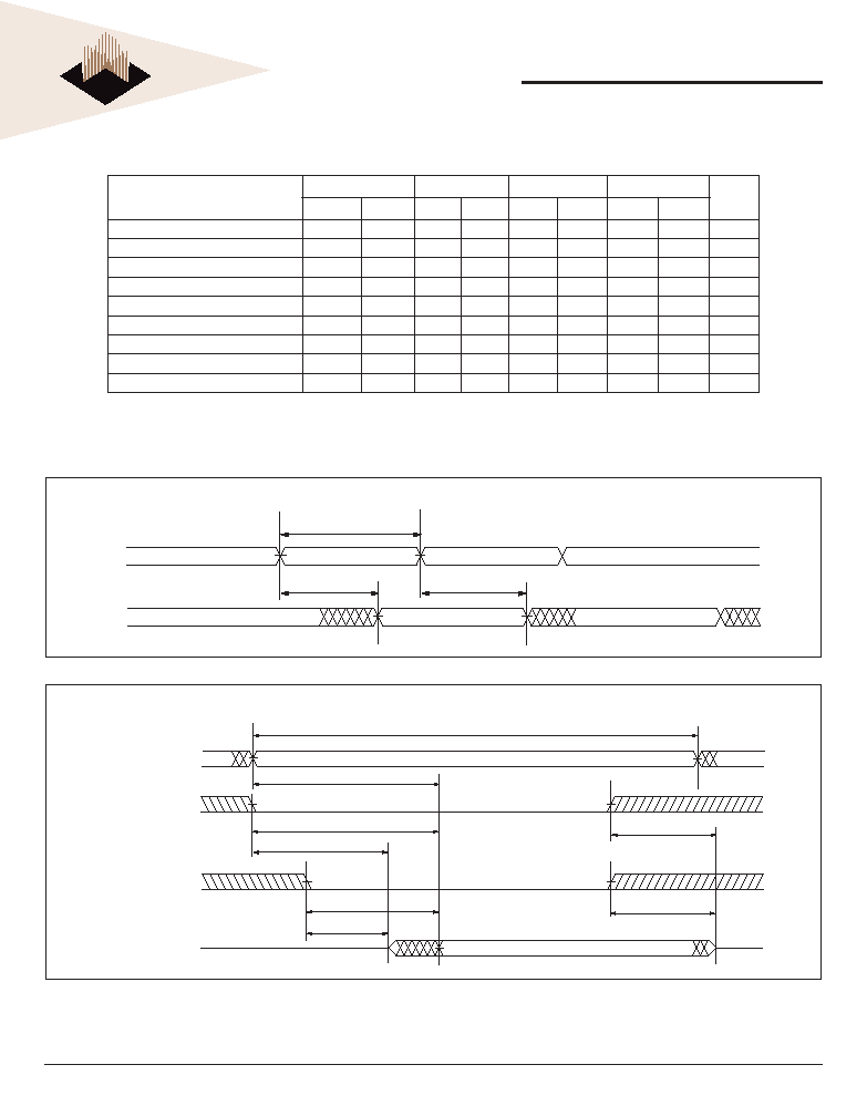
AC CHARACTERISTICS READ CYCLE
Parameter
Symbol
12ns
15ns
20ns
Units
JEDEC
Alt.
Min
Max
Min
Max
Min
Max
Read Cycle Time
t
AVAV
t
RC
12
15
20
ns
Address Access Time
t
AVQV
t
AA
12
15
20
ns
Chip Enable Access Time
t
ELQV
t
ACS
8
10
20
ns
Chip Enable to Output in Low Z (1)
t
ELQX
t
CLZ
2
3
3
ns
Chip Disable to Output in High Z (1)
t
EHQZ
t
CHZ
7
8
10
ns
Output Hold from Address Change
t
AVQX
t
OH
3
3
3
ns
Output Enable to Output Valid
t
GLQV
t
OE
5
6
8
ns
Output Enable to Output in Low Z (1)
t
GLQX
t
OLZ
2
2
2
ns
Output Disable to Output in High Z(1)
t
GHQZ
t
OHZ
4
5
8
ns
READ CYCLE 2 - W# HIGH
READ CYCLE 1 - W# HIGH, G#, E# LOW
Note 1: Parameter guaranteed, but not tested.
A
Q
t
AVAV
ADDRESS 1
t
AVQV
ADDRESS 2
t
AVQX
DATA 1
DATA 2
A
BSx#, E#
G#
Q
t
AVAV
t
AVQV
t
ELQV
t
ELQX
t
GLQV
t
GLQX
t
EHQZ
t
GHQZ
4
White Electronic Designs Corporation ∑ (602) 437-1520 ∑ www.wedc.com
White Electronic Designs
EDI8L32128V
July 2004
Rev. 6
White Electronic Designs Corp. reserves the right to change products or specifi cations without notice.
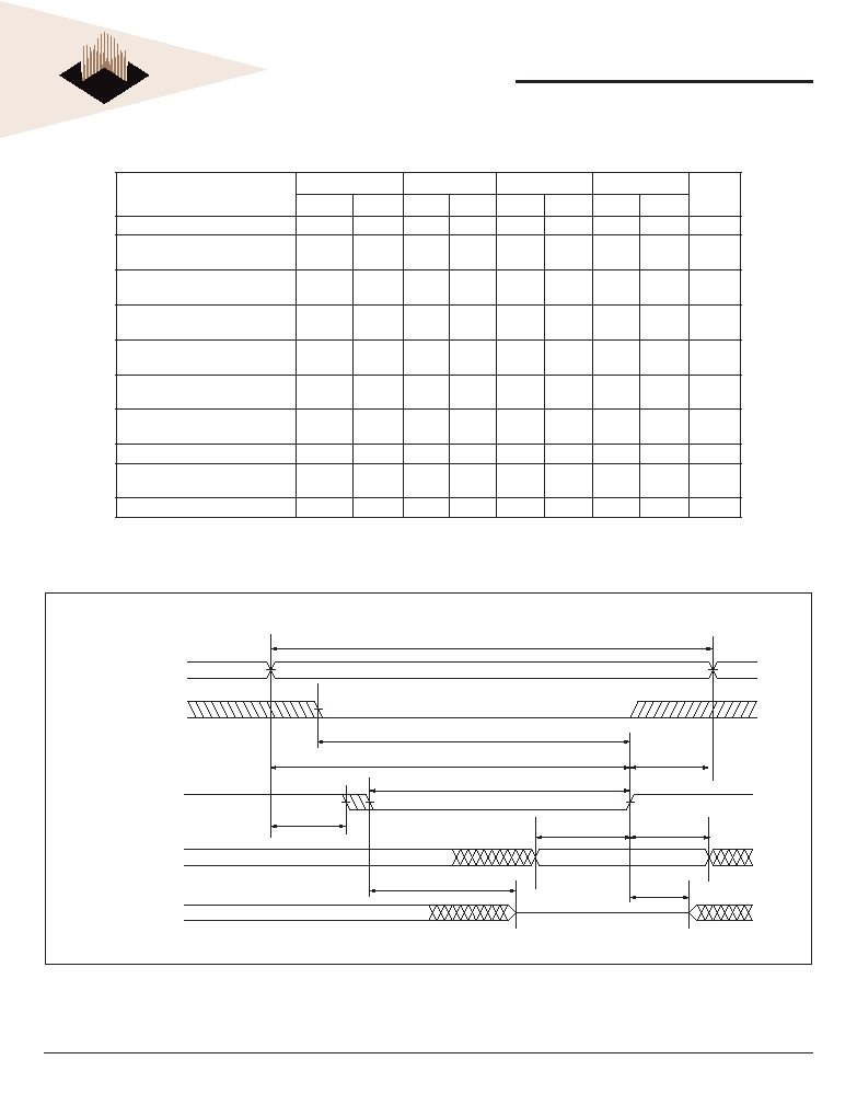
A
BSx#, E#
W#
D
Q
t
AVAV
t
ELWH
t
AVWH
t
WLWH
t
WHAX
t
WHDX
t
DVWH
DATA VALID
t
WHQX
t
WLQZ
t
AVWL
Note 1: Parameter guaranteed, but not tested.
WRITE CYCLE 1 - W# CONTROLLED
Parameter
Symbol
12ns
15ns
20ns
Units
JEDEC
Alt.
Min
Max
Min
Max
Min
Max
Write Cycle Time
t
AVAV
t
WC
12
15
20
ns
Chip Enable to End of Write
t
ELWH
t
ELEH
t
CW
t
CW
8
8
9
9
15
15
ns
ns
Address Setup Time
t
AVWL
t
AVEL
t
AS
t
AS
0
0
0
0
0
0
ns
ns
Address Valid to End of Write
t
AVWH
t
AVEH
t
AW
t
AW
9
9
10
10
15
15
ns
ns
Write Pulse Width
t
WLWH
t
WLEH
t
WP
t
WP
9
9
10
10
15
15
ns
ns
Write Recovery Time
t
WHAX
t
EHAX
t
WR
t
WR
0
0
0
0
0
0
ns
ns
Data Hold Time
t
WHDX
t
EHDX
t
DH
t
DH
0
0
0
0
0
0
ns
ns
Write to Output in High Z (1)
t
WLQZ
t
WHZ
0
5
0
6
0
7
ns
Data to Write Time
t
DVWH
t
DVEH
t
DW
t
DW
5
5
6
6
8
8
ns
ns
Output Active from End of Write (1)
t
WHQX
t
WLZ
2
2
2
ns
AC CHARACTERISTICS WRITE CYCLE
5
White Electronic Designs Corporation ∑ (602) 437-1520 ∑ www.wedc.com
White Electronic Designs
EDI8L32128V
July 2004
Rev. 6
White Electronic Designs Corp. reserves the right to change products or specifi cations without notice.
0.995
Max
0.995
Max
0.956
Max
0.956
Max
0.040
Max
0.020
0.015
0.930
0.890
0.050
BSC
0.115
Max
0.180
Max
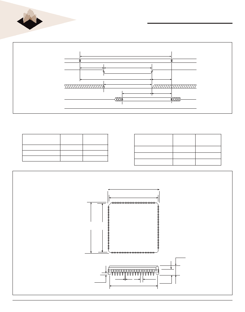
A
BSx#, E#
W#
D
Q
t
AVAV
t
AVEL
t
ELEH
t
AVEH
t
WLEH
t
DVEH
DATA VALID
t
EHAX
t
EHDX
HIGH Z
Package No. 99
68 Lead PLCC
JEDEC MO-47AE
THETA J
A
=40∞C/W
THETA J
C
=15∞C/W
WEIGHT =4.2G
PACKAGE DESCRIPTION
ORDERING INFORMATION
WRITE CYCLE 2 - E# CONTROLLED
Part Number
Speed
(ns)
Package
No.
EDI8L32128V12AC
12
99
EDI8L32128V15AC
15
99
EDI8L32128V20AC
20
99
Part Number
Speed
(ns)
Package
No.
EDI8L32128V12AI
12
99
EDI8L32128V15AI
15
99
EDI8L32128V20AI
20
99
Commercial (0∞C to 70∞C)
Industrial (-40∞C to +85∞C)

6
White Electronic Designs Corporation ∑ (602) 437-1520 ∑ www.wedc.com
White Electronic Designs
EDI8L32128V
July 2004
Rev. 6
White Electronic Designs Corp. reserves the right to change products or specifi cations without notice.
Figure 2
Figure 1
Address Bus
A31 - A0
Analog
ADSP - 2106XL
Databus
D47 - D0
MS0#
WR#
RD#
A16-A0
E0#
E1#
E2#
E3#
W#
G#
D
A
T
A
B
U
S
DQ31
DQ16
DQ15
DQ0
EDI8L32128V
(Configured as 256Kx16)
MS1#
EDI8L32128V
(Configured as 256Kx16)
EDI8L32128V
(Configured as 256Kx16)
D
A
T
A
B
U
S
D
A
T
A
B
U
S
A16-A0
E0#
E1#
E2#
E3#
W#
G#
A16-A0
E0#
E1#
E2#
E3#
W#
G#
DQ31
DQ16
DQ15
DQ0
DQ31
DQ16
DQ15
DQ0
D Q 1 5
W O R D 1
D Q 0
D Q 3 1
W O R D 2
D Q 1 6
D Q 4 7
W O R D 3
D Q 1 7
Address Bus
A31 - A0
Analog
ADSP - 2106XL
Databus
D47 - D0
D47 D46 .. D31 D30 .. D5 D4 D3 D2 D1 D0
MS0#
WR#
RD#
A16
A15
A14
A13
A12
A4
A3
A2
A1
A0
E0#
E1#
E2#
E3#
W#
G#
A
D
D
R
E
S
S
B
U
S
D
A
T
A
B
U
S
DQ31
DQ30
DQ29
DQ28
DQ27
DQ4
DQ3
DQ2
DQ1
DQ0
EDI8L32128V

7
White Electronic Designs Corporation ∑ (602) 437-1520 ∑ www.wedc.com
White Electronic Designs
EDI8L32128V
July 2004
Rev. 6
White Electronic Designs Corp. reserves the right to change products or specifi cations without notice.
Document Title
128Kx32 CMOS High Speed Static RAM
Revision History
Rev #
History
Release Date
Status
Rev 6
6.1 Corrected pin confi guration and block diagram on page 1
6.2 Changed pin 64 from "NC" to "A16"
6.3 Added new title page
7-2004
Final