1
White Electronic Designs Corporation ∑ (602) 437-1520 ∑ www.wedc.com
White Electronic Designs
W3E16M72SR-XBX
February 2005
Rev. 2
16Mx72 Registered DDR SDRAM
Registered for enhanced performance of bus
speeds of 200, 225, and 250 MHz
Package:
∑ 219 Plastic Ball Grid Array (PBGA), 32 x 25mm
2.5V ±0.2V core power supply
2.5V I/O (SSTL_2 compatible)
Differential clock inputs (CK and CK#)
Commands entered on each positive CK edge
Internal pipelined double-data-rate (DDR)
architecture; two data accesses per clock cycle
Programmable Burst length: 2,4 or 8
Bidirectional data strobe (DQS) transmitted/
received with data, i.e., source-synchronous data
capture (one per byte)
DQS edge-aligned with data for READs; center-
aligned with data for WRITEs
DLL to align DQ and DQS transitions with CK
Four internal banks for concurrent operation
Two data mask (DM) pins for masking write data
Programmable
I
OL
/I
OH
option
Auto precharge option
FEATURES
25
32
66
TSOP
66
TSOP
66
TSOP
66
TSOP
66
TSOP
11.9
11.9
11.9
22.3
Monolithic Solution
Actual Size
S
A
V
I
N
G
S
Area
I/O
Count
5 x 265mm2 + 2 x 105mm2 = 1536mm2
5 x 66 pins + 2 x 48 = 426 pins
800mm2
47%
219 Balls
49%
W3E16M72SR-XBX
White Electronic Designs
48
TSOP
12.6
48
TSOP
12.6
8.3
11.9
22.3
22.3
Auto Refresh and Self Refresh Modes
Commercial,
Industrial
and
Military
Temperature
Ranges
Organized as 16M x 72
Weight: W3E16M72SR-XBX - 2.5 grams typical
BENEFITS
47%
SPACE
SAVINGS
Glueless Connection to PCI Bridge/Memory
Controller
Reduced part count
Reduced
I/O
count
∑ 49% I/O Reduction
Reduced trace lengths for lower parasitic
capacitance
Suitable for hi-reliability applications
Laminate interposer for optimum TCE match
Upgradeable to 32M x 72 density (contact factory
for information)
* This product is subject to change without notice.

2
White Electronic Designs Corporation ∑ (602) 437-1520 ∑ www.wedc.com
White Electronic Designs
W3E16M72SR-XBX
February 2005
Rev. 2
FIGURE 1 ≠ PIN CONFIGURATION
NOTE: DNU = Do Not Use; to be left unconnected for future upgrades. Pin D8 will be A13, D9 will be A14, and D10 will be A15 as needed.
NC = Not Connected Internally.
Top View
1
2
3
4
5
6
7
8
9 10
11 12 13 14 15 16
A
B
C
D
E
F
G
H
J
K
L
M
N
P
R
T
DQ1
DQ3
DQ6
DQ7
CAS#
CS#
V
SS
V
SS
CK3#
NC
DQ56
DQ57
DQ60
DQ62
V
SS
VSS
DQ30
DQ28
DQ25
DQ24
CK1
NC
V
CC
V
CC
NC
RV
REF
DQ39
DQ38
DQ35
DQ33
V
CC
DQ0
DQ2
DQ4
DQ5
DM0
WE#
RAS#
V
SS
V
SS
NC
CK3
DM7
DQ58
DQ59
DQ61
DQ63
DQ31
DQ29
DQ27
DQ26
NC
DM3
CK1#
V
CCQ
V
CCQ
NC
RESET#
DM4
DQ37
DQ36
DQ34
DQ32
DQ14
DQ12
DQ10
DQ8
V
CC
V
CC
V
CC
V
CC
V
CC
V
CC
V
CC
V
CC
DQ55
DQ53
DQ51
DQ49
DQ17
DQ19
DQ21
DQ23
V
SS
V
SS
V
SS
V
SS
V
SS
V
SS
V
SS
V
SS
DQ40
DQ42
DQ44
DQ46
DQ15
DQ13
DQ11
DQ9
DM1
CK0
CKE
V
CCQ
V
CCQ
NC
NC
NC
DQ54
DQ52
DQ50
DQ48
DQ16
DQ18
DQ20
DQ22
DM2
RCK0B
RCK1B
V
SS
V
SS
NC
CK2
DM5
DQ41
DQ43
DQ45
DQ47
V
SS
V
SS
V
CC
V
CCQ
DQS7
DQS6
CK0#
V
SS
V
SS
DQS8
NC
DM6
DQS9
V
SS
V
CC
V
CCQ
V
CCQ
V
CC
V
SS
V
SS
V
REF
RCK0
RCK1
V
CC
V
CC
CK2#
DQS4
NC
DQS5
V
CC
V
SS
V
SS
A9
A0
A2
A12
DQS1
DM9
DQ73
DQ75
DQ77
DQ79
A8
A1
A3
DNU
DQS2
NC
DQ70
DQ68
DQ66
DQ64
A10
A7
A5
DNU
BA0
CK4
DQ72
DQ74
DQ76
DQ78
A11
A6
A4
DNU
BA1
NC
DQ71
DQ69
DQ67
DQ65
V
SS
V
SS
V
CC
V
CCQ
DQS0
NC
CK4#
V
SS
V
CC
V
CCQ
V
CCQ
V
CC
V
SS
V
SS
DQS3
NC
DM8
V
CC
V
SS
V
SS

3
White Electronic Designs Corporation ∑ (602) 437-1520 ∑ www.wedc.com
White Electronic Designs
W3E16M72SR-XBX
February 2005
Rev. 2
V
REF
RESET#
A
0-12
BA
0-1
CK
0
#
CK#
CAS#
DQ
0
DQ
15
CKE
B
CKE
DM
0
DQML
DM
1
DQMH
DQ
0
DQ
15
U1
A
0-12
BA
0-1
CK
1
#
CK#
DQ
16
DQ
31
RAS
B
#
WE
B
#
CAS
B
#
DQ
0
DQ
15
WE#
U0
RAS#
CKE
B
CKE
DM
2
DQML
DM
3
DQMH
DQ
0
DQ
15
U2
A
0-12
BA
0-1
CK
2
#
CK#
DQ
32
DQ
47
CKE
B
CKE
DM
4
DQML
DM
5
DQMH
DQ
0
DQ
15
U3
A
0-12
BA
0-1
CK
3
#
CK#
DQ
48
DQ
63
CKE
B
CKE
DQS
6
DQSL
DQS
7
DQSH
DQ
0
DQ
15
U4
A
0-12
BA
0-1
CK
4
#
CK#
DQ
64
DQ
79
CKE
B
CKE
DQS
8
DQSL
DQS
9
DQSH
Y
=
Y
=
Y
=
Y
=
Y
=
Y
=
Y
=
Y
=
Y
=
Y
=
Y
=
Y
=
Y
=
Y
=
Y
=
Y
=
Y
=
Y
=
Y
=
Y
=
Y
=
Y
=
Y
=
Y
=
Y
=
Y
=
Y
=
Y
=
Y
=
Y
=
Y
=
Y
=
Y
=
Y
=
Y
=
Y
=
Y
=
Y
=
Y
=
Y
=
Y
=
Y
=
Y
=
Y
=
Y
=
Y
=
Y
=
Y
=
Y
=
Y
=
Y
=
Y
=
Y
=
Y
=
Y
=
Y
=
Y
=
Y
=
Y
=
Y
=
CK
4
CK
V
REF
CK
3
CK
V
REF
DQS
4
DQSL
DQS
5
DQSH
V
REF
DQS
2
DQSL
DQS
3
DQSH
V
REF
DQS
0
DQSL
DQS
1
DQSH
V
REF
CK
2
CK
CK
1
CK
CK
0
CK
V
REF
DM
6
DQML
DM
7
DQMH
DM
8
DM
9
DQML
DQMH
U5
U6
CAS
B
#
RAS
B
#
WE
B
#
CS
B
#
CKE
B
#
V
REF
RESET#
RAS#
CAS#
WE#
CS#
CKE
RV
REF
RESET#
A
0-12
BA
0
-
1
SSTV16857
SSTV16857
RCK
1
RCK
1B
RCK
0
RCK
0B
CS
B
#
CS#
CAS#
WE# RAS#
CS#
CAS#
WE# RAS#
CS#
CAS#
WE# RAS#
CS#
CAS#
WE# RAS#
CS#
FIGURE 2 ≠ FUNCTIONAL BLOCK DIAGRAM

4
White Electronic Designs Corporation ∑ (602) 437-1520 ∑ www.wedc.com
White Electronic Designs
W3E16M72SR-XBX
February 2005
Rev. 2
The pipelined, multibank architecture of DDR SDRAMs
allows for concurrent operation, thereby providing high
effective bandwidth by hiding row precharge and activation
time.
An auto refresh mode is provided, along with a power-
saving power-down mode.
FUNCTIONAL DESCRIPTION
Read and write accesses to the DDR SDRAM are burst
oriented; accesses start at a selected location and continue
for a programmed number of locations in a programmed
sequence. Accesses begin with the registration of an
ACTIVE command which is then followed by a READ or
WRITE command. The address bits registered coincident
with the ACTIVE command are used to select the bank and
row to be accessed (BA0 and BA1 select the bank, A0-12
select the row). The address bits registered coincident
with the READ or WRITE command are used to select the
starting column location for the burst access.
Prior to normal operation, the SDRAM must be initialized.
The following sections provide detailed information
covering device initialization, register defi nition, command
descriptions and device operation.
INITIALIZATION
DDR SDRAMs must be powered up and initialized in a
predefi ned manner. Operational procedures other than
those specifi ed may result in undefi ned operation. Power
must fi rst be applied to V
CC
and V
CCQ
simultaneously, and
then to V
REF
(and to the system V
TT
). V
TT
must be applied
after V
CCQ
to avoid device latch-up, which may cause
permanent damage to the device. V
REF
can be applied any
time after V
CCQ
but is expected to be nominally coincident
with V
TT
. Except for CKE, inputs are not recognized as
valid until after V
REF
is applied. CKE is an SSTL_2 input
but will detect an LVCMOS LOW level after V
CC
is applied.
Maintaining an LVCMOS LOW level on CKE during power-
up is required to ensure that the DQ and DQS outputs will
be in the High-Z state, where they will remain until driven
in normal operation (by a read access). After all power
supply and reference voltages are stable, and the clock
is stable, the DDR SDRAM requires a 200µs delay prior
to applying an executable command.
GENERAL DESCRIPTION
The 128MByte (1Gb) DDR SDRAM is a high-speed CMOS,
dynamic random-access, memory using 5 chips containing
268,435,456 bits. Each chip is internally confi gured as a
quad-bank DRAM. Each of the chip's 67,108,864-bit banks
is organized as 8,192 rows by 512 columns by 16 bits.
The 128 MB DDR SDRAM uses a double data rate
architecture to achieve high-speed operation. The
double data rate architecture is essentially a 2n-prefetch
architecture with an interface designed to transfer two data
words per clock cycle at the I/O pins. A single read or write
access for the 128MB DDR SDRAM effectively consists
of a single 2n-bit wide, one-clock-cycle data tansfer at the
internal DRAM core and two corresponding n-bit wide,
one-half-clock-cycle data transfers at the I/O pins.
A bidirectional data strobe (DQS) is transmitted externally,
along with data, for use in data capture at the receiver. DQS
is a strobe transmitted by the DDR SDRAM during READs
and by the memory contoller during WRITEs. DQS is edge-
aligned with data for READs and center-aligned with data
for WRITEs. Each chip has two data strobes, one for the
lower byte and one for the upper byte.
The 128MB DDR SDRAM operates from a differential clock
(CK and CK#); the crossing of CK going HIGH and CK#
going LOW will be referred to as the positive edge of CK.
Commands (address and control signals) are registered
at every positive edge of CK. Input data is registered on
both edges of DQS, and output data is referenced to both
edges of DQS, as well as to both edges of CK.
Read and write accesses to the DDR SDRAM are burst
oriented; accesses start at a selected location and continue
for a programmed number of locations in a programmed
sequence. Accesses begin with the registration of an
ACTIVE command, which is then followed by a READ or
WRITE command. The address bits registered coincident
with the ACTIVE command are used to select the bank
and row to be accessed. The address bits registered
coincident with the READ or WRITE command are used
to select the bank and the starting column location for the
burst access.
The DDR SDRAM provides for programmable READ
or WRITE burst lengths of 2, 4, or 8 locations. An auto
precharge function may be enabled to provide a self-
timed row precharge that is initiated at the end of the
burst access.

5
White Electronic Designs Corporation ∑ (602) 437-1520 ∑ www.wedc.com
White Electronic Designs
W3E16M72SR-XBX
February 2005
Rev. 2
Once the 200µs delay has been satisfi ed, a DESELECT
or NOP command should be applied, and CKE should
be brought HIGH. Following the NOP command, a
PRECHARGE ALL command should be applied. Next a
LOAD MODE REGISTER command should be issued for
the extended mode register (BA1 LOW and BA0 HIGH)
to enable the DLL, followed by another LOAD MODE
REGISTER command to the mode register (BA0/BA1
both LOW) to reset the DLL and to program the operating
parameters. Two-hundred clock cycles are required
between the DLL reset and any READ command. A
PRECHARGE ALL command should then be applied,
placing the device in the all banks idle state.
Once in the idle state, two AUTO REFRESH cycles must
be performed (t
RFC
must be satisfi ed.) Additionally, a LOAD
MODE REGISTER command for the mode register with
the reset DLL bit deactivated (i.e., to program operating
parameters without resetting the DLL) is required.
Following these requirements, the DDR SDRAM is ready
for normal operation.
REGISTER DEFINITION
MODE REGISTER
The Mode Register is used to defi ne the specifi c mode of
operation of the DDR SDRAM. This defi nition includes the
selection of a burst length, a burst type, a CAS latency,
and an operating mode, as shown in Figure 3. The Mode
Register is programmed via the MODE REGISTER SET
command (with BA0 = 0 and BA1 = 0) and will retain
the stored information until it is programmed again or
the device loses power. (Except for bit A8 which is self
clearing).
Reprogramming the mode register will not alter the contents
of the memory, provided it is performed correctly. The
Mode Register must be loaded (reloaded) when all banks
are idle and no bursts are in progress, and the controller
must wait the specifi ed time before initiating the subsequent
operation. Violating either of these requirements will result
in unspecifi ed operation.
Mode register bits A0-A2 specify the burst length, A3
specifi es the type of burst (sequential or interleaved),
A4-A6 specify the CAS latency, and A7-A12 specify the
operating mode.
BURST LENGTH
Read and write accesses to the DDR SDRAM are burst
oriented, with the burst length being programmable,
as shown in Figure 3. The burst length determines
the maximum number of column locations that can be
accessed for a given READ or WRITE command. Burst
lengths of 2, 4 or 8 locations are available for both the
sequential and the interleaved burst types.
Reserved states should not be used, as unknown operation
or incompatibility with future versions may result.
When a READ or WRITE command is issued, a block of
columns equal to the burst length is effectively selected. All
accesses for that burst take place within this block, meaning
that the burst will wrap within the block if a boundary is
reached. The block is uniquely selected by A1-Ai when the
burst length is set to two; by A2-Ai when the burst length
is set to four (where Ai is the most signifi cant column
address for a given confi guration); and by A3-Ai when the
burst length is set to eight. The remaining (least signifi cant)
address bit(s) is (are) used to select the starting location
within the block. The programmed burst length applies to
both READ and WRITE bursts.
BURST TYPE
Accesses within a given burst may be programmed to be
either sequential or interleaved; this is referred to as the
burst type and is selected via bit M3.
The ordering of accesses within a burst is determined by
the burst length, the burst type and the starting column
address, as shown in Table 1.
READ LATENCY
The READ latency is the delay, in clock cycles, between
the registration of a READ command and the availability
of the fi rst bit of output data. The latency can be set to 2
or 2.5 clocks.
If a READ command is registered at clock edge n, and the
latency is m clocks, the data will be available by clock edge
n+m. Table 2 below indicates the operating frequencies at
which each CAS latency setting can be used.
Reserved states should not be used as unknown operation
or incompatibility with future versions may result.

6
White Electronic Designs Corporation ∑ (602) 437-1520 ∑ www.wedc.com
White Electronic Designs
W3E16M72SR-XBX
February 2005
Rev. 2
EXTENDED MODE REGISTER
The extended mode register controls functions beyond
those controlled by the mode register; these additional
functions are DLL enable/disable, output drive strength,
and QFC#. These functions are controlled via the bits
shown in Figure 5. The extended mode register is
programmed via the LOAD MODE REGISTER command
to the mode register (with BA
0
= 1 and BA
1
= 0) and
will retain the stored information until it is programmed
again or the device loses power. The enabling of the DLL
should always be followed by a LOAD MODE REGISTER
command to the mode register (BA
0
/BA
1
both LOW) to
reset the DLL.
The extended mode register must be loaded when all
banks are idle and no bursts are in progress, and the
controller must wait the specifi ed time before initiating
any subsequent operation. Violating either of these
requirements could result in unspecifi ed operation.
FIGURE 3 ≠ MODE REGISTER DEFINITION
M3 = 0
2
4
8
Reserved
Reserved
Reserved
M3 = 1
2
4
8
Reserved
Reserved
Reserved
Reserved
Operating Mode
Normal Operation
Normal Operation/Reset DLL
All other states reserved
0
0
Valid
Valid
0
1
Burst Type
Sequential
Interleaved
CAS Latency
Reserved
Reserved
2
Reserved
Reserved
2.5
Reserved
Burst Length
M0
0
1
0
1
0
1
0
1
Burst Length
CAS Latency BT
A9
A7 A6
A5 A4 A3
A8
A2
A1 A0
Mode Register (Mx)
Address Bus
M1
0
0
1
1
0
0
1
1
M2
0
0
0
0
1
1
1
1
M3
M4
0
1
0
1
0
1
0
1
M5
0
0
1
1
0
0
1
1
M6
0
0
0
0
1
1
1
1
M6-M0
M8
M7
Operating Mode
A10
A11
* M14 and M13
(BA0 and BA1 must be
"0, 0" to select
the base mode register
(vs. the extended
mode
register).
0*
0*
BA0
BA1
Reserved
Reserved
Reserved
Reserved
M9
M10
M11
0
0
0
1
0
0
0
0
-
-
-
-
-
-
A12
M12
0
0
-
TABLE 2 ≠ CAS LATENCY
SPEED
ALLOWABLE OPERATING
FREQUENCY (MHz)
CAS
LATENCY = 2
CAS
LATENCY = 2.5
-200
75
100
-225
100
112.5
-250
100
125
OPERATING MODE
The normal operating mode is selected by issuing a MODE
REGISTER SET command with bits A7-A12 each set to
zero, and bits A0-A6 set to the desired values. A DLL reset
is initiated by issuing a MODE REGISTER SET command
with bits A7 and A9-A12 each set to zero, bit A8 set to one,
and bits A0-A6 set to the desired values. Although not
required, JEDEC specifi cations recommend when a LOAD
MODE REGISTER command is issued to reset the DLL, it
should always be followed by a LOAD MODE REGISTER
command to select normal operating mode.
All other combinations of values for A7-A12 are reserved
for future use and/or test modes. Test modes and reserved
states should not be used because unknown operation or
incompatibility with future versions may result.
TABLE 1 ≠ BURST DEFINITION
Burst
Length
Starting Column
Address
Order of Accesses Within a Burst
Type = Sequential
Type = In ter leaved
2
A0
0
0-1
0-1
1
1-0
1-0
4
A1
A0
0
0
0-1-2-3
0-1-2-3
0
1
1-2-3-0
1-0-3-2
1
0
2-3-0-1
2-3-0-1
1
1
3-0-1-2
3-2-1-0
8
A2
A1
A0
0
0
0
0-1-2-3-4-5-6-7
0-1-2-3-4-5-6-7
0
0
1
1-2-3-4-5-6-7-0
1-0-3-2-5-4-7-6
0
1
0
2-3-4-5-6-7-0-1
2-3-0-1-6-7-4-5
0
1
1
3-4-5-6-7-0-1-2
3-2-1-0-7-6-5-4
1
0
0
4-5-6-7-0-1-2-3
4-5-6-7-0-1-2-3
1
0
1
5-6-7-0-1-2-3-4
5-4-7-6-1-0-3-2
1
1
0
6-7-0-1-2-3-4-5
6-7-4-5-2-3-0-1
1
1
1
7-0-1-2-3-4-5-6
7-6-5-4-3-2-1-0
NOTES:
1.
For a burst length of two, A
1
-Ai select two-data-element block; A
0
selects the
starting column within the block.
2.
For a burst length of four, A
2
-Ai select four-data-element block; A
0-1
select the
starting column within the block.
3.
For a burst length of eight, A
3
-Ai select eight-data-element block; A
0-2
select the
starting column within the block.
4.
Whenever a boundary of the block is reached within a given sequence above, the
following access wraps within the block.

7
White Electronic Designs Corporation ∑ (602) 437-1520 ∑ www.wedc.com
White Electronic Designs
W3E16M72SR-XBX
February 2005
Rev. 2
DESELECT
The DESELECT function (CS# HiGH) prevents new
commands from being executed by the DDR SDRAM. The
SDRAM is effectively deselected. Operations already in
progress are not affected.
NO OPERATION (NOP)
The NO OPERATION (NOP) command is used to perform
a NOP to the selected DDR SDRAM (CS# is LOW). This
prevents unwanted commands from being registered
during idle or wait states. Operations already in progress
are not affected.
LOAD MODE REGISTER
The Mode Registers are loaded via inputs A
0-12
. The LOAD
MODE REGISTER command can only be issued when all
banks are idle, and a subsequent executable command
cannot be issued until t
MRD
is met.
COMMAND READ
NOP
NOP
NOP
CL = 2.5
DON'T CARE
TRANSITIONING DATA
DQ
DQS
T0 T1 T2
T2n
T3
T3n
COMMAND READ
NOP
NOP
NOP
CL = 2
DQ
DQS
CLK
CLK#
T0 T1 T2
T2n
T3
T3n
Burst Length = 4 in the cases shown
Shown with nominal tAC and nominal tDSDQ
DATA
CLK
CLK#
OUTPUT DRIVE STRENGTH
The normal full drive strength for all outputs are specifi ed to
be SSTL2, Class II. The DDR SDRAM supports an option
for reduced drive. This option is intended for the support
of the lighter load and/or point-to-point environments. The
selection of the reduced drive strength will alter the DQs
and DQSs from SSTL2, Class II drive strength to a reduced
drive strength, which is approximately 54 percent of the
SSTL2, Class II drive strength.
DLL ENABLE/DISABLE
The DLL must be enabled for normal operation. DLL
enable is required during power-up initialization and upon
returning to normal operation after having disabled the DLL
for the purpose of debug or evaluation. (When the device
exits self refresh mode, the DLL is enabled automatically.)
Any time the DLL is enabled, 200 clock cycles must occur
before a READ command can be issued.
COMMANDS
The Truth Table provides a quick reference of available
commands. This is followed by a written description of
each command.
FIGURE 4 ≠ CAS LATENCY
FIGURE 5 ≠ EXTENDED MODE REGISTER
DEFINITION
DLL
Enable
Disable
DLL
DS
A
9
A
7
A
6
A
5
A
4
A
3
A
8
A
2
A
1
A
0
Extended Mode
Register (Ex)
Address Bus
Operating Mode
A
10
A
11
11
01
BA
0
BA
1
QFC#
E0
0
1
Drive Strength
Normal
Reduced
E1
0
1
QFC# Function
Disabled
Reserved
E22
0
-
Operating Mode
Reserved
Reserved
E2, E1, E0
Valid
-
E12
0
-
E10
0
-
E9
0
-
E8
0
-
E7
0
-
E6
0
-
E5
0
-
E4
0
-
E3
0
-
A
12
E11
0
-
1. E14 and E13 must be "0, 1" to select the Extended Mode Register (vs. the base Mode Register)
2. The QFE# function is not supported.

8
White Electronic Designs Corporation ∑ (602) 437-1520 ∑ www.wedc.com
White Electronic Designs
W3E16M72SR-XBX
February 2005
Rev. 2
NOTES:
1. CKE is HIGH for all commands shown except SELF REFRESH.
2. A
0-12
defi ne the op-code to be written to the selected Mode Register. BA
0
, BA
1
select either the mode register (0, 0) or the extended mode register (1, 0).
3. A
0-12
provide row address, and BA
0
, BA
1
provide bank address.
4. A
0-8
provide column address; A
10
HIGH enables the auto precharge feature (non
persistent), while A
10
LOW disables the auto precharge feature; BA
0
, BA
1
provide
bank address.
5. A
10
LOW: BA
0
, BA
1
determine the bank being precharged. A
10
HIGH: All banks
precharged and BA
0
, BA
1
are "Don't Care."
6. This command is AUTO REFRESH if CKE is HIGH; SELF REFRESH if CKE is
LOW.
7. Internal refresh counter controls row addressing; all inputs and I/Os are "Don't
Care" except for CKE.
8. Applies only to read bursts with auto precharge disabled; this command is
undefi ned (and should not be used) for READ bursts with auto precharge enabled
and for WRITE bursts.
9. DESELECT and NOP are functionally interchangeable.
10. Used to mask write data; provided coincident with the corresponding data.
ACTIVE
The ACTIVE command is used to open (or activate) a
row in a particular bank for a subsequent access. The
value on the BA
0
, BA
1
inputs selects the bank, and the
address provided on inputs A
0-12
selects the row. This row
remains active (or open) for accesses until a PRECHARGE
command is issued to that bank. A PRECHARGE
command must be issued before opening a different row
in the same bank.
READ
The READ command is used to initiate a burst read access
to an active row. The value on the BA
0
, BA
1
inputs selects
the bank, and the address provided on inputs A
0-8
selects
the starting column location. The value on input A
10
determines whether or not AUTO PRECHARGE is used. If
AUTO PRECHARGE is selected, the row being accessed
will be precharged at the end of the READ burst; if AUTO
PRECHARGE is not selected, the row will remain open
for subsequent accesses.
WRITE
The WRITE command is used to initiate a burst write
access to an active row. The value on the BA0, BA1 inputs
selects the bank, and the address provided on inputs A0-8
selects the starting column location. The value on input A10
determines whether or not AUTO PRECHARGE is used. If
AUTO PRECHARGE is selected, the row being accessed
will be precharged at the end of the WRITE burst; if AUTO
PRECHARGE is not selected, the row will remain open for
subsequent accesses. Input data appearing on the D/Qs
is written to the memory array subject to the DQM input
logic level appearing coincident with the data. If a given
DQM signal is registered LOW, the corresponding data
REGISTER FUNCTION TABLE
INPUTS
OUTPUT
Q
RESET#
RCK
RCK#
INPUT
H
H
H
H
L
L
H
L or H
L or H
X
Q
0
L
X, or fl oating
X, or fl oating
X, or fl oating
L
TRUTH TABLE ≠ COMMANDS (NOTE 1)
NAME (FUNCTION)
CS#
RAS#
CAS#
WE#
ADDR
DESELECT
(NOP)
(9)
H X X X X
NO OPERATION (NOP) (9)
L
H
H
H
X
ACTIVE (Select bank and activate row) (3)
L
L
H
H
Bank/Row
READ (Select bank and column, and start READ burst) (4)
L
H
L
H
Bank/Col
WRITE (Select bank and column, and start WRITE burst) (4)
L
H
L
L
Bank/Col
BURST
TERMINATE
(8)
L H H L X
PRECHARGE (Deactivate row in bank or banks) ( 5)
L
L
H
L
Code
AUTO REFRESH or SELF REFRESH (Enter self refresh mode) (6, 7)
L
L
L
H
X
LOAD MODE REGISTER (2)
L
L
L
L
Op-Code
TRUTH TABLE ≠ DM OPERATION
NAME (FUNCTION)
DM
DQs
WRITE ENABLE (10)
L
Valid
WRITE INHIBIT (10)
H
X

9
White Electronic Designs Corporation ∑ (602) 437-1520 ∑ www.wedc.com
White Electronic Designs
W3E16M72SR-XBX
February 2005
Rev. 2
will be written to memory; if the DQM signal is registered
HIGH, the corresponding data inputs will be ignored, and a
WRITE will not be executed to that byte/column location.
PRECHARGE
The PRECHARGE command is used to deactivate the
open row in a particular bank or the open row in all banks.
The bank(s) will be available for a subsequent row access
a specifi ed time (t
RP
) after the PRECHARGE command is
issued. Except in the case of concurrent auto precharge,
where a READ or WRITE command to a different bank is
allowed as long as it does not interrupt the data transfer
in the current bank and does not violate any other timing
parameters. Input A10 determines whether one or all
banks are to be precharged, and in the case where only
one bank is to be precharged, inputs BA0, BA1 select the
bank. Otherwise BA0, BA1 are treated as "Don't Care."
Once a bank has been precharged, it is in the idle state and
must be activated prior to any READ or WRITE commands
being issued to that bank. A PRECHARGE command will
be treated as a NOP if there is no open row in that bank
(idle state), or if the previously open row is already in the
process of precharging.
AUTO PRECHARGE
AUTO PRECHARGE is a feature which performs the
same individual-bank PRECHARGE function described
above, but without requiring an explicit command. This is
accomplished by using A
10
to enable AUTO PRECHARGE
in conjunction with a specifi c READ or WRITE command.
A precharge of the bank/row that is addressed with the
READ or WRITE command is automatically performed
upon completion of the READ or WRITE burst. AUTO
PRECHARGE is nonpersistent in that it is either enabled
or disabled for each individual READ or WRITE command.
The device supports concurrent auto precharge if the
command to the other bank does not interrupt the data
transfer to the current bank.
AUTO PRECHARGE ensures that the precharge is initiated
at the earliest valid stage within a burst. This "earliest valid
stage" is determined as if an explicit precharge command
was issued at the earliest possible time, without violating
t
RAS
(MIN).The user must not issue another command to
the same bank until the precharge time (t
RP
) is completed.
This is determined as if an explicit PRECHARGE command
was issued at the earliest possible time, without violating
t
RAS
(MIN).
BURST TERMINATE
The BURST TERMINATE command is used to truncate
READ bursts (with auto precharge disabled). The most
recently registered READ command prior to the BURST
TERMINATE command will be truncated. The open page
which the READ burst was terminated from remains
open.
AUTO REFRESH
AUTO REFRESH is used during normal operation of the
DDR SDRAM and is analogous to CAS#-BEFORE-RAS#
(CBR) REFRESH in conventional DRAMs. This command
is nonpersistent, so it must be issued each time a refresh
is required.
The addressing is generated by the internal refresh
controller. This makes the address bits "Don't Care" during
an AUTO REFRESH command. Each DDR SDRAM
requires AUTO REFRESH cycles at an average interval
of 7.8125
µs (maximum).
To allow for improved efficiency in scheduling and
switching between tasks, some fl exibility in the absolute
refresh interval is provided. A maximum of eight AUTO
REFRESH commands can be posted to any given DDR
SDRAM, meaning that the maximum absolute interval
between any AUTO REFRESH command and the next
AUTO REFRESH command is 9 x 7.8125
µs (70.3µs). This
maximum absolute interval is to allow future support for
DLL updates internal to the DDR SDRAM to be restricted
to AUTO REFRESH cycles, without allowing excessive
drift in t
AC
between updates.
Although not a JEDEC requirement, to provide for future
functionality features, CKE must be active (High) during
the AUTO REFRESH period. The AUTO REFRESH period
begins when the AUTO REFRESH command is registered
and ends t
RFC
later.

10
White Electronic Designs Corporation ∑ (602) 437-1520 ∑ www.wedc.com
White Electronic Designs
W3E16M72SR-XBX
February 2005
Rev. 2
REGISTER ELECTRICAL CHARACTERISTICS
Parameter
Test Conditions
V
CC
and V
CCQ
Min
Typ
Max
Unit
I
I
All inputs
V
I
= V
CC
or GND
2.7V
-5
+5
µA
I
CC
Static standby
RESET# = GND
2.7V
10
µA
Static operating
RESET# = V
CC
, V
I
= V
IH
(AC) or V
IL
(AC)
I
O
= 0
112
mA
I
CCD
Dynamic operating
≠ clock only
RESET# = V
CC
, V
I
= V
IH
(AC) or V
IL
(AC), CK and CK# switching
50% duty cycle
I
O
= 0
2.5V
56
µA/ MHz
Dynamic operating
≠ per each data input
RESET# = V
CC
, V
I
= V
IH
(AC) or V
IL
(AC). CK and CK#
switching 50% duty cycle. All data input switching at one-half
clock frequency, 50% duty cycle
180
µA/clock
MHz
Note: All typical values are at V
CC
= 2.5V, T
A
= 25∞C.
NOTE: Stress greater than those listed under "Absolute Maximum Ratings" may cause permanent damage to the device. This is a stress rating only and functional operation of
the device at these or any other conditions greater than those indicated in the operational sections of this specifi cation is not implied. Exposure to absolute maximum rating
conditions for extended periods may affect reliability.
SELF REFRESH*
The SELF REFRESH command can be used to retain
data in the DDR SDRAM, even if the rest of the system is
powered down. When in the self refresh mode, the DDR
SDRAM retains data without external clocking. The SELF
REFRESH command is initiated like an AUTO REFRESH
command except CKE is disabled (LOW). The DLL is
automatically disabled upon entering SELF REFRESH and
is automatically enabled upon exiting SELF REFRESH (200
clock cycles must then occur before a READ command
can be issued). Input signals except CKE are "Don't Care"
during SELF REFRESH.
The procedure for exiting self refresh requires a sequence
of commands. First, CK must be stable prior to CKE going
back HIGH. Once CKE is HIGH, the DDR SDRAM must
have NOP commands issued for t
XSNR
, because time
is required for the completion of any internal refresh in
progress.
A simple algorithm for meeting both refresh and DLL
requirements is to apply NOPs for 200 clock cycles before
applying any other command.
* Self refresh available in commercial and industrial temperatures only.
REGISTER RECOMMENDED OPERATING CONDITIONS
Parameter/Condition
Min
Max
Unit
V
IH
AC high-level input voltage
Data inputs V
REF
+310mV
V
V
IL
AC low-level input voltage
Data inputs
V
REF
-310mV
V
V
IH
High-level
input
voltage
RESET#
1.7
V
V
IL
Low-level
input
voltage
RESET#
0.7
V
Note: The RESET# input of the device must be held at a valid logic level (not fl oating) to ensure proper
device operation.
ABSOLUTE MAXIMUM RATINGS
Parameter
Unit
Voltage on V
CC
, V
CCQ
Supply relative to Vss
-1 to 3.6
V
Voltage on I/O pins relative to V
SS
-1 to 3.6
V
Operating Temperature T
A
(Mil)
-55 to +125
∞C
Operating Temperature T
A
(Ind)
-40 to +85
∞C
Storage Temperature, Plastic
-55 to +125
∞C
CAPACITANCE (NOTE 13)
Parameter
Symbol
Max
Unit
Input Capacitance: CK/CK#
C
I1
8 pF
Addresses, BA0-1 Input Capacitance
C
A
10
pF
Input Capacitance: All other input-only pins
C
I2
9 pF
Input/Output Capacitance: I/Os
C
IO
10 pF
BGA THERMAL RESISTANCE
Description
Symbol
Max
Units
Notes
Junction to Ambient (No Airfl ow)
Theta JA
14.2
∞
C/W
1
Junction to Ball
Theta JB
10.8
∞
C/W
1
Junction to Case (Top)
Theta JC
4.1
∞
C/W
1
Note 1: Refer to AN #0001 at www.whiteedc.com in the application notes
section for modeling conditions.

11
White Electronic Designs Corporation ∑ (602) 437-1520 ∑ www.wedc.com
White Electronic Designs
W3E16M72SR-XBX
February 2005
Rev. 2
DDR DC ELECTRICAL CHARACTERISTICS AND OPERATING CONDITIONS (NOTES 1, 6)
V
CC
= +2.5V ± 0.2V; -55∞C
T
A
+125∞C
Parameter/Condition
Symbol
Min
Max
Units
Supply Voltage
V
CC
2.3
2.7
V
I/O Supply Voltage
V
CCQ
2.3
2.7
V
Input Hight Voltage: Logic 1; All inputs (21)
V
IH
V
REF
+ 0.15
V
CC
+ 0.3
V
Input Low Voltage: Logic 0; All inputs (21)
V
IL
-0.4
V
REF
- 0.15
V
Input Leakage Current: Any input 0V V
IN
V
CC
(All other pins not under test = 0V)
I
I
-2
2
µA
Output Leakage Current: I/Os are disabled; 0V V
OUT
V
CC
I
OZ
-5
5
µA
Output Levels: Full drive option - x16
High Current (V
OUT
= V
CCQ
- 0.373V, minimum V
REF
, minimum V
TT
)
Low Current (V
OUT
= 0.373V, maximum V
REF
, maximum V
TT
)
I
OH
-16.8
≠
mA
I
OL
16.8
≠
mA
Output Levels: Reduced drive option - 16 only
High Current (V
OUT
= V
CCQ
- 0.763V, minimum V
REF
, minimum V
TT
)
Low Current (V
OUT
= 0.763V, maximum V
REF
, maximum V
TT
)
I
OHR
-9
≠
mA
I
OLR
9
≠
mA
I/O Reference Voltage
V
REF
0.49 x V
CCQ
0.51 x V
CCQ
V
I/O Termination Voltage
V
TT
V
REF
- 0.04
V
REF
+ 0.04
V
DDR I
CC
SPECIFICATIONS AND CONDITIONS (NOTES 1-5, 10, 12, 14, 54)
V
CC
= +2.5V ± 0.2V; -55∞C
T
A
+125∞C
Parameter/Condition
Symbol
Max
250Mbps
266Mbps 200Mbps
Units
OPERATING CURRENT: One bank; Active-Precharge; t
RC
= t
RC
(MIN); t
CK
= t
CK
(MIN); DQ, DM, and DQS inputs changing once
per clock cyle; Address and control inputs changing once every two clock cycles; (22, 48)
I
CC0
625
600
mA
OPERATING CURRENT: One bank; Active-Read-Precharge; Burst = 2; t
RC
= t
RC
(MIN); t
CK
= t
CK
(MIN); I
OUT
= 0mA; Address and
control inputs changing once per clock cycle (22, 48)
I
CC1
850
775
mA
PRECHARGE POWER-DOWN STANDBY CURRENT: All banks idle; Power-down mode; t
CK
= t
CK
(MIN); CKE = LOW; (23, 32, 50)
I
CC2P
20
20
mA
IDLE STANDBY CURRENT: CS# = HIGH; All banks idle; t
CK
= t
CK
(MIN); CKE = HIGH; Address and other control inputs changing
once per clock cycle. V
IN
= V
REF
for DQ, DQS, and DM (51)
I
CC2F
225
225
mA
ACTIVE POWER-DOWN STANDBY CURRENT: One bank active; Power-down mode; t
CK
= t
CK
(MIN); CKE = LOW (23, 32, 50)
I
CC3P
150
150
mA
ACTIVE STANDBY CURRENT: CS# = HIGH; CKE = HIGH; One bank; Active-Precharge; t
RC
= t
RAS
(MAX); t
CK
= t
CK
(MIN); DQ,
DM, and DQS inputs changing twice per clock cycle; Address and other control inputs changing once per clock cycle (22)
I
CC3N
250
250
mA
OPERATING CURRENT: Burst = 2; Reads; Continuous burst; One bank active; Address and control inputs changing once per
clock cycle; t
CK
= t
CK
(MIN); I
OUT
= 0mA (22, 48)
I
CC4R
925
925
mA
OPERATING CURRENT: Burst = 2; Writes; Continuous burst; One bank active; Address and control inputs changing once per
clock cycle; t
CK
= t
CK
(MIN); DQ, DM, and DQS inputs changing twice per clock cycle (22)
I
CC4W
800
800
mA
AUTO REFRESH CURRENT
t
REF
= t
RC
(MIN) (27, 50)
I
CC5
1225
1225
mA
t
REF
= 7.8125µs (27, 50)
I
CC5A
30
30
mA
SELF REFRESH CURRENT: CKE 0.2V
Standard (11)
I
CC6
20
20
mA
OPERATING CURRENT: Four bank interleaving READs (BL=4) with auto precharge, t
RC
=t
RC
(MIN); t
CK
= t
CK
(MIN); Address and
control inputs change only during Active READ or WRITE commands. (22, 49)
I
CC7
2000
2000
mA

12
White Electronic Designs Corporation ∑ (602) 437-1520 ∑ www.wedc.com
White Electronic Designs
W3E16M72SR-XBX
February 2005
Rev. 2
ELECTRICAL CHARACTERISTICS AND RECOMMENDED AC OPERATING CHARACTERISTICS
(NOTES 1-5, 14-17, 33)
Parameter
Symbol
266Mbps CL2.5
200Mbps CL2
250Mbps CL2.5
200Mbps CL2
200Mbps CL2.5
150Mbps CL2
Units
Min
Max
Min
Max
Min
Max
Access window of DQs from CLK/CLK#
t
AC
-0.75
+0.75
-0.75
+0.75
-0.75
+0.75
ns
CLK high-level width (30)
t
CH
0.45
0.55 0.45
0.55
0.45
0.55
t
CK
CLK low-level width (30)
t
CL
0.45
0.55
0.45
0.55
0.45
0.55
t
CK
Clock cycle time
CL = 2.5 (45, 52)
t
CK
(2.5)
8
13
9
13
10
13
ns
CL = 2 (45, 52)
t
CK
(2)
10
13
10
13
13
15
ns
DQ and DM input hold time relative to DQS (26, 31)
t
DH
0.5
0.5
0.5
ns
DQ and DM input setup time relative to DQS (26, 31)
t
DS
0.5
0.5
0.5
ns
DQ and DM input pulse width (for each input) (31)
t
DIPW
1.75
1.75
1.75
ns
Access window of DQS from CLK/CLK#
t
DQSCK
-0.75
+0.75
-0.8
+0.8 -0.8
+0.8 ns
DQS input high pulse width
t
DQSH
0.35
0.35
0.35
t
CK
DQS input low pulse width
t
DQSL
0.35
0.35
0.35
t
CK
DQS-DQ skew, DQS to last DQ valid, per group, per access (25, 26)
t
DQSQ
0.5
0.5
0.5
ns
Write command to fi rst DQS latching transition
t
DQSS
0.75
1.25
0.75
1.25
0.75
1.25
t
CK
DQS falling edge to CLK rising - setup time
t
DSS
0.2
0.2
0.2
t
CK
DQS falling edge from CLK rising - hold time
t
DSH
0.2
0.2
0.2
t
CK
Half clock period (34)
t
HP
t
CH
, t
CL
t
CH
, t
CL
t
CH
, t
CL
ns
Data-out high-impedance window from CLK/CLK# (18, 42)
t
HZ
+0.75
+0.75
+0.75
ns
Data-out low-impedance window from CLK/CLK# (18, 43)
t
LZ
-0.75
-0.75
-0.75
ns
Address and control input hold time (fast slew rate) (14)
t
IHF
0.90
0.90
0.90
ns
Address and control input setup time (fast slew rate) (14)
t
ISF
0.90
0.90
0.90
ns
Address and control input hold time (slow slew rate) (14)
t
IHS
1
1
1
ns
Address and control input setup time (slow slew rate) (14)
t
ISS
1
1
1
ns
LOAD MODE REGISTER command cycle time
t
MRD
15
15
15
ns
DQ-DQS hold, DQS to fi rst DQ to go non-valid, per access (25, 26)
t
QH
t
HP
- t
QHS
t
HP
- t
QHS
t
HP
- t
QHS
ns
Data hold skew factor
t
QHS
0.75
0.75
0.75
ns
ACTIVE to PRECHARGE command (35)
t
RAS
40
120,000
40
120,000
40
120,000
ns
ACTIVE to READ with Auto precharge command
t
RAP
20
20
20
ns
ACTIVE to ACTIVE/AUTO REFRESH command period
t
RC
65
65
65
ns
AUTO REFRESH command period (50)
t
RFC
75
75
75
ns
ACTIVE to READ or WRITE delay
t
RCD
20
20
20
ns
PRECHARGE command period
t
RP
20
20
20
ns
DQS read preamble (42)
t
RPRE
0.9
1.1
0.9
1.1
0.9
1.1
t
CK
DQS read postamble
t
RPST
0.4 0.6
0.4
0.6
0.4
0.6
t
CK
ACTIVE bank a to ACTIVE bank b command
t
RRD
15
15
15
ns
DQS write preamble
t
WPRE
0.25
0.25
0.25
t
CK
DQS write preamble setup time (20, 21)
t
WPRES
0
0
0
ns
DQS write postamble (19)
t
WPST
0.4
0.6
0.4
0.6
0.4
0.6
t
CK
Write recovery time
t
WR
15
15
15
ns
Internal WRITE to READ command delay
t
WTR
1
1
1
t
CK
Data valid output window (25)
na
t
QH
- t
DQSQ
t
QH
- t
DQSQ
t
QH
- t
DQSQ
ns
REFRESH to REFRESH command interval (23)
t
REFC
70.3
70.3
70.3
µs
Average periodic refresh interval (23)
t
REFI
7.8
7.8
7.8
µs
Terminating voltage delay to V
CC
(53)
t
VTD
0
0
0
ns
Exit SELF REFRESH to non-READ command
t
XSNR
75
80
80
ns
Exit SELF REFRESH to READ command
t
XSRD
200
200
200
t
CK
13
White Electronic Designs Corporation ∑ (602) 437-1520 ∑ www.wedc.com
White Electronic Designs
W3E16M72SR-XBX
February 2005
Rev. 2
NOTES:
1.
All voltages referenced to V
SS
.
2. Tests for AC timing, I
CC
, and electrical AC and DC characteristics may be
conducted at nominal reference/supply voltage levels, but the related specifi cations
and device operation are guaranteed for the full voltage range specifi ed.
3.
Outputs measured with equivalent load:
50
Reference
Point
30pF
Output
(V
OUT
)
V
TT
4.
AC timing and I
CC
tests may use a V
IL
-to-V
IH
swing of up to 1.5V in the test
environment, but input timing is still referenced to V
REF
(or to the crossing point for
CK/CK#), and parameter specifi cations are guaranteed for the specifi ed AC input
levels under normal use conditions. The minimum slew rate for the input signals
used to test the device is 1V/ns in the range between V
IL
(AC) and V
IH
(AC).
5.
The AC and DC input level specifi cations are as defi ned in the SSTL_2 Standard
(i.e., the receiver will effectively switch as a result of the signal crossing the AC
input level, and will remain in that state as long as the signal does not ring back
above [below] the DC input LOW [HIGH] level).
6. V
REF
is expected to equal V
CCQ
/2 of the transmitting device and to track variations
in the DC level of the same. Peak-to-peak noise (noncommon mode) on V
REF
may
not exceed ±2 percent of the DC value. Thus, from V
CCQ
/2, V
REF
is allowed ±25mV
for DC error and an additional ±25mV for AC noise. This measurement is to be
taken at the nearest V
REF
by-pass capacitor.
7. V
TT
is not applied directly to the device. V
TT
is a system supply for signal
termination resistors, is expected to be set equal to V
REF
and must track variations
in the DC level of V
REF
.
8. V
ID
is the magnitude of the difference between the input level on CK and the input
level on CK#.
9.
The value of V
IX
and V
MP
are expected to equal V
CCQ
/2 of the transmitting device
and must track variations in the DC level of the same.
10. I
CC
is dependent on output loading and cycle rates. Specifi ed values are obtained
with minimum cycle time with the outputs open.
11. Enables on-chip refresh and address counters.
12. I
CC
specifi cations are tested after the device is properly initialized, and is averaged
at the defi ned cycle rate.
13. This parameter is not tested but guaranteed by design. t
A
= 25∞C, F = 1 MHz
14. Command/Address input slew rate = 0.5V/ns. For 266 MHz with slew rates 1V/ns
and faster, t
IS
and t
IH
are reduced to 900ps. If the slew rate is less than 0.5V/ns,
timing must be derated: t
IS
has an additional 50ps per each 100mV/ns reduction in
slew rate from the 500mV/ns. t
IH
has 0ps added, that is, it remains constant. If the
slew rate exceeds 4.5V/ns, functionality is uncertain.
15. The CK/CK# input reference level (for timing referenced to CK/CK#) is the point at which
CK and CK# cross; the input reference level for signals other than CK/CK# is V
REF
.
16. Inputs are not recognized as valid until V
REF
stabilizes. Exception: during the period
before V
REF
stabilizes, CKE
0.3 x V
CCQ
is recognized as LOW.
17. The output timing reference level, as measured at the timing reference point
indicated in Note 3, is V
TT
.
18. t
HZ
and t
LZ
transitions occur in the same access time windows as valid data
transitions. These parameters are not referenced to a specifi c voltage level, but
specify when the device output is no longer driving (HZ) or begins driving (LZ).
19. The maximum limit for this parameter is not a device limit. The device will operate
with a greater value for this parameter, but system performance (bus turnaround)
will degrade accordingly.
20. This is not a device limit. The device will operate with a negative value, but system
performance could be degraded due to bus turnaround.
21. It is recommended that DQS be valid (HIGH or LOW) on or before the WRITE
command. The case shown (DQS going from High-Z to logic LOW) applies when
no WRITEs were previously in progress on the bus. If a previous WRITE was in
progress, DQS could be HIGH during this time, depending on t
DQSS
.
22. MIN
(t
RC
or t
RFC
) for I
CC
measurements is the smallest multiple of t
CK
that meets
the minimum absolute value for the respective parameter. t
RAS
(MAX) for I
CC
measurements is the largest multiple of t
CK
that meets the maximum absolute value
for t
RAS
.
23. The refresh period 64ms. This equates to an average refresh rate of 7.8125µs.
However, an AUTO REFRESH command must be asserted at least once every
70.3µs; burst refreshing or posting by the DRAM controller greater than eight
refresh cycles is not allowed.
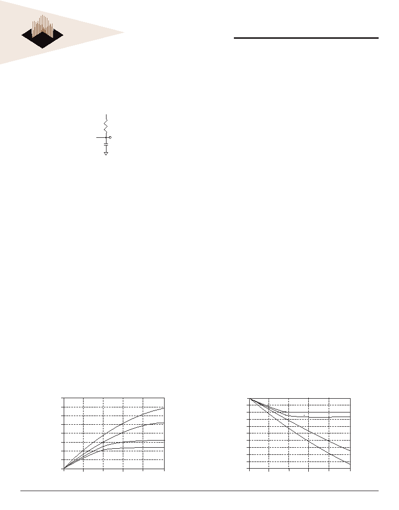
24. The I/O capacitance per DQS and DQ byte/group will not differ by more than this
maximum amount for any given device.
25. The valid data window is derived by achieving other specifi cations - t
HP
(t
CK
/2), t
DQSQ
, and
t
QH
(t
QH
= t
HP
- t
QHS
). The data valid window derates directly porportional with the clock duty
cycle and a practical data valid window can be derived. The clock is allowed a maximum
duty cycle variation of 45/55. Functionality is uncertain when operating beyond a 45/55 ratio.
The data valid window derating curves are provided below for duty cycles ranging between
50/50 and 45/55.
26. Referenced to each output group: DQS
0
with DQ
0
-DQ
7
; and DQS
1
with DQ
8
-DQ
15
of each
chip.
27. This limit is actually a nominal value and does not result in a fail value. CKE is HIGH during
REFRESH command period (t
RFC
[MIN]) else CKE is LOW (i.e., during standby).
28. To maintain a valid level, the transitioning edge of the input must:
a) Sustain a constant slew rate from the current AC level through to the target AC
level, V
IL
(AC) or V
IH
(AC).
b) Reach at least the target AC level.
c) After the AC target level is reached, continue to maintain at least the target DC
level, V
IL
(DC) or V
IH
(DC).
160
140
120
100
80
60
40
20
0
0.0
0.5 1.0 1.5 2.0 2.5
V
OUT
(V)
I
OUT
(mA)
Maximum
Nominal high
Nominal low
Minimum
FIGURE A ≠ PULL-DOWN CHARACTERISTICS
FIGURE B ≠ PULL-UP CHARACTERISTICS
0
-20
-40
-60
-80
-100
-120
-140
-160
-180
-200
0.0
0.5 1.0 1.5 2.0 2.5
V
CCQ -
V
OUT
(V)
I
OUT
(mA)
Maximum
Nominal high
Nominal low
Minimum

14
White Electronic Designs Corporation ∑ (602) 437-1520 ∑ www.wedc.com
White Electronic Designs
W3E16M72SR-XBX
February 2005
Rev. 2
29. The Input capacitance per pin group will not differ by more than this maximum
amount for any given device.
30. CK and CK# input slew rate must be
1V/ns (2V/ns differentially).
31. DQ and DM input slew rates must not deviate from DQS by more than 10%. If the
DQ/DM/DQS slew rate is less than 0.5V/ns, timing must be derated: 50ps must be
added to t
DS
and t
DH
for each 100mV/ns reduction in slew rate. If slew rate exceeds
4V/ns, functionality is uncertain.
32. V
CC
must not vary more than 4% if CKE is not active while any bank is active.
33. The clock is allowed up to ±150ps of jitter. Each timing parameter is allowed to vary
by the same amount.
34. t
HP
min is the lesser of t
CL
minimum and t
CH
minimum actually applied to the device
CK and CK# inputs, collectively during bank active.
35. READs and WRITEs with auto precharge are not allowed to be issued until
t
RAS
(MIN) can be satisfi ed prior to the internal precharge command being issued.
36. Any positive glitch must be less than 1/3 of the clock and not more than +400mV or
2.9 volts, whichever is less. Any negative glitch must be less than 1/3 of the clock
cycle and not exceed either -300mV or 2.2 volts, whichever is more positive.
37. Normal
Output
Drive
Curves:
a) The full variation in driver pull-down current from minimum to maximum
process, temperature and voltage will lie within the outer bounding lines of the
V-I curve of Figure A.
b) The variation in driver pull-down current within nominal limits of voltage and
temperature is expected, but not guaranteed, to lie within the inner bounding
lines of the V-I curve of Figure A.
c) The full variation in driver pull-up current from minimum to maximum process,
temperature and voltage will lie within the outer bounding lines of the V-I curve
of Figure B.
d) The variation in driver pull-up current within nominal limits of voltage and
temperature is expected, but not guaranteed, to lie within the inner bounding
lines of the V-I curve of Figure B.
e) The full variation in the ratio of the maximum to minimum pull-up and pull-down
current should be between .71 and 1.4, for device drain-to-source voltages from
0.1V to 1.0 Volt, and at the same voltage and temperature.
f) The full variation in the ratio of the nominal pull-up to pull-down current should be
unity ±10%, for device drain-to-source voltages from 0.1V to 1.0 Volt.
38. Reduced
Output
Drive
Curves:
a) The full variation in driver pull-down current from minimum to maximum
process, temperature and voltage will lie within the outer bounding lines of the
V-I curve of Figure C.
b) The variation in driver pull-down current within nominal limits of voltage and
temperature is expected, but not guaranteed, to lie within the inner bounding
lines of the V-I curve of Figure C.
c) The full variation in driver pull-up current from minimum to maximum process,
temperature and voltage will lie within the outer bounding lines of the V-I curve
of Figure D.
d) The variation in driver pull-up current within nominal limits of voltage and
temperature is expected, but not guaranteed, to lie within the inner bounding
lines of the V-I curve of Figure D.
e) The full variation in the ratio of the maximum to minimum pull-up and pull-down
current should be between .71 and 1.4, for device drain-to-source voltages from
0.1V to 1.0 V, and at the same voltage and temperature.
f) The full variation in the ratio of the nominal pull-up to pull-down current should be
unity ±10%, for device drain-to-source voltages from 0.1V to 1.0 V.
39. The voltage levels used are derived from a minimum V
CC
level and the referenced
test load. In practice, the voltage levels obtained from a properly terminated bus will
provide signifi cantly different voltage values.
40. V
IH
overshoot: V
IH
(MAX) = V
CCQ
+1.5V for a pulse width
3ns and the pulse width
can not be greater than 1/3 of the cycle rate.
41. V
CC
and V
CCQ
must track each other.
42. This maximum value is derived from the referenced test load. In practice, the values
obtained in a typical terminated design may refl ect up to 310ps less for t
HZ
(MAX)
and the last DVW. t
HZ
(MAX) will prevail over t
DQSCK
(MAX) + t
RPST
(MAX) condition.
t
LZ
(MIN) will prevail over t
DQSCK
(MIN) + t
RPRE
(MAX) condition.
43. For slew rates greater than 1V/ns the (LZ) transition will start about 310ps earlier.
44. During
initialization,
V
CCQ
, V
TT
, and V
REF
must be equal to or less than V
CC
+ 0.3V.
Alternatively, V
TT
may be 1.35V maximum during power up, even if V
CC
/V
CCQ
are 0
volts, provided a minimum of 42 ohms of series resistance is used between the V
TT
supply and the input pin.
45. The current part operates below the slowest JEDEC operating frequency of 83
MHz. As such, future die may not refl ect this option.
46. Reserved for future use.
47. Reserved for future use.
48. Random addressing changing 50% of data changing at every transfer.
49. Random addressing changing 100% of data changing at every transfer.
50. CKE must be active (high) during the entire time a refresh command is executed.
That is, from the time the AUTO REFRESH command is registered, CKE must be
active at each rising clock edge, until t
RFC
has been satisfi ed.
51. I
CC2N
specifi es the DQ, DQS, and DM to be driven to a valid high or low logic level.
I
CC2Q
is similar to I
CC2F
except I
CC2Q
specifi es the address and control inputs to
remain stable. Although I
CC2F
, I
CC2N
, and I
CC2Q
are similar, I
CC2F
is "worst case."
52. Whenever the operating frequency is altered, not including jitter, the DLL is required
to be reset. This is followed by 200 clock cycles before any READ command.
53. All AC timings do not count extra clock needed on address and control signals to
be registered.
54. DDR currents only. Register currents not included.
FIGURE C ≠ PULL-DOWN CHARACTERISTICS
80
70
60
50
40
30
20
10
0
0.0
0.5 1.0 1.5 2.0 2.5
V
OUT
(V)
I
OUT
(mA)
Maximum
Nominal high
Nominal low
Minimum
FIGURE D ≠ PULL-UP CHARACTERISTICS
0.0
0.5 1.0 1.5 2.0 2.5
V
CCQ -
V
OUT
(V)
I
OUT
(mA)
Maximum
Nominal high
Nominal low
Minimum
0
-10
-20
-30
-40
-50
-60
-70
-80

15
White Electronic Designs Corporation ∑ (602) 437-1520 ∑ www.wedc.com
White Electronic Designs
W3E16M72SR-XBX
February 2005
Rev. 2
ALL LINEAR DIMENSIONS ARE MILLIMETERS AND PARENTHETICALLY IN INCHES
ORDERING INFORMATION
Bottom View
32.1 (1.264) MAX
1 2 3 4 5 6 7 8 9 10 11
12
13 14
15
16
T
R
P
N
M
L
K
J
H
G
F
E
D
C
B
A
25.1 (0.988)
MAX
0.61 (0.024) NOM
2.03 (0.080) MAX
19.05 (0.750) NOM
1.27 (0.050)
NOM
19.05 (0.750)
NOM
219 X ÿ 0.762 (0.030) NOM
PACKAGE DIMENSION: 219 PLASTIC BALL GRID ARRAY (PBGA)
WHITE ELECTRONIC DESIGNS CORP.
PLASTIC DDR SDRAM
CONFIGURATION, 16M x 72
2.5V Power Supply
Registered
FREQUENCY (MHz)
200 = 200MHz
225 = 225MHz
250 = 250MHz
PACKAGE:
B = 219 Plastic Ball Grid Array (PBGA)
DEVICE GRADE:
M = Military
-55∞C to +125∞C
I = Industrial -40∞C
to
+85∞C
C = Commercial 0∞C to +70∞C
W 3E 16M 72 S R- XXX B
X

16
White Electronic Designs Corporation ∑ (602) 437-1520 ∑ www.wedc.com
White Electronic Designs
W3E16M72SR-XBX
February 2005
Rev. 2
Document Title
16M x 72 Registered DDR SDRAM Multi-Chip Package
Revision History
Rev # History
Release Date Status
Rev 0
Initial Release
August 2003
Advanced
Rev 1
Changes (Pg. 1, 15, 16)
1.1 Change mechanical drawing to new style
November 2003
Advanced
Rev 2
Changes (Pg. 1, 10, 11, 16)
2.1 Change status to Final
2.2 Update I
CC
specifi cations table values
2.3 Change max storage temperature to 125∞C
2.4
Delete V
IH
/V
IL
DC low-level input voltage operating condition
specifi cation.
2.5 Update capacitance table values
February 2005
Final