
W3E32M64S-XBX
1
White Electronic Designs Corporation ∑ (602) 437-1520 ∑ www.wedc.com
White Electronic Designs
July 2006
Rev. 3
32Mx64 DDR SDRAM
FEATURES
DDR SDRAM rate = 200, 250, 266, 333Mb/s
Package:
∑
219 Plastic Ball Grid Array (PBGA),
25mm x 25mm, 625mm
2
2.5V ±0.2V core power supply
2.5V I/O (SSTL_2 compatible)
Differential clock in puts (CK and CK#)
Commands entered on each positive CK edge
Internal pipelined double-data-rate (DDR)
ar chi tec ture; two data accesses per clock cy cle
Programmable Burst length: 2,4 or 8
Bidirectional data strobe (DQS) transmitted/
re ceived with data, i.e., source-syn chro nous data
capture (one per byte)
DQS edge-aligned with data for READs; center-
aligned with data for WRITEs
DLL to align DQ and DQS transitions with CLK
Four internal banks for concurrent operation
Data mask (DM) pins for masking write data
(one per byte)
Programmable
I
OL
/I
OH
option
Auto precharge option
Auto Refresh and Self Refresh Modes
Commercial, Industrial and Military
TemperatureRang es
Organized as 32M x 64
User
confi gurable as 2x32Mx32 or 4x32Mx16
Pinout compatible with previous W3E16M64S-XBX
version.
Weight: W3E32M64S-XBX - 2.5 grams typical
* This product subject to change without notice.
BENEFITS
41% SPACE SAVINGS vs. TSOP
Re
duced part count
Re
duced trace lengths for low er par a sit ic
ca pac i tance
Suit
able for hi-re li abil i ty ap pli ca tions
Lam
i nate in ter pos er for op ti mum TCE match
GENERAL DESCRIPTION
The 256MByte (2Gb) DDR SDRAM is a high-speed CMOS,
dy nam ic ran dom-access, memory using 4 chips containing
536,870,912 bits. Each chip is internally configured as a
quad-bank DRAM.
The 256MB DDR SDRAM uses a double data rate
ar chi tec ture to achieve high-speed operation. The
double data rate ar chi tec ture is essentially a 2n-prefetch
architecture with an in ter face designed to transfer two data
words per clock cycle at the I/O pins. A single read or write
access for the 256MB DDR SDRAM effectively consists of
a single 2n-bit wide, one-clock-cycle data transfer at the
internal DRAM core and two cor re spond ing n-bit wide,
one-half-clock-cycle data transfers at the I/O pins.
A bi-directional data strobe (DQS) is transmitted externally,
along with data, for use in data capture at the receiver.
strobe transmitted by the DDR SDRAM during READs and
by the memory controller during WRITEs. DQS is edge-
aligned with data for READs and center-aligned with data
for WRITEs. Each chip has two data strobes, one for the
lower byte and one for the upper byte.
The 256MB DDR SDRAM operates from a differential clock
(CK and CK#); the crossing of CK going HIGH and CK#
going LOW will be referred to as the positive edge of CK.
Com mands (ad dress and control signals) are registered
at every positive edge of CK. Input data is registered on
both edg es of DQS, and out put data is ref er enced to both

W3E32M64S-XBX
2
White Electronic Designs Corporation ∑ (602) 437-1520 ∑ www.wedc.com
White Electronic Designs
July 2006
Rev. 3
Area
4 x 265mm
2
= 1060mm
2
625mm
2
41%
S
A
V
I
N
G
S
Actual Size
W3E32M64S-XBX
25
White Electronic Designs
W3E32M64S-XBX
25
TSOP Approach (mm)
22.3
11.9
66
TSOP
66
TSOP
66
TSOP
66
TSOP
11.9
11.9
11.9
DENSITY COMPARISONS
edges of DQS, as well as to both edges of CK.
Read and write accesses to the DDR SDRAM are burst
ori ent ed; accesses start at a selected location and continue
for a pro grammed number of locations in a programmed
sequence. Accesses begin with the registration of an
AC TIVE command, which is then followed by a READ or
WRITE command. The address bits registered coincident
with the ACTIVE command are used to select the bank
and row to be accessed. The ad dress bits registered
coincident with the READ or WRITE com mand are used
to select the bank and the starting column location for the
burst access.
The DDR SDRAM provides for programmable READ
or WRITE burst lengths of 2, 4, or 8 locations. An auto
precharge func tion may be enabled to provide a self-
timed row precharge that is initiated at the end of the
burst access.
The pipelined, multibank architecture of DDR SDRAMs
al lows for concurrent operation, thereby providing high
ef fec tive band width by hiding row precharge and activation
time.
An auto refresh mode is provided, along with a power-
saving power-down mode.
FUNCTIONAL DE SCRIP TION
Read and write accesses to the DDR SDRAM are burst
ori ent ed; accesses start at a selected location and continue
for a pro grammed number of locations in a pro grammed
se quence. Ac cess es begin with the registration of an
AC TIVE com mand which is then followed by a READ or
WRITE com mand. The address bits registered coincident
with the AC TIVE command are used to select the bank and
row to be accessed (BA0 and BA1 select the bank, A0-12
select the row). The address bits registered coincident
with the READ or WRITE com mand are used to select the
start ing column location for the burst access.
Prior to normal operation, the DDR SDRAM must be
initialized. The following sections provide detailed
information cov er ing device initialization, register defi nition,
command de scrip tions and de vice operation.
INITIALIZATION
DDR SDRAMs must be powered up and initialized in a
pre defi ned manner. Operational procedures other than
those specifi ed may result in undefi ned operation. Power
must fi rst be applied to V
CC
and V
CCQ
simultaneously, and
then to V
REF
(and to the system V
TT
). V
TT
must be applied
after V
CCQ
to avoid device latch-up, which may cause
per ma nent dam age to the device. V
REF
can be applied any
time after V
CCQ
but is expected to be nominally coincident
with V
TT
. Except for CKE, inputs are not recognized as valid
until after V
REF
is applied. CKE is an SSTL_2 input but will

W3E32M64S-XBX
3
White Electronic Designs Corporation ∑ (602) 437-1520 ∑ www.wedc.com
White Electronic Designs
July 2006
Rev. 3
FIGURE 1 ≠ PIN CONFIGURATION
Top View
1
2
3
4
5
6
7
8
9
10
11
12
13
14
15
16
A
B
C
D
E
F
G
H
J
K
L
M
N
P
R
T
DQ15
DQ0
DQ14
DQ1
CAS0#
CS0#
V
SS
V
SS
CLK3#
NC
DQ49
DQ62
DQ48
DQ63
V
SS
V
SS
DQ31
DQ16
DQ30
DQ17
CLK1
CKE1
V
CC
V
CC
CS2#
CAS2#
DQ33
DQ46
DQ32
DQ47
V
CC
DQ13
DQ2
DQ12
DQ3
DQML0
WE0#
RAS0#
V
SS
V
SS
CKE3
CLK3
DQMH3
DQ50
DQ60
DQ51
DQ61
DQ29
DQ18
DQ28
DQ19
NC
DQMH1
CLK1#
V
CCQ
V
CCQ
RAS2#
WE2#
DQML2
DQ35
DQ44
DQ34
DQ45
DQ11
DQ4
DQ10
DQ5
V
CC
V
CC
V
CC
V
CC
V
CC
V
CC
V
CC
V
CC
DQ52
DQ57
DQ53
DQ59
DQ27
DQ20
DQ26
DQ21
V
SS
V
SS
V
SS
Vss
V
SS
V
SS
V
SS
V
SS
DQ38
DQ42
DQ36
DQ43
DQ9
DQ6
DQ8
DQ7
DQMH0
CLK0
CKE0
V
CCQ
V
CCQ
CS3#
CAS3#
WE3#
DQ54
DQ56
DQ55
DQ58
DQ25
DQ22
DQ24
DQ23
DQML1
WE1#
CS1#
V
SS
V
SS
CKE2
CLK2
DQMH2
DQ39
DQ41
DQ37
DQ40
V
SS
V
SS
V
CC
V
CCQ
DQSH3
DQSL3
CLK0#
V
SS
V
SS
NC
RAS3#
DQML3
NC
V
SS
V
CC
V
CCQ
V
CCQ
V
CC
V
SS
V
SS
V
REF
RAS1#
CAS1#
V
CC
V
CC
CLK2#
DQSL2
NC
DQSH2
V
CC
V
SS
V
SS
A9
A0
A2
A12
DQSH0
NC
NC
NC
NC
NC
A8
A1
A3
DNU
DQSL1
NC
NC
NC
NC
NC
A10
A7
A5
DNU
BA0
NC
NC
NC
NC
NC
A11
A6
A4
DNU
BA1
NC
NC
NC
NC
NC
V
SS
V
SS
V
CC
V
CCQ
DQSL0
NC
NC
V
SS
V
CC
V
CCQ
V
CCQ
V
CC
V
SS
V
SS
DQSH1
NC
NC
V
CC
V
SS
V
SS
NOTE: DNU = Do Not Use; to be left unconnected for future upgrades.
NC = Not Connected Internally.
W3E32M64S-XBX
4
White Electronic Designs Corporation ∑ (602) 437-1520 ∑ www.wedc.com
White Electronic Designs
July 2006
Rev. 3
RAS
0
#
WE
0
#
CAS
0
#
WE# RAS# CAS#
CLK
0
#
CLK#
CS
0
#
CS#
RAS
1
#
WE
1
#
CAS
1
#
WE# RAS# CAS#
CLK
1
#
CLK#
CS
1
#
CS#
A
0-12
A
0-12
BA
0-1
BA
0-1
DQ
0
DQ
15
CKE
0
CKE
DQML
0
DQML
DQMH
0
DQMH
DQ
0
DQ
15
U1
A
0-12
BA
0-1
DQ
16
DQ
31
DQ
0
DQ
15
U0
CKE
1
CKE
DQML
1
DQML
DQMH
1
DQMH
DQ
0
DQ
15
U2
A
0-12
BA
0-1
DQ
32
DQ
47
CKE
2
CKE
RAS
2
#
WE
2
#
CAS
2
#
WE# RAS# CAS#
CLK
2
#
CLK#
CS
2
#
CS#
DQML
2
DQML
DQMH
2
DQMH
RAS
3
#
WE
3
#
CAS
3
#
DQ
0
DQ
15
WE#
U3
RAS#
A
0-12
BA
0-1
CLK
3
#
CLK#
CAS#
DQ
48
DQ
63
CKE
3
CKE
CS
3
#
CS#
DQSL
3
DQSL
DQSH
3
DQSH
Y
=
Y
=
Y
=
Y
=
Y
=
Y
=
Y
=
Y
=
Y
=
Y
=
Y
=
Y
=
Y
=
Y
=
Y
=
Y
=
Y
=
Y
=
Y
=
Y
=
Y
=
Y
=
Y
=
Y
=
Y
=
Y
=
Y
=
Y
=
Y
=
Y
=
Y
=
Y
=
Y
=
Y
=
Y
=
Y
=
Y
=
Y
=
Y
=
Y
=
Y
=
Y
=
Y
=
Y
=
Y
=
Y
=
Y
=
Y
=
CLK
3
CLK
V
REF
DQSL
2
DQSL
DQSH
2
DQSH
V
REF
DQSL
1
DQSL
DQSH
1
DQSH
V
REF
DQSL
0
DQSL
DQSH
0
DQSH
CLK
2
CLK
CLK
1
CLK
CLK
0
CLK
V
REF
DQML
3
DQML
DQMH
3
DQMH
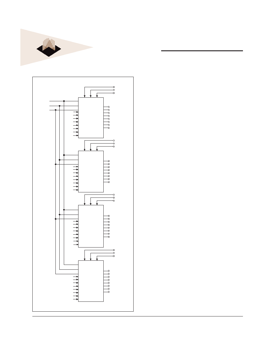
FIGURE 2 ≠ FUNCTIONAL BLOCK DIAGRAM
detect an L
VCMOS
LOW level after V
CC
is applied. After CKE
passes through V
IH
, it will transition to an SSTL_2 signal
and remain as such until power is cycled. Maintaining an
L
VCMOS
LOW level on CKE during power-up is required
to ensure that the DQ and DQS outputs will be in the
High-Z state, where they will remain until driven in normal
operation (by a read ac cess). After all power supply and
reference voltages are stable, and the clock is stable, the
DDR SDRAM requires a 200µs delay prior to applying an
executable com mand.
Once the 200µs delay has been satisfi ed, a DESELECT
or NOP command should be applied, and CKE should
be brought HIGH. Following the NOP command, a
PRECHARGE ALL command should be applied. Next a
LOAD MODE REG IS TER command should be issued for
the extended mode register (BA1 LOW and BA0 HIGH)
to enable the DLL, fol lowed by another LOAD MODE
REGISTER command to the mode register (BA0/BA1
both LOW) to reset the DLL and to program the operating
parameters. Two-hundred clock cy cles are required
between the DLL reset and any READ command. A
PRECHARGE ALL command should then be applied,
placing the device in the all banks idle state.
Once in the idle state, two AUTO REFRESH cycles must
be performed (t
RFC
must be satisfi ed.) Additionally, a LOAD
MODE REGISTER command for the mode register with
the reset DLL bit deactivated (i.e., to program operating
pa ram e ters without resetting the DLL) is required.
Following these requirements, the DDR SDRAM is ready
for normal op er a tion.

W3E32M64S-XBX
5
White Electronic Designs Corporation ∑ (602) 437-1520 ∑ www.wedc.com
White Electronic Designs
July 2006
Rev. 3
REGISTER DEFINITION
MODE REGISTER
The Mode Register is used to defi ne the specifi c mode of
op er a tion of the DDR SDRAM. This defi nition includes the
selection of a burst length, a burst type, a CAS latency,
and an op er at ing mode, as shown in Figure 3. The Mode
Reg is ter is programmed via the MODE REG IS TER SET
command (with BA0 = 0 and BA1 = 0) and will retain
the stored in for ma tion until it is pro grammed again or
the device loses power. (Ex cept for bit A8 which is self
clearing).
Reprogramming the mode register will not alter the contents
of the memory, provided it is performed correctly. The Mode
Reg is ter must be load ed (reloaded) when all banks are
idle and no bursts are in progress, and the con trol ler must
wait the spec i fi ed time be fore ini ti at ing the sub se quent
op er a tion. Vi o lat ing either of these re quire ments will result
in un spec i fi ed operation.
Mode register bits A0-A2 specify the burst length, A3 spec i fi es
the type of burst (sequential or in ter leaved), A4-A6 spec i fy the
CAS latency, and A7-A12 specify the op er at ing mode.
BURST LENGTH
Read and write ac cess es to the DDR SDRAM are burst
ori ent ed, with the burst length being programmable,
as shown in Fig ure 3. The burst length determines
the maximum num ber of column lo ca tions that can be
accessed for a given READ or WRITE command. Burst
lengths of 2, 4 or 8 lo ca tions are avail able for both the
sequential and the in ter leaved burst types.
Reserved states should not be used, as unknown op er a tion
or incompatibility with future versions may result.
When a READ or WRITE command is issued, a block of
col umns equal to the burst length is effectively selected.
All accesses for that burst take place within this block,
mean ing that the burst will wrap within the block if a
boundary is reached. The block is uniquely selected by
A1-Ai when the burst length is set to two; by A2-Ai when the
burst length is set to four (where Ai is the most signifi cant
column address for a given confi guration); and by A3-Ai
when the burst length is set to eight. The remaining (least
sig nifi cant) ad dress bit(s) is (are) used to select the starting
lo ca tion within the block. The pro grammed burst length
ap plies to both READ and WRITE bursts.
BURST TYPE
Accesses within a given burst may be pro grammed to be
either se quen tial or interleaved; this is re ferred to as the
burst type and is selected via bit M3.
The ordering of accesses within a burst is de ter mined by
the burst length, the burst type and the start ing column
address, as shown in Table 1.
READ LATENCY
The READ latency is the delay, in clock cycles, between
the reg is tra tion of a READ command and the avail abil i ty
of the fi rst bit of output data. The latency can be set to 2
or 2.5 clocks.
If a READ command is registered at clock edge n, and the
latency is m clocks, the data will be available by clock edge
n+m. Table 2 below indicates the op er at ing fre quen cies at
which each CAS latency setting can be used.
Reserved states should not be used as unknown operation
or incompatibility with future versions may result.
OPERATING MODE
The normal operating mode is selected by issuing a MODE
REGISTER SET command with bits A7-A12 each set to
zero, and bits A0-A6 set to the desired values. A DLL reset
is initiated by issuing a MODE REGISTER SET command
with bits A7 and A9-A12 each set to zero, bit A8 set to one,
and bits A0-A6 set to the desired values. Although not
re quired, JEDEC specifi cations recommend when a LOAD
MODE REG IS TER command is issued to reset the DLL, it
should always be followed by a LOAD MODE REGISTER
command to se lect nor mal op er at ing mode.
All other combinations of values for A7-A12 are reserved
for future use and/or test modes. Test modes and reserved
states should not be used because unknown operation or
incompatibility with future versions may result.
EXTENDED MODE REGISTER
The extended mode register controls functions beyond
those controlled by the mode register; these additional
functions are DLL enable/disable, output drive strength,