W3EG72255S-D3
-JD3
-AJD3
1
White Electronic Designs
November 2004
Rev. 2
PRELIMINARY*
White Electronic Designs Corporation ∑ (602) 437-1520 ∑ www.wedc.com
FEATURES
Double-data-rate architecture
DDR200, DDR266 and DDR333:
∑ JEDEC design specifi cations
Bi-directional data strobes (DQS)
Differential clock inputs (CK & CK#)
Programmable Read Latency 2,2.5 (clock)
Programmable Burst Length (2,4,8)
Programmable Burst type (sequential & interleave)
Edge aligned data output, center aligned data input.
Auto and self refresh
Serial presence detect
Dual
Rank
Power supply: V
CC =
2.5V ± 0.2V
JEDEC standard 184 pin DIMM package
∑ Package height options:
JD3: 30.48mm (1.2"),
AJD3: 28.70mm (1.13")
NOTE: Consult factory for availability of:
∑ RoHS compliant products
∑ Vendor source control options
∑ Industrial temperature option
DESCRIPTION
The W3EG72255S is a 2x128Mx72 Double Data Rate
SDRAM memory module based on 512Mb DDR SDRAM
components. The module consists of eighteen 256Mx4
stacks, in 66 pin TSOP packages mounted on a 184 pin
FR4 substrate.
Synchronous design allows precise cycle control with the
use of system clock. Data I/O transactions are possible
on both edges and Burst Lengths allow the same
device to be useful for a variety of high bandwidth, high
performance memory system applications.
* wThis product is under development, is not qualifi ed or characterized and is subject
to change without notice.
PRELIMINARY*
2GB ≠ 2x128Mx72 DDR SDRAM REGISTERED ECC, w/PLL
OPERATING FREQUENCIES
DDR333 @CL=2.5
DDR266 @CL=2
DDR266 @CL=2
DDR266 @CL=2.5
DDR200 @CL=2
Clock Speed
166MHz
133MHz
133MHz
133MHz
100MHz
CL-t
RCD
-t
RP
2.5-3-3
2-2-2
2-3-3
2.5-3-3
2-2-2
W3EG72255S-D3
-JD3
-AJD3
2
White Electronic Designs
November 2004
Rev. 2
PRELIMINARY
White Electronic Designs Corporation ∑ (602) 437-1520 ∑ www.wedc.com
PIN
SYMBOL
PIN
SYMBOL
PIN
SYMBOL
PIN
SYMBOL
1
V
REF
47
DQS8
93
V
SS
139
V
SS
2
DQ0
48
A0
94
DQ4
140
DQS17
3
V
SS
49
CB2
95
DQ5
141
A10
4
DQ1
50
V
SS
96
V
CCQ
142
CB6
5
DQS0
51
CB3
97
DQS9
143
V
CCQ
6
DQ2
52
BA1
98
DQ6
144
CB7
7
V
CC
53
DQ32
99
DQ7
145
V
SS
8
DQ3
54
V
CCQ
100
V
SS
146
DQ36
9
NC
55
DQ33
101
NC
147
DQ37
10
RESET#
56
DQS4
102
NC
148
V
CC
11
V
SS
57
DQ34
103
NC
149
DQS13
12
DQ8
58
V
SS
104
V
CCQ
150
DQ38
13
DQ9
59
BA0
105
DQ12
151
DQ39
14
DQS1
60
DQ35
106
DQ13
152
V
SS
15
V
CCQ
61
DQ40
107
DQS10
153
DQ44
16
NC
62
V
CCQ
108
V
CC
154
RAS#
17
NC
63
WE#
109
DQ14
155
DQ45
18
V
SS
64
DQ41
110
DQ15
156
V
CCQ
19
DQ10
65
CAS#
111
CKE1
157
CS0#
20
DQ11
66
V
SS
112
V
CCQ
158
CS1#
21
CKE0
67
DQS5
113
NC
159
DQS14
22
V
CCQ
68
DQ42
114
DQ20
160
V
SS
23
DQ16
69
DQ43
115
A12
161
DQ46
24
DQ17
70
V
CC
116
V
SS
162
DQ47
25
DQS2
71
NC
117
DQ21
163
NC
26
V
SS
72
DQ48
118
A11
164
V
CCQ
27
A9
73
DQ49
119
DQS11
165
DQ52
28
DQ18
74
V
SS
120
V
CC
166
DQ53
29
A7
75
NC
121
DQ22
167
NC
30
V
CCQ
76
NC
122
A8
168
V
CC
31
DQ19
77
V
CCQ
123
DQ23
169
DQS15
32
A5
78
DQS6
124
V
SS
170
DQ54
33
DQ24
79
DQ50
125
A6
171
DQ55
34
V
SS
80
DQ51
126
DQ28
172
V
CCQ
35
DQ25
81
V
SS
127
DQ29
173
NC
36
DQS3
82
V
CCID
128
V
CCQ
174
DQ60
37
A4
83
DQ56
129
DQS12
175
DQ61
38
V
CC
84
DQ57
130
A3
176
V
SS
39
DQ26
85
V
CC
131
DQ30
177
DQS16
40
DQ27
86
DQS7
132
V
SS
178
DQ62
41
A2
87
DQ58
133
DQ31
179
DQ63
42
V
SS
88
DQ59
134
CB4
180
V
CCQ
43
A1
89
V
SS
135
CB5
181
SA0
44
CB0
90
NC
136
V
CCQ
182
SA1
45
CB1
91
SDA
137
CK0
183
SA2
46
V
CC
92
SCL
138
CK0#
184
V
CCSPD
PIN CONFIGURATION
A0-A12
Address input (Multiplexed)
BA0-BA1
Bank Select Address
DQ0-DQ63
Data Input/Output
CB0-CB7
Check bits
DQS0-DQS17
Data Strobe Input/Output
CK0
Clock Input
CK0#
Clock Input
CKE0, CKE1
Clock Enable input
CS0#, CS1#
Chip Select Input
RAS#
Row Address Strobe
CAS#
Column Address Strobe
WE#
Write Enable
V
CC
Power Supply
V
CCQ
Power Supply for DQS
V
SS
Ground
V
REF
Power Supply for Reference
V
CCSPD
Serial EEPROM Power Supply
SDA
Serial data I/O
SCL
Serial clock
SA0-SA2
Address in EEPROM
V
CCID
V
CC
Indentifi cation Flag
NC
No Connect
RESET#
Reset Enable
PIN NAMES

W3EG72255S-D3
-JD3
-AJD3
3
White Electronic Designs
November 2004
Rev. 2
PRELIMINARY
White Electronic Designs Corporation ∑ (602) 437-1520 ∑ www.wedc.com
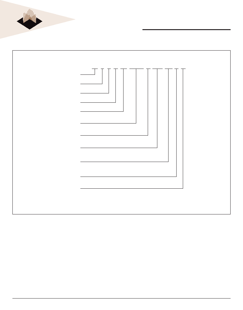
FUNCTIONAL BLOCK DIAGRAM
DQS2
DQS1
DQS0
DQS7
DQS6
DQS5
DQS4
DQS3
DQS12
DQ60
DQ56
I/O 3
DQ59
DQ58
DQ57
I/O 1
I/O 0
I/O 2
DQ63
DQ62
DQ61
DQ51
DQ50
DQ49
DQ48
DQ43
DQ42
DQ41
DQ40
DQS
DM
CS#
DQS
DM
CS#
DQS
DM
CS#
I/O 1
I/O 0
I/O 3
I/O 2
I/O 1
I/O 0
I/O 3
I/O 2
DQ35
DQ34
DQ33
DQ32
DQ27
DQ26
DQ25
DQ24
DQS
DM
CS#
DQS
DM
CS#
I/O 1
I/O 0
I/O 3
I/O 2
I/O 1
I/O 0
I/O 3
I/O 2
DQS14
DQS15
DQS16
DQ55
DQ54
DQ53
DQ52
DQ47
DQ46
DQ45
DQ44
DQS13
DQ39
DQ38
DQ37
DQ36
DQ31
DQ30
DQ29
DQ28
I/O 3
I/O 2
I/O 0
I/O 1
DM
DM
DM
DM
DM
I/O 2
I/O 3
I/O 0
I/O 1
I/O 2
I/O 3
I/O 0
I/O 1
DQS
DQS
DQS
I/O 2
I/O 3
I/O 0
I/O 1
I/O 2
I/O 3
I/O 0
I/O 1
DQS
DQS
DQ2
I/O 1
DQ18
DQ16
DQ17
DQ19
DQ11
DQ10
DQ9
DQ8
DQ3
DQS
DM
CS#
DQS
DM
CS#
I/O 0
I/O 1
I/O 0
I/O 3
I/O 2
I/O 1
I/O 0
I/O 3
I/O 2
DQ1
DQ0
CS#
DM
DQS
I/O 2
I/O 3
DQ6
DQS10
DQS11
DQ7
DQ20
DQ21
DQ22
DQ23
DQ15
DQ14
DQ13
DQ12
DQ1
DQ2
DQS9
DQ5
DQ4
DM
DM
DM
CS#
CS#
CS#
CS#
CS#
CS#
CS#
CS#
CS#
CS#
CS#
CS#
CS#
CS#
CS#
CS#
CS#
CS#
I/O 1
I/O 2
I/O 3
I/O 0
I/O 1
I/O 2
I/O 3
I/O 0
I/O 1
I/O 0
DQS
DQS
I/O 3
I/O 2
DQS
RCS0#
RCS1#
I/O 3
I/O 2
DQS
DM
CS#
I/O 0
I/O 1
CS#
DM
DQS
CS#
DM
DQS
CS#
DM
DQS
CS#
DM
DQS
CS#
DM
DQS
CS#
DM
DQS
CS#
DM
DQS
I/O 2
I/O 3
I/O 0
I/O 1
I/O 2
I/O 3
I/O 0
I/O 1
I/O 2
I/O 3
I/O 0
I/O 1
I/O 2
I/O 3
I/O 0
I/O 1
I/O 2
I/O 3
I/O 0
I/O 1
I/O 2
I/O 0
I/O 1
I/O 3
I/O 2
I/O 0
I/O 1
I/O 3
DM
DM
DM
DM
DM
DM
DM
DM
DQS
I/O 1
I/O 0
I/O 2
I/O 3
I/O 2
I/O 1
I/O 0
DQS
I/O 3
DQS
I/O 1
I/O 0
I/O 3
I/O 2
DQS
I/O 1
I/O 0
I/O 3
I/O 2
DQS
I/O 3
I/O 1
I/O 0
I/O 2
I/O 1
I/O 0
I/O 3
I/O 2
DQS
DQS
I/O 1
I/O 0
I/O 3
I/O 2
DQS
I/O 2
I/O 3
I/O 1
I/O 0
V
SS
DQS8
CS#
DM
DQS
I/O 2
I/O 0
I/O 1
CB1
CB2
CB3
I/O 3
CB0
I/O 3
I/O 1
I/O 0
I/O 2
DQS
DM
CS#
DQS17
I/O 3
I/O 2
I/O 0
I/O 1
DQS
DQS
DM
I/O 1
I/O 0
I/O 2
I/O 3
CB5
CB6
CB7
CB4
DM
RCS0#
RRAS#
RA0-RA12
RCKE0
RCAS#
RBA0,RBA1
RCS1#
RESET#
PCK#
PCK
A0-A12
WE#
CAS#
RAS#
BA0,BA1
CS0#
CKE0
R
E
I
G
E
R
T
S
RCKE1
RWE#
BA0,BA1: DDR SDRAMs
A0-A12: DDR SDRAMs
RAS#: DDR SDRAMs
CAS#: DDR SDRAMs
WE#: DDR SDRAMs
CKE: DDR SDRAMs
CKE: DDR SDRAMs
CS1#
CKE1
A0
SA0
WP
SCL
A1
A2
SA1
SA2
SDA
SERIAL PD
PLL
CK0
CK0#
REGISTER
SDRAM
V
SS
V
REF
V
CC
/V
CCQ
V
CCSPD
DDR SDRAMs
SPD
DDR SDRAMs
DDR SDRAMs
Notes:
1.
DQ-to-I/O wiring is shown as recommended but may be changed.
2.
DQ/DQS/DM/CKE/S relationships must be maintained as shown.
NOTE: All resistor values are 22 ohms unless otherwise specifi ed
W3EG72255S-D3
-JD3
-AJD3
4
White Electronic Designs
November 2004
Rev. 2
PRELIMINARY
White Electronic Designs Corporation ∑ (602) 437-1520 ∑ www.wedc.com
Parameter
Symbol
Value
Units
Voltage on any pin relative to V
SS
V
IN
, V
OUT
-0.5 - 3.6
V
Voltage on V
CC
supply relative to V
SS
V
CC
, V
CCQ
-1.0 - 3.6
V
Storage Temperature
T
STG
-55 - +150
∞C
Power Dissipation
P
D
27
W
Short Circuit Current
I
0S
50
mA
Note: Permanent device damage may occur if `ABSOLUTE MAXIMUM RATINGS' are exceeded.
Functional operation should be restricted to recommended operating condition.
Exposure to higher than recommended voltage for extended periods of time could affect device reliability
ABSOLUTE MAXIMUM RATINGS
Parameter
Symbol
Min
Max
Unit
Supply Voltage
V
CC
2.3
2.7
V
Supply Voltage
V
CCQ
2.3
2.7
V
Reference Voltage
V
REF
1.15
1.35
V
Termination Voltage
V
TT
1.15
1.35
V
Input High Voltage
V
IH
V
REF
+ 0.15
V
CCQ
+ 0.3
V
Input Low Voltage
V
IL
-0.3
V
REF
- 0.15
V
Output High Voltage
V
OH
V
TT
+ 0.76
--
V
Output Low Voltage
V
OL
--
V
TT
- 0.76
V
Parameter
Symbol
Max
Unit
Input Capacitance (A0-A12)
C
IN1
6.25
pF
Input Capacitance (RAS#, CAS#, WE#)
C
IN2
6.25
pF
Input Capacitance (CKE0)
C
IN3
6.25
pF
Input Capacitance (CK0,CK0#)
C
IN4
5.5
pF
Input Capacitance (CS0#)
C
IN5
6.25
pF
Input Capacitance (DQM0-DQM8)
C
IN6
13.0
pF
Input Capacitance (BA0-BA1)
C
IN7
6.25
pF
Data input/output capacitance (DQ0-DQ63)(DQS)
C
OUT
13.0
pF
Data input/output capacitance (CB0-CB7)
C
OUT
13.0
pF
DC CHARACTERISTICS
0∞C
T
A
70∞C, V
CC
= 2.5V ± 0.2V
CAPACITANCE
T
A
= 25∞C, f = 1MHz, V
CC
= 2.5V ± 0.2V
W3EG72255S-D3
-JD3
-AJD3
5
White Electronic Designs
November 2004
Rev. 2
PRELIMINARY
White Electronic Designs Corporation ∑ (602) 437-1520 ∑ www.wedc.com
I
DD
SPECIFICATIONS AND TEST CONDITIONS
0∞C
T
A
+70∞C, V
CCQ
= 2.5V ± 0.2V, V
CC
= 2.5V ± 0.2V.
Includes DDR SDRAM components only
Parameter
Symbol
Rank 1
Conditions
DDR333@CL=2.5
Max
DDR266:@CL=2, 2.5
Max
DDR200@CL=2
Max
Units
Rank 2
Standby
State
Operating Current
I
DD0
One device bank; Active - Precharge; t
RC
= t
RC
(MIN); t
CK
= t
CK
(MIN); DQ,DM and
DQS inputs changing once per clock cycle;
Address and control inputs changing once
every two cycles.
4140
4140
4140
mA
I
DD3N
Operating Current
I
DD1
One device bank; Active-Read-Precharge
Burst = 2; t
RC
= t
RC
(MIN); t
CK
= t
CK
(MIN);
l
OUT
= 0mA; Address and control inputs
changing once per clock cycle.
4680
4680
4680
mA
I
DD3N
Precharge Power-
Down Standby Current
I
DD2P
All device banks idle; Power-down mode;
t
CK
= t
CK
(MIN); CKE = (low)
180
180
180
rnA
I
DD2P
Idle Standby Current
I
DD2F
CS# = High; All device banks idle;
t
CK
= t
CK
(MIN); CKE = High; Address
and other control inputs changing once
per clock cycle. V
IN
= V
REF
for DQ, DQS
and DM.
1620
1620
1620
mA
I
DD2F
Active Power-Down
Standby Current
I
DD3P
One device bank active; Power-Down
mode; t
CK
(MIN); CKE = (low)
1260
1260
1260
mA
I
DD3P
Active Standby Current
I
DD3N
CS# = High; CKE = High; One device
bank; Active-Precharge;t
RC
= t
RAS
(MAX);
t
CK
= t
CK
(MIN); DQ, DM and DQS inputs
changing twice per clock cycle; Address
and other control inputs changing once per
clock cycle.
1800
1800
1800
mA
I
DD3N
Operating Current
I
DD4R
Burst = 2; Reads; Continuous burst; One
device bank active; Address and control
inputs changing once per clock cycle; t
CK
=
t
CK
(MIN); l
OUT
= 0mA.
4770
4770
4770
mA
I
DD3N
Operating Current
I
DD4W
Burst = 2; Writes; Continuous burst; One
device bank active; Address and control
inputs changing once per clock cycle;
t
CK
= t
CK
(MIN); DQ,DM and DQS inputs
changing once per clock cycle.
4590
4590
4590
rnA
I
DD3N
Auto Refresh Current
I
DD5
t
RC
= t
RC
(MIN)
7020
7020
7020
mA
I
DD3N
Self Refresh Current
I
DD6
CKE
0.2V
180
180
180
mA
I
DD6
Operating Current
I
DD7A
Four bank interleaving Reads (BL=4)
with auto precharge with t
RC
=t
RC
(MIN);
t
CK
=t
CK
(MIN); Address and control inputs
change only during Active Read or Write
commands.
9090
9000
9000
mA
I
DD3N
W3EG72255S-D3
-JD3
-AJD3
6
White Electronic Designs
November 2004
Rev. 2
PRELIMINARY
White Electronic Designs Corporation ∑ (602) 437-1520 ∑ www.wedc.com
I
DD
SPECIFICATIONS AND TEST CONDITIONS
0∞C
T
A
+70∞C, V
CCQ
= 2.5V ± 0.2V, V
CC
= 2.5V ± 0.2V.
Includes PLL and register power
Parameter
Symbol
Rank 1
Conditions
DDR333@CL=2.5
Max
DDR266:@CL=2, 2.5
Max
DDR200@CL=2
Max
Units
Rank 2
Standby
State
Operating Current
I
DD0
One device bank; Active - Precharge;
t
RC
= t
RC
(MIN); t
CK
= t
CK
(MIN); DQ,DM
and DQS inputs changing once per
clock cycle; Address and control inputs
changing once every two cycles.
4725
4725
4725
mA
I
DD3N
Operating Current
I
DD1
One device bank; Active-Read-
Precharge Burst = 2; t
RC
= t
RC
(MIN);
t
CK
= t
CK
(MIN); l
OUT
= 0mA; Address
and control inputs changing once per
clock cycle.
5265
5265
5265
mA
I
DD3N
Precharge Power-
Down Standby Current
I
DD2P
All device banks idle; Power-down mode;
t
CK
= t
CK
(MIN); CKE = (low)
180
180
180
rnA
I
DD2P
Idle Standby Current
I
DD2F
CS# = High; All device banks idle;
t
CK
= t
CK
(MIN); CKE = High; Address
and other control inputs changing once
per clock cycle. V
IN
= V
REF
for DQ, DQS
and DM.
1930
1930
1930
mA
I
DD2F
Active Power-Down Standby
Current
I
DD3P
One device bank active; Power-Down
mode; t
CK
(MIN); CKE = (low)
1260
1260
1260
mA
I
DD3P
Active Standby Current
I
DD3N
CS# = High; CKE = High; One device
bank; Active-Precharge;t
RC
= t
RAS
(MAX);
t
CK
= t
CK
(MIN); DQ, DM and DQS inputs
changing twice per clock cycle; Address
and other control inputs changing once
per clock cycle.
2110
2110
2110
mA
I
DD3N
Operating Current
I
DD4R
Burst = 2; Reads; Continuous burst; One
device bank active; Address and control
inputs changing once per clock cycle; t
CK
= t
CK
(MIN); l
OUT
= 0mA.
5355
5355
5355
mA
I
DD3N
Operating Current
I
DD4W
Burst = 2; Writes; Continuous burst; One
device bank active; Address and control
inputs changing once per clock cycle;
t
CK
= t
CK
(MIN); DQ,DM and DQS inputs
changing once per clock cycle.
5535
5175
5175
rnA
I
DD3N
Auto Refresh Current
I
DD5
t
RC
= t
RC
(MIN)
7640
7640
7640
mA
I
DD3N
Self Refresh Current
I
DD6
CKE
0.2V
455
455
455
mA
I
DD6
Operating Current
I
DD7A
Four bank interleaving Reads (BL=4)
with auto precharge with t
RC
=t
RC
(MIN);
t
CK
=t
CK
(MIN); Address and control inputs
change only during Active Read or Write
commands.
9675
9585
9585
mA
I
DD3N

W3EG72255S-D3
-JD3
-AJD3
7
White Electronic Designs
November 2004
Rev. 2
PRELIMINARY
White Electronic Designs Corporation ∑ (602) 437-1520 ∑ www.wedc.com
I
DD1
: OPERATING CURRENT: ONE BANK
1. Typical Case: V
CC
= 2.5V, T = 25∞C
2. Worst Case: V
CC
= 2.7V, T = 10∞C
3. Only one bank is accessed with t
RC
(min), Burst
Mode, Address and Control inputs on NOP edge are
changing once per clock cycle. l
OUT
= 0mA
4. Timing patterns
∑ DDR200 (100MHz, CL = 2) : t
CK
= 10ns, CL2, BL =
4, t
RCD
= 2*t
CK
, t
RAg
= 5*t
CK
Read: A0 N R0 N N P0 N A0 N - repeat the same
timing with random address changing; 50% of data
changing at every burst
∑ DDR266 (133MHz, CL = 2.5) : t
CK
= 7.5ns, CL =
2.5, BL = 4, t
RCD
= 3*t
CK
, t
RC
= 9*t
CK
, t
RAg
= 5*t
CK
Read: A0 N N R0 N P0 N N N A0 N - repeat the
same timing with random address changing; 50% of
data changing at every burst
∑ DDR266 (133MHz, CL = 2) : t
CK
= 7.5ns, CL = 2, BL
= 4, t
RCD
= 3*t
CK
, t
RC
= 9*t
CK
, t
RAg
= 5*t
CK
Read: A0 N N R0 N P0 N N N A0 N - repeat the
same timing with random address changing; 50% of
data changing at every burst
∑ DDR333 (166MHz, CL = 2.5) : t
CK
= 6ns, BL = 4,
t
RCD
= 10*t
CK
, t
RAg
= 7*t
CK
Read: A0 N N R0 N P0 N N N A0 N -- repeat the
same timing with random address changing; 50% of
data changing at every burst
I
DD7A
: OPERATING CURRENT: FOUR BANKS
1. Typical Case: V
CC
= 2.5V, T = 25∞C
2. Worst Case: V
CC
= 2.7V, T = 10∞C
3. Four banks are being interleaved with t
RC
(min), Burst
Mode, Address and Control inputs on NOP edge are
not changing.
lout = 0mA
4. Timing patterns
∑ DDR200 (100MHz, CL = 2) : t
CK
= 10ns, CL2,
BL = 4, t
RRD
= 2*t
CK
, t
RCD
= 3*t
CK
, Read with
autoprecharge
Read: A0 N A1 R0 A2 R1 A3 R2 A0 R3 A1 R0
- repeat the same timing with random address
changing; 100% of data changing at every burst
∑ DDR266 (133MHz, CL = 2.5) : t
CK
= 7.5ns, CL =
2.5, BL = 4, t
RRD
= 3*t
CK
, t
RCD
= 3*t
CK
Read with
autoprecharge
Read: A0 N A1 R0 A2 R1 A3 R2 N R3 A0 N A1
R0 - repeat the same timing with random address
changing; 100% of data changing at every burst
∑ DDR266 (133MHz, CL = 2): t
CK
= 7.5ns, CL2 = 2,
BL = 4, t
RRD
= 2*t
CK
, t
RCD
= 3*t
CK
Read: A0 N A1 R0 A2 R1 A3 R2 N R3 A0 N A1
R0 - repeat the same timing with random address
changing; 100% of data changing at every burst
∑ DDR333 (166MHz, CL = 2.5) : t
CK
= 6ns, BL = 4,
t
RRD
= 3*t
CK
, t
RCD
= 3*t
CK
, Read with autoprecharge
Read: A0 N A1 R0 A2 R1 A3 R2 N R3 A0 N A1
R0 - repeat the same timing with random address
changing; 100% of data changing at every burst
Legend: A = Activate, R = Read, W = Write, P =
DETAILED TEST CONDITIONS FOR DDR SDRAM I
DD1
& I
DD7A
Precharge, N = NOP
A (0-3) = Activate Bank 0-3
R (0-3) = Read Bank 0-3
W3EG72255S-D3
-JD3
-AJD3
8
White Electronic Designs
November 2004
Rev. 2
PRELIMINARY
White Electronic Designs Corporation ∑ (602) 437-1520 ∑ www.wedc.com
DDR SDRAM COMPONENT ELECTRICAL CHARACTERISTICS AND
RECOMMENDED AC OPERATING CONDITIONS
0∞C T
A
+70∞C; V
CC
= +2.5V ±0.2V, V
CCQ
= +2.5V ±0.2V
AC Characteristics
335
262/263/265
202
Parameter
Symbol
Min
Max
Min
Max
Min
Max
Units
Notes
Access window of DQs from CK, CK#
t
AC
-0.7
+0.7
-0.75
+0.75
-0.8
+0.8
ns
CK high-level width
t
CH
0.45
0.55
0.45
0.55
0.45
0.55
t
CK
16
CK low-level width
t
CL
0.45
0.55
0.45
0.55
0.45
0.55
t
CK
16
Clock cycle time
CL=2.5
t
CK
(2.5)
6
13
7.5
13
8
13
ns
22
CL=2
t
CK
(2)
7.5
13
7.5
13
10
13
ns
22
DQ and DM input hold time relative to DQS
t
DH
0.45
0.5
0.6
ns
14,17
DQ and DM input setup time relative to DQS
t
DS
0.45
0.5
0.6
ns
14,17
DQ and DM input pulse width (for each input)
t
DIPW
1.75
1.75
2
ns
17
Access window of DQS from CK, CK#
t
DQSCK
-0.60
+0.60
-0.75
+0.75
-0.8
+0.8
ns
DQS input high pulse width
t
DQSH
0.35
0.35
0.35
t
CK
DQS input low pulse width
t
DQSL
0.35
0.35
0.35
t
CK
DQS-DQ skew, DQS to last DQ valid, per group, per access
t
DQSQ
0.45
0.5
0.5
ns
13,14
Write command to fi rst DQS latching transition
t
DQSS
0.75
1.25
0.75
1.25
0.75
1.25
t
CK
DQS falling edge to CK rising - setup time
t
DSS
0.2
0.2
0.2
t
CK
DQS falling edge from CK rising - hold time
t
DSH
0.2
0.2
0.2
t
CK
Half clock period
t
HP
t
CH
, t
CL
t
CH
, t
CL
t
CH
, t
CL
ns
18
Data-out high-impedance window from CK, CK#
t
HZ
+0.70
+0.75
+0.8
ns
8,19
Data-out low-impedance window from CK, CK#
t
LZ
-0.70
-0.75
-0.8
ns
8,20
Address and control input hold time (fast slew rate)
t
IHf
0.75
0.90
1.1
ns
6
Address and control input set-up time (fast slew rate)
t
ISf
0.75
0.90
1.1
ns
6
Address and control input hold time (slow slew rate)
t
IHs
0.80
1
1.1
ns
6
Address and control input setup time (slow slew rate)
t
ISs
0.80
1
1.1
ns
6
Address and control input pulse width (for each input)
t
IPW
2.2
2.2
2.2
ns
LOAD MODE REGISTER command cycle time
t
MRD
12
15
16
ns
DQ-DQS hold, DQS to fi rst DQ to go non-valid, per access
t
QH
t
HP
-t
QHS
t
HP
-t
QHS
t
HP
-t
QHS
ns
13,14
Data hold skew factor
t
QHS
0.55
0.75
.75
ns
ACTIVE to PRECHARGE command
t
RAS
42
70,000
40
120,000
40
120,000
ns
15
ACTIVE to READ with Auto precharge command
t
RAP
15
15
15
ns
ACTIVE to ACTIVE/AUTO REFRESH command period
t
RC
60
65
70
ns
AUTO REFRESH command period
t
RFC
72
75
75
ns
21
W3EG72255S-D3
-JD3
-AJD3
9
White Electronic Designs
November 2004
Rev. 2
PRELIMINARY
White Electronic Designs Corporation ∑ (602) 437-1520 ∑ www.wedc.com
DDR SDRAM COMPONENT ELECTRICAL CHARACTERISTICS AND
RECOMMENDED AC OPERATING CONDITIONS (continued)
0∞C T
A
+70∞C; V
CC
= +2.5V ±0.2V, V
CCQ
= +2.5V ±0.2V
AC Characteristics
335
262/263/265
202
Parameter
Symbol
Min
Max
Min
Max
Min
Max
Units
Notes
ACTIVE to READ or WRITE delay
t
RCD
15
15
15
ns
PRECHARGE command period
t
RP
15
15
15
ns
DQS read preamble
t
RPRE
0.9
1.1
0.9
1.1
0.9
1.1
t
CK
19
DQS read postamble
t
RPST
0.4
0.6
0.4
0.6
0.4
0.6
t
CK
ACTIVE bank a to ACTIVE bank b command
t
RRD
12
15
15
ns
DQS write preamble
t
WPRE
0.25
0.25
0.25
t
CK
DQS write preamble setup time
t
WPRES
0
0
0
ns
10,11
DQS write postamble
t
WPST
0.4
0.6
0.4
0.6
0.4
0.6
t
CK
9
Write recovery time
t
WR
15
15
15
ns
Internal WRITE to READ command delay
t
WTR
1
1
1
t
CK
Data valid output window
NA
t
QH
-t
DQSQ
t
QH
-t
DQSQ
t
QH
-t
DQSQ
ns
13
REFRESH to REFRESH command interval
t
REFC
70.3
70.3
70.3
s
12
Average periodic refresh interval
t
REFI
7.8
7.8
7.8
s
12
Terminating voltage delay to V
CC
t
VTD
0
0
0
ns
Exit SELF REFRESH to non-READ command
t
XSNR
75
75
75
ns
Exit SELF REFRESH to READ command
t
XSRD
200
200
200
t
CK
W3EG72255S-D3
-JD3
-AJD3
10
White Electronic Designs
November 2004
Rev. 2
PRELIMINARY
White Electronic Designs Corporation ∑ (602) 437-1520 ∑ www.wedc.com
11.
It is recommended that DQS be valid (HIGH or LOW) on or before
the WRITE command. The case shown (DQS going from High-Z to
logic LOW) applies when no WRITEs were previously in progress
on the bus. If a previous WRITE was in progress, DQS could be
high during this time, depending on t
DQSS
.
12. The refresh period is 64ms. This equates to an average refresh
rate of 7.8125µs. However, an AUTO REFRESH command must
be asserted at least once every 70.3µs; burst refreshing or posting
by the DRAM controller greater than eight refresh cycles is not
allowed.
13. The valid data window is derived by achieving other specifi cations
- t
HP
(t
CK/2
), t
DQSQ
, and t
QH
(t
QH
= t
HP
- t
QHS
). The data valid
window derates directly proportional with the clock duty cycle
and a practical data valid window can be derived. The clock is
allowed a maximum duty cycled variation of 45/55. Functionality
is uncertain when operating beyond a 45/55 ratio. The data valid
window derating curves are provided below for duty cycles ranging
between 50/50 and 45/55.
14. Referenced to each output group: x4 = DQS with DQ0-DQ3.
15. READs and WRITEs with auto precharge are not allowed to be
issued until t
RAS
(MIN) can be satisfi ed prior to the internal precharge
command being issued.
16. JEDEC specifi es CK and CK# input slew rate must be > 1V/ns
(2V/ns differentially).
17. DQ and DM input slew rates must not deviate from DQS by more
than 10%. If the DQ/DM/DQS slew rate is less than 0.5V/ns,
timing must be derated: 50ps must be added to t
DS
and t
DH
for
each 100mV/ns reduction in slew rate. If slew rates exceed 4V/ns,
functionality is uncertain.
18. t
HP
min is the lesser of t
CL
min and t
CH
min actually applied to the
device CK and CK# inputs, collectively during bank active.
19. t
HZ
(MAX) will prevail over the t
DQSCK
(MAX) + t
RPST
(MAX)
condition. t
LZ
(MIN) will prevail over t
DQSCK
(MIN) + PRE (MAX)
condition.
20. For slew rates greater than 1V/ns the (LZ) transition will start about
310ps earlier.
21. CKE must be active (High) during the entire time a refresh
command is executed. That is, from the time the AUTO REFRESH
command is registered, CKE must be active at each rising clock
edge, until t
RFC
has been satisfi ed.
22. Whenever the operating frequency is altered, not including jitter,
the DLL is required to be reset. This is followed by 200 clock cycles
(before READ commands).
Notes
1.
All voltages referenced to V
SS
2.
Tests for AC timing, I
DD
, and electrical AC and DC characteristics
may be conducted at normal reference / supply voltage levels, but
the related specifi cations and device operations are guaranteed for
the full voltage range specifi ed.
3.
Outputs are measured with equivalent load:
Output
Output
(V
(V
OUT
OUT
)
Reference
Reference
Point
Point
50
50
V
TT
TT
30pF
30pF
4.
AC timing and I
DD
tests may use a V
IL
-to-V
IH
swing of up to 1.5V
in the test environment, but input timing is still referenced to V
REF
(or to the crossing point for CK/CK#), and parameter specifi cations
are guaranteed for the specifi ed AC input levels under normal use
conditions. The minimum slew rate for the input signals used to
test the device is 1V/ns in the range between V
IL
(AC) and V
IH
(AC).
5.
The AC and DC input level specifi cations are defi ned in the SSTL_
2 standard (i.e., the receiver will effectively switch as a result of the
signal crossing the AC input level, and will remain in that state as
long as the signal does not ring back above [below] the DC input
LOW [high] level).
6.
For slew rates less than 1V/ns and greater than or equal to 0.5V/
ns. If the slew rate is less than 0.5V/ns, timing must be derated: t
IS
has an additional 50ps per each 100mV/ns reduction in slew rate
from the 500mV/ns. t
IH
has 0ps added, that is, it remains constant.
If the slew rate exceeds 4.5V/ns, functionality is uncertain. For
335, slew rates must be greater than or equal to 0.5V/ns.
7.
Inputs are not recognized as valid until V
REF
stabilizes. Exception:
during the period before V
REF
stabilizes, CKE
0.3 x V
CCQ
is
recognized as LOW.
8. t
HZ
and t
LZ
transitions occur in the same access time windows as
valid data transitions. These parameters are not referenced to a
specifi c voltage level, but specify when the device output is no
longer driving (HZ) and begins driving (LZ).
9.
The intent of the "Don't Care" state after completion of the
postamble is the DQS-driven signal should either be HIGH, LOW,
or high-Z, and that any signal transition within the input switching
region must follow valid input requirements. That is, if DQS
transitions HIGH (above V
IHDC
(MIN) then it must not transition
LOW (below V
IHDC
) prior to t
DQSH
(MIN).
10. This is not a device limit. The device will operate with a negative
value, but system performance could be degraded due to bus
turnaround.
W3EG72255S-D3
-JD3
-AJD3
11
White Electronic Designs
November 2004
Rev. 2
PRELIMINARY
White Electronic Designs Corporation ∑ (602) 437-1520 ∑ www.wedc.com
ORDERING INFORMATION FOR JD3
Part Number
Speed
CAS Latency
t
RCD
t
RP
Height*
W3EG72255S335JD3xG
166MHz/333Mb/s
2.5
3
3
30.48 (1.20")
W3EG72255S262JD3xG
133MHz/266Mb/s
2
2
2
30.48 (1.20")
W3EG72255S263JD3xG
133MHz/266Mb/s
2
3
3
30.48 (1.20")
W3EG72255S265JD3xG
133MHz/266Mb/s
2.5
3
3
30.48 (1.20")
W3EG72255S202JD3xG
100MHz/200Mb/s
2
2
2
30.48 (1.20")
NOTES:
∑ Consult Factory for availability of RoHS compliant products. (G = RoHS Compliant)
∑ Vendor specifi c part numbers are used to provide memory components source control. The place holder for this is shown as lower case "x" in the part numbers above and is to
be replaced with the respective vendors code. Consult factory for qualifi ed sourcing options. (M = Micron, S = Samsung & consult factory for others)
∑ Consult factory for availability of industrial temperature (-40∞C to 85∞C) option
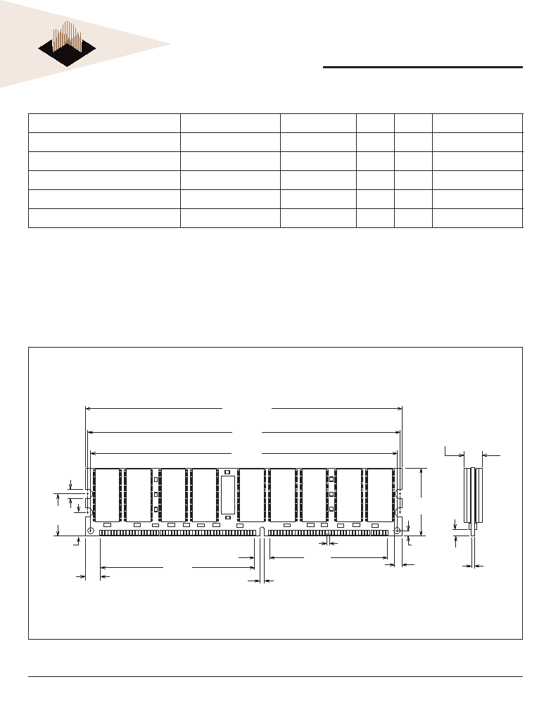
133.48
(5.255" MAX.)
3.99
(0.157 (2x))
17.78
(0.700)
10.0
(0.394)
6.36
(0.250)
64.77
(2.550)
1.78
(0.070)
49.53
(1.950)
3.00
(0.118)
(4x)
3.99
(0.157)
(MIN)
1.27
± 0.10
(0.050)
(± 0.004)
30.48
(1.20 MAX)
6.35
(0.250 MAX)
2.31
(0.091)
(2x)
1.27
(0.050 TYP.)
6.35
(0.250)
128.95
(5.077")
131.34
(5.171")
PACKAGE DIMENSIONS FOR JD3
* ALL DIMENSIONS ARE IN MILLIMETERS AND (INCHES).

W3EG72255S-D3
-JD3
-AJD3
12
White Electronic Designs
November 2004
Rev. 2
PRELIMINARY
White Electronic Designs Corporation ∑ (602) 437-1520 ∑ www.wedc.com
ORDERING INFORMATION FOR AJD3
Part Number
Speed
CAS Latency
t
RCD
t
RP
Height*
W3EG72255S335AJD3xG
166MHz/333Mb/s
2.5
3
3
28.70 (1.13")
W3EG72255S262AJD3xG
133MHz/266Mb/s
2
2
2
28.70 (1.13")
W3EG72255S263AJD3xG
133MHz/266Mb/s
2
3
3
28.70 (1.13")
W3EG72255S265AJD3xG
133MHz/266Mb/s
2.5
3
3
28.70 (1.13")
W3EG72255S202AJD3xG
100MHz/200Mb/s
2
2
2
28.70 (1.13")
NOTES:
∑ Consult Factory for availability of RoHS compliant products. (G = RoHS Compliant)
∑ Vendor specifi c part numbers are used to provide memory components source control. The place holder for this is shown as lower case "x" in the part numbers above and is to
be replaced with the respective vendors code. Consult factory for qualifi ed sourcing options. (M = Micron, S = Samsung & consult factory for others)
∑ Consult factory for availability of industrial temperature (-40∞C to 85∞C) option
133.48
(5.255" MAX.)
3.99
(0.157 (2x))
17.78
(0.700)
10.0
(0.394)
6.35
(0.250)
64.77
(2.550)
1.78
(0.070)
49.53
(1.950)
3.00
(0.118)
(4x)
3.99
(0.157)
(MIN)
1.27
± 0.10
(0.050)
(± 0.004)
28.70
(1.13 MAX)
6.35
(0.250 MAX)
2.31
(0.091)
(2x)
1.27
(0.050 TYP.)
6.35
(0.250)
128.95
(5.077")
131.34
(5.171")
PACKAGE DIMENSIONS FOR AJD3
* ALL DIMENSIONS ARE IN MILLIMETERS AND (INCHES).

W3EG72255S-D3
-JD3
-AJD3
13
White Electronic Designs
November 2004
Rev. 2
PRELIMINARY
White Electronic Designs Corporation ∑ (602) 437-1520 ∑ www.wedc.com
ORDERING INFORMATION FOR D3
Part Number
Speed
CAS Latency
t
RCD
t
RP
Height*
W3EG72255S335D3xG
166MHz/333Mb/s
2.5
3
3
28.58 (1.125")
W3EG72255S262D3xG
133MHz/266Mb/s
2
2
2
28.58 (1.125")
W3EG72255S263D3xG
133MHz/266Mb/s
2
3
3
28.58 (1.125")
W3EG72255S265D3xG
133MHz/266Mb/s
2.5
3
3
28.58 (1.125")
W3EG72255S202D3xG
100MHz/200Mb/s
2
2
2
28.58 (1.125")
NOTES:
∑ Consult Factory for availability of RoHS compliant products. (G = RoHS Compliant)
∑ Vendor specifi c part numbers are used to provide memory components source control. The place holder for this is shown as lower case "x" in the part numbers above and is to
be replaced with the respective vendors code. Consult factory for qualifi ed sourcing options. (M = Micron, S = Samsung & consult factory for others)
∑ Consult factory for availability of industrial temperature (-40∞C to 85∞C) option
133.48
(5.255" MAX.)
3.99
(0.157 (2x))
17.78
(0.700)
10.0
(0.394)
6.35
(0.250)
64.77
(2.550)
1.78
(0.070)
49.53
(1.950)
3.00
(0.118)
(4x)
3.99
(0.157)
(MIN)
1.27
± 0.10
(0.050)
(± 0.004)
28.58
(1.125 MAX)
6.35
(.250 MAX)
2.31
(0.091)
(2x)
1.27
(0.050 TYP.)
6.35
(0.250)
128.95
(5.077")
131.34
(5.171")
PACKAGE DIMENSIONS FOR D3
* ALL DIMENSIONS ARE IN MILLIMETERS AND (INCHES).
W3EG72255S-D3
-JD3
-AJD3
14
White Electronic Designs
November 2004
Rev. 2
PRELIMINARY
White Electronic Designs Corporation ∑ (602) 437-1520 ∑ www.wedc.com
PART NUMBERING GUIDE
W 3 E G 72 255M S xxx D3 x G
WEDC
SDRAM
DDR
GOLD
BUS WIDTH
DEPTH (Dual Rank):
256 = 256Mb
2.5V
SPEED (MHz):
166, 133, 100MHZ
PACKAGE:
JD3 or AJD3
COMPONENT VENDOR:
M = Micron, S = Samsung
RoHS COMPLIANT

W3EG72255S-D3
-JD3
-AJD3
15
White Electronic Designs
November 2004
Rev. 2
PRELIMINARY
White Electronic Designs Corporation ∑ (602) 437-1520 ∑ www.wedc.com
Document Title
2GB ≠ 2x128Mx72, DDR SDRAM Registered ECC, w/PLL
Revision History
Rev #
History
Release Date
Status
Rev 0
Initial Release
5-2-03
Advanced
Rev 1
Package dimension change
1.1 Added JD3 and AJD3 package options
1.2 Incorporated millimeter and inch measurements
1.3 Updated all abbreviations
1.4 Changed all / &
--
to #
1.5 Added "Not Recommended for New Designs" to D3
1.6 Added I
DD
specifi cations and test conditions for DDR
SDRAM components
1.7 Removed "ED" from part marking
1.8 Added document title page
3-3-04
Preliminary
Rev 2
2.1 Added Lead-Free and RoHS note
2.2 Added vendor code options
M = Micron
S = Samsung
11-04
Preliminary