
W90N740 Reference Manual
Publication Release Date: May 9, 2003
- 1 -
Revision A2
W90N740
32-Bit ARM7TDMI
-Based Micro-Controller
Reference Manual

W90N740 Reference Manual
- 2 -
The information described in this document is the exclusive intellectual property of
Winbond Electronics Corporation and shall not be reproduced without permission from Winbond.
Winbond is providing this document only for reference purposes of W90N740-based system design.
Winbond assumes no responsibility for errors or omissions.
All data and specifications are subject to change without notice.
For additional information or questions, please contact: Winbond Electronics Corp.

W90N740 Reference Manual
Publication Release Date: May 9, 2003
- 3 -
Revision A2
Table of Contents-
1.
GENERAL DESCRIPTION ............................................................................................................ 4
2.
FEATURES .................................................................................................................................... 4
3.
BLOCK DIAGRAM ......................................................................................................................... 8
4.
PIN CONFIGURATION .................................................................................................................. 9
4.1. Pin Assignment ..................................................................................................................... 10
5.
PIN DESCRIPTION...................................................................................................................... 13
6.
ELECTRICAL CHARACTERISTICS............................................................................................ 17
6.1. Absolute Maximum Ratings (To Be Added).......................................................................... 17
6.2. DC Characteristics ................................................................................................................ 18
6.2.1. Digital DC Characteristics (To Be Added) ...................................................................................18
6.2.2. USB Transceiver DC Characteristics (To Be Added) ..................................................................18
6.3. AC Characteristics ................................................................................................................ 19
6.3.1. EBI/SDRAM Interface AC Characteristics ...................................................................................19
6.3.2. EBI/External Master Interface AC Characteristics .......................................................................20
6.3.3. EBI/(ROM/SRAM/External I/O) AC Characteristics .....................................................................21
6.3.4. USB Transceiver AC Characteristics...........................................................................................22
6.3.5. EMC MII AC Characteristics........................................................................................................24
7.
PACKAGE DIAMENSION ............................................................................................................ 26
8.
W90N740 REGISTERS MAPPING TABLE ................................................................................. 27
9.
ORDERING INFORMATION........................................................................................................ 39
10.
REVISION HISTORY ................................................................................................................... 39

W90N740 Reference Manual
- 4 -
1. GENERAL DESCRIPTION
The W90N740 micro-controller is 16/32 bit, ARM7TDMI
based RISC micro-controller for network as
well as embedded applications. An integrated dual Ethernet MAC, the W90N740, is designed for use in
broadband routers, wireless access points, residential gateways and LAN camera.
The W90N740N is built around The ARM7TDMI
CPU core designed by Advanced RISC Machines, Ltd.
And achieves 80MHz under worse conditions. Its small size, fully static design is particularly suitable
for cost-sensitive and power-sensitive applications. It designs as Harvard architecture by offering an 8K-
byte I-cache/SRAM and an 2K-byte D-cache/SRAM with flexible configuration and two way set
associative structure to balance data movement between CPU and external memory. Four stages write
buffer also improves latency for write operations.
The external bus interface (EBI) controller provides single bus architecture, 8/16/32 bit data width to
access external SDRAM, ROM/SRAM, flash memory and I/O devices. It achieves same frequency as
CPU core to minimize latency if internal cache misses. Memory controller supports different kinds of
SDRAM types and configurations to ease system design. The System Manager includes an internal 32-
bit system bus arbiter and a PLL clock controller. Generic I/O bus is easily served as PCMCIA-like
interface for 802.11b wireless LAN connection.
Two 10/100Mb MACs of Ethernet controller is built in to reduce total system cost and increase
performance between WAN and LAN port. Either MII or RMII of MAC is selected for external 10/100
PHY chip to design for varieties of applications. A powerful NAT accelerator (Patent Pending) between
LAN and WAN reduces the software loading of CPU and speeds up performance between LAN and
WAN.
W90N740 integrates root hub of USB 1.1 host controller with one port transceiver and uses
additional port with external transceiver if necessary, which can add valuable functions like flash disk,
printer server, Bluetooth device via USB port. The important peripheral functions include one full wired
high speed UART channel, 2-Channel GDMA, one watch-dog timer, two 24-bit timers with 8-bit pre-
scale, 20 programmable I/O ports, and an advanced interrupt controller.
2. FEATURES
Architecture
� Highly-integrated system for embedded Ethernet applications
� Powerful ARM7TDMI
core and fully 16/32-bit RISC architecture
� Big /Little-Endian mode supported
� Cost-effective JTAG-based debug solution
System Manager
� System memory map & on-chip peripherals memory map
� The data bus width of external memory address & data bus connection with external memory
� Bus arbitration supports the Fixed Priority Mode & Rotate Priority Mode
� Power-On setting
� On-Chip PLL module control & Clock select control

W90N740 Reference Manual
Publication Release Date: May 9, 2003
- 5 -
Revision A2
External Bus Interface (EBI)
� External I/O Control with 8/16/32 bit external data bus
� Cost-effective memory-to-peripheral DMA interface
� SDRAM Controller supports up to 2 external SDRAM & the maximum size of each device is 32MB
� ROM/FLASH & External I/O interface
� Support for PCMCIA 16-bit PC Card devices
On-Chip Instruction and Data Cache
� Two-way, Set-associative, 8K-byte I-cache and 2K-byte D-cache
� Support for LRU (Least Recently Used) Protocol
� Cache can be configured as an internal SRAM
� Support Cache Lock function
Ethernet MAC Controller (EMC)
� IEEE 802.3 protocol engine with programmable MII or RMII interface for 10/100 Mbits/s
� DMA engine with burst mode
� 256 bytes transmit & 256 bytes receive FIFO for MAC protocol engine and DMA access
� Built-in 16 entry CAM Address Register
� Support long frame (more than 1518 bytes) and short frame (less than 64 bytes)
� Re-transmit (during collision) the frame without DMA access
� Half or full duplex function option
� Support Station Management for external PHY
� On-Chip Pad generation
NAT Accelerator (Patent Pending)
� Hardware acceleration on IP address / port number look up and replacement for network address
translation, including MAC address translation
� Provide 64 entries of translation table
� Support TCP / UDP packets
GDMA Controller
� 2 Channel GDMA for memory-to-memory data transfers without CPU intervention
� Increase or decrease source / destination address in 8-bit, 16-bit, or 32-bit data transfers
� Supports 4-data burst mode to boost performance
� Support external GDMA request

W90N740 Reference Manual
- 6 -
USB Host Controller
� USB 1.1 compatible
� Open Host Controller Interface (OHCI) 1.0 compatible.
� Supports both low-speed (1.5 Mbps) and full-speed (12Mbps) USB devices.
� Built-in DMA for real-time data transfer
UART
� One UART (serial I/O) blocks with interrupt-based operation
� Full set of MODEM control functions (CTS, RTS, DSR, DTR, RI and DCD)
� Fully programmable serial-interface characteristics:
� Break generation and detection
� False start bit detection
� Parity, overrun, and framing error detection
� Full prioritized interrupt system controls
Timers
� Two programmable 24-bit timers with 8-bit pre-scalar
� One programmable 24-bit Watch-Dog timer
� One-short mode, period mode or toggle mode operation
Programmable I/Os
� 21 programmable I/O ports
I
� /O ports Configurable for Multiple functions
Advanced Interrupt Controller (AIC)
� 18 interrupt sources, including 4 external interrupt sources
� Programmable normal or fast interrupt mode (IRQ, FIQ)
� Programmable as either edge-triggered or level-sensitive for 4 external interrupt sources
� Programmable as either low-active or high-active for 4 external interrupt sources
� Priority methodology is encoded to allow for interrupt daisy-chaining
� Automatically mask out the lower priority interrupt during interrupt nesting
GPIO Controller
� Programmable as an input or output pin

W90N740 Reference Manual
Publication Release Date: May 9, 2003
- 7 -
Revision A2
On-Chip PLL
� One PLL for both CPU and USB host controller
� The external clock can be multiplied by on-chip PLL to provide high frequency system clock
� Programmable clock frequency, and the input frequency range is 3-30MHz; 15MHz is preferred.
Operation Voltage Range
� 2.7 � 3.6 V for IO Buffer
� 1.62 � 1.98 V for Core Logic
Operation Temperature Range
� 0 � 70 Degree C
Operating Frequency
� 80 MHz (default)
Package Type
� 176-pin LQFP

W90N740 Reference Manual
- 8 -
3. BLOCK DIAGRAM
ARM7TDMI
Cache
Controller
Wrapper
APB
Bridge
AHB
Arbiter
AHB
Decoder
UART
TIMER x2
Interrupt
Controller
GPIO
Clock
Controller
PLL
External Bus
Controller
GDMA
Controller
USB Host
Controller
Ethenet
MAC
Controller 0
W90N740
8K-Byte
I Cache
ROM
Flash
RAM
PCMCIA
IO Dev
SDRAM
USB
Device
PHY
PHY
AHB
B
u
s
A
P
B Bus
TDMI Bus
2K-Byte
D Cache
JTAG
ICE
EBI Bus
COM Port
External
Interrupts
WDT
NAT
Accelerator
Ethenet
MAC
Controller 1
Fig 3.1 W90N740 Functional Block Diagram

W90N740 Reference Manual
Publication Release Date: May 9, 2003
- 9 -
Revision A2
4. PIN CONFIGURATION
85
140
50
55
60
80
75
70
65
165
160
155
150
145
175
170
VDD18
VSS18
VDD33
VDD33
VSS33
G
P
18/
nIRQ1
G
P
17/
nIRQ0
G
P
20/
nIRQ3
G
P
19/
nIRQ2
GP12/nWDOG
GP14/TIMER1
GP13/TIMER0
EXTAL
XT
AL
TMS
TCK
nRESET
nTRST
TDO
TDI
USBVSS
USBVDD
DN
DP
D29
D28
D31
D30
SD
QM
3
VSS33
D13
D12
D15
D14
SDQM1
NC
NC
MDIO1
A1
2
A1
1
A1
0
A9
A8
A7
A6
A5
A4
A3
MCKE
nS
W
E
VD
D
1
8
VSS1
8
VDD
3
3
VD
D
3
3
V
SS3
3
VSS3
3
MCL
K
A0
A2
A1
D7
D6
D5
D4
D27
D26
D25
D24
nS
C
A
S
nS
R
A
S
D23
D22
D21
D20
D11
D10
D9
D8
EMREQ
nOE
nECS0
nBTCS
nWAIT
EMACK
nECS3
nECS2
nECS1
VDD18
VSS18
VDD33
VDD33
VSS33
VSS33
GP15/nXDACK
GP16/nXDREQ
A1
9
A1
8
A1
7
A1
6
A1
5
A1
4
A1
3
nSCS1
nSCS0
D3
D2
D1
D0
SDQM0
D19
D18
D17
D16
SD
QM
2
GP0
GP3
GP2
GP1
M
DC0
A2
4
A2
3
A2
2
A2
1
A2
0
TX0_
CLK
CRS
0
CO
L0
MD
IO
0
RX
0_
E
R
R
R
X
0_C
LK
TX
0
D
0
TX0_E
N
TX
0
D
3
TX
0
D
2
TX
0
D
1
RX
0
D
0
RX
0
D
3
RX
0
D
2
RX
0
D
1
RX0_D
V
VD
D
1
8
V
SS1
8
VD
D
3
3
VD
D
3
3
AVD
D
1
8
V
SS3
3
V
SS3
3
A
VSS1
8
D
VSS1
8
DV
DD
1
8
G
P
11/
R
x
D
G
P
10/
Tx
D
GP9/nDSR
GP4/nRI
GP
5
/
n
R
TS
GP
6
/
n
C
TS
GP7/nCD
GP8/nDTR
135
MDC1
COL1
CRS1
TX1CLK
TX1D3
TX1D2
TX1D0
TX1D1
RX
1
D
0
5
10
15
20
25
30
35
40
95
90
120
110
105
100
130
125
RX
1
D
3
RX
1
D
2
RX
1
D
1
TX1EN
RX
1
_
E
RR
RX
1_
DV
R
X
1_C
LK
W90N740
176-Pin LQFP
VSS3
3
VDD
3
3
115
Fig 4.1 176-Pin LQFP Pin Diagram

W90N740 Reference Manual
- 10 -
4.1. Pin Assignment
PIN NAME
176-PIN LQFP
Clock & Reset
( 4 pins )
EXTAL
164
XTAL
163
MCLK
54
nRESET
27
TAP Interface
( 5 pins )
TCK
25
TMS
20
TDI
21
TDO
24
nTRST
26
External Bus Interface
( 78 pins )
A [24:22]
84-82
A [21:0]
81-74,72,70,
67-56
D [31:16]
124-119,117,
115-114,111-105
D [15:0]
104-103,101,
99-88,86
nWBE [3:0]/ SDQM [3:0]
46-43
nSCS[1:0]
42,41
NSRAS
51
NSCAS
52
NSWE
50
MCKE
49
NC
48
NC
47
EMREQ
31
EMACK
30
nWAIT
32
NBTCS
40
nECS[3:0]
39-36
NOE
34
W90N740 Reference Manual
Publication Release Date: May 9, 2003
- 11 -
Revision A2
Pins Assignment, Continued
PIN NAME
176-PIN LQFP
Ethernet Interface (0)
( 17 pins )
MDC0
142
MDIO0
143
COL0 /
151
CRS0 /
R1B_CRSDV
152
TX0_CLK
150
TX0D [3:0] / R1B_TXD [1:0],
R0_TXD [1:0]
149-146
TX0_EN / R0_TXEN
144
RX0_CLK / R0_REFCLK
153
RX0D [3:0] / R1B_RXD [1:0],
R0_RXD [1:0]
159-157,154
RX0_DV / R0_CRSDV
160
RX0_ERR
161
Ethernet Interface (1)
( 17 pins )
MDC1
10
MDIO1
8
COL1
6
CRS1
7
TX1_CLK
11
TX1D [3:0] / R1A_TX [1:0]
4-1
TX1_EN /R1A_TXEN
5
RX1_CLK / R1A_REFCLK
167
RX1D [3:0] / R1A_RXD [1:0]
172-169
RX1_DV / R1A_CRSDV
168
RX1_ERR / R1A_RXERR
166

W90N740 Reference Manual
- 12 -
Pins Assignment, Continued
NAME
176-PIN LQFP
USB Interface
( 2 pins )
DP
131
DN
130
Miscellaneous
( 21 pins )
GP [20:17] / nIRQ [3:0]
136-133
GP16 / nXDREQ
29
GP15 /nXDACK
28
GP14 /
TIMER1/ SPEED
19
GP13 /
TIMER0/ STDBY
18
GP12 /nWDOG
17
GP11 /RxD
140
GP10 /TxD
139
GP9/nDSR/nTOE
128
GP8 /nDTR/FSE0
127
GP7 /nCD / VO
126
GP6 /nCTS/ VM
138
GP5 /nRTS/ VP
137
GP4 /nRI / RCV
125
GP [3:0]
16-13
Name
176-Pin LQFP
Power/Ground
(32 pins)
VDD18
22,69,113,155
VSS18
23,68,112,156
VDD33
12,33,53,71,85,
100,116,141,162
VSS33
9,35,55,73,87,102,118,145
,165
USBVDD
132
USBVSS
129
DVDD18
175
DVSS18
176
AVDD18
173
AVSS18
174

W90N740 Reference Manual
Publication Release Date: May 9, 2003
- 13 -
Revision A2
5. PIN DESCRIPTION
PIN NAME
IO TYPE
DESCRIPTION
System Clock & Reset
EXTAL
I
External Clock / Crystal Input
XTAL O
Crystal
Output
MCLK
O
System Master Clock Out, SDRAM clock
nRESET I
System
Reset,
active-low
TAP Interface
TCK ID
JTAG
Clock,
internal pull-down with 58K ohm
TMS
IU
JTAG Mode Select, internal pull-up with 70K ohm
TDI
IU
JTAG Data in, internal pull-up with 70K ohm
TDO
O
JTAG Data out
nTRST
IU
JTAG Reset, active-low, internal pull-up with 70K ohm
External Bus Interface
A [24:22]
O
Address Bus (MSB) of external memory and IO devices
A [21:0]
IO
Address Bus of external memory and IO devices
D [31:16]
IO
Data Bus (MSB) of external memory and IO device, internal pull-up with 70K ohm.
D [15:0]
IO
Data Bus (LSB) of external memory and IO device
nWBE [3:0]/
SDQM [3:0]
IO
Write Byte Enable for specific device(nECS[3:0]),
Data input/output Mask signal for SDRAM (nSCS[1:0]), active-low
nSCS [1:0]
O
SDRAM chip select for two external banks, active-low.
nSRAS
O
Row Address Strobe for SDRAM, active-low
nSCAS
O
Column Address Strobe for SDRAM, active-low
nSWE
O
SDRAM Write Enable, active-low
MCKE
O
SDRAM Clock Enable, active-high
NC ID
NC O
EMREQ ID
External Master Bus Request
This is used to request external bus. When EMACK active, indicates the bus grants
the bus, chip drives all the output pins of the external bus to high impedance.
EMACK
O
External Bus Acknowledge
nWAIT
IU
External Wait, active-low
This pin indicates that the external devices need more active cycle during access
operation.
nBTCS
O
ROM/Flash Chip Select, active-low
nECS [3:0]
IO
External I/O Chip Select, active-low.
nOE
O
ROM/Flash, External Memory Output Enable, active-low

W90N740 Reference Manual
- 14 -
Pins Description, Continued
PIN NAME
IO TYPE
DESCRIPTION
Ethernet Interface (0)
MDC0 O
MII Management Data Clock for Ethernet 0. It is the reference clock of MDIO0. Each
MDIO0 data will be latched at the rising edge of MDC0 clock.
MDIO0 IO
MII Management Data I/O for Ethernet 0. It is used to transfer MII control and status
information between PHY and MAC.
COL0
I
Collision Detect for Ethernet 0 in MII mode. This shall be asserted by PHY upon
detecting a collision happened over the medium. It will be asserted and lasted until
collision condition vanishes.
CRS0
I
Carrier Sense for Ethernet 0 in MII mode.
TX0_CLK I
Transmit Data Clock for Ethernet 0 in MII mode.
TX0_CLK is driven by PHY and
provides the timing reference for TX0_EN and TX0D. The clock will be 25MHz or 2.5
MHz.
TX0D [3:0] /
R0_TXD [1:0]
O
Transmit Data bus (4-bit) for Ethernet 0 in MII mode. The nibble transmit data bus is
synchronized with TX0_CLK. It should be latched by PHY at the rising edge of TX0_CLK.
In RMII mode, TX0D [1:0] are used as R0_TXD [1:0],2-bit Transmit Data bus for Ethernet
0.
TX0_EN /
R0_TXEN
O
Transmit Enable for Ethernet 0 in MII. It indicates the transmit activity to external PHY.
It will be synchronized with TX0_CLK.
In RMII mode, R0_TXEN shall be asserted synchronously with the first nibble of the
preamble and shall remain asserted while all di-bits to be transmitted are presented. Of
course, it is synchronized with R0_REFCLK.
RX0_CLK /
R0_REFCLK
I
Receive Data Clock for Ethernet 0 in MII mode When it is used as a received clock
pin, it is from PHY. The clock will be either 25 MHz or 2.5 MHz. The minimum duty cycle
at its high or low state should be 35% of the nominal period for all conditions.
In RMII mode, this pin is used as R0_REFCLK, Reference Clock;
The clock shall be
50MHz +/- 50 ppm with minimum 35% duty cycle at high or low state.
RX0D [3:0] /
R0_RXD [1:0]
I
Receive Data bus (4-bit) for Ethernet 0 in MII mode. They are driven by external PHY,
and should be synchronized with RX0_CLK and valid only when RX0_DV is valid.
In RMII mode, RX0D [1:0] are used as R0_RXD [1:0], 2-bit Receive Data bus for
Ethernet 0.
RX0_DV /
R0_CRSDV
I
Receive Data Valid for Ethernet 0 in MII mode. It will be asserted when received data is
coming and present, and de-asserted at the end of the frame.
In RMII mode, this pin is used as the R0_CRSDV, Carrier Sense / Receive Data Valid for
Ethernet 0. The R0_CRSDV shall be asserted by PHY when the receive medium is non-
idle. Loss of carrier shall result in the de-assertion of R0_CRSDV synchronous to the
cycle of R0_REFCLK, and only on nibble boundaries.
RX0_ERR
I
Receive Data Error for Ethernet 0 in MII mode. It indicates a data error detected by
PHY. The assertion should be lasted for longer than a period of RX0_CLK. When
RX0_ERR is asserted, the MAC will report a CRC error.

W90N740 Reference Manual
Publication Release Date: May 9, 2003
- 15 -
Revision A2
Pins Description, Continued
PIN NAME
IO TYPE
DESCRIPTION
Ethernet Interface (1)
MDC1 O
MII Management Data Clock for Ethernet 1. It is the reference clock of MDIO1. Each
MDIO1 data will be latched at the rising edge of MDC1 clock.
MDIO1 IOU
MII Management Data I/O for Ethernet 1. It is used to transfer MII control and status
information between PHY and MAC.
COL1 IU
Collision Detect for Ethernet 1 in MII mode. This shall be asserted by PHY upon
detecting a collision happened over the medium. It will be asserted and lasted until
collision condition vanishes.
CRS1
IU
Carrier Sense for Ethernet 1 in MII mode.
TX1_CLK IU
Transmit Data Clock for Ethernet 1 in MII mode, TX1_CLK is driven by PHY and
provides the timing reference for TX1_EN and TX1D. The clock will be 25MHz or 2.5
MHz.
TX1D [3:0] /
R1A_TXD [1:0]
O
Transmit Data bus (4-bit) for Ethernet 1 in MII mode. The nibble transmit data bus is
synchronized with TX1_CLK. It should be latched by PHY at the rising edge of
TX1_CLK.
In RMII mode, TX1D [1:0] are used as R1A_TXD [1:0], 2-bit Transmit Data bus for
Ethernet 1.
TX1_EN/
R1A_TXEN
O
Transmit Enable for Ethernet 1 in MII and RMII mode. It indicates the transmit
activity to external PHY. It will be synchronized with TX1_CLK in MII mode.
RX1_CLK /
R1A_REFCLK
IU
Receive Data Clock for Ethernet 1 in MII mode. When it is used as a received clock
pin, it is from PHY. The clock will be either 25 MHz or 2.5 MHz. The minimum duty
cycle at its high or low state should be 35% of the nominal period for all conditions.
In RMII mode, this pin is used as R1A_REFCLK. The clock shall be 50MHz +/-50 ppm
with minimum 35% duty cycle at high or low state.
RX1D [3:0] /
R1A_RXD[1:0]
IU
Receive Data bus (4-bit) for Ethernet 1 in MII mode. They are driven by external
PHY, and should be synchronized with RX1_CLK and valid only when RX1_DV is
valid.
In RMII mode, RX1D [1:0] are used as R1A_RXD [1:0], 2-bit Receive Data bus for
Ethernet 1.
RX1_DV/
R1A_CRSDV
IU
Receive Data Valid for Ethernet 1 in MII mode. It will be asserted when received data is
coming and present, and de-asserted at the end of the frame.
In RMII mode, this pin is used as the R1A_CRSDV, Carrier Sense / Receive Data Valid
for Ethernet 1. The R1A_CRSDV shall be asserted by PHY when the receive medium
is non-idle. Loss of carrier shall result in the de-assertion of R1A_CRSDV synchronous
to the cycle of R1A_REFCLK, and only on nibble boundaries.
RX1_ERR /
R1A_RXERR
IU
Receive Data Error for Ethernet 1 in MII and RMII mode. It indicates a data error
detected by PHY. The assertion should be lasted for longer than a period of RX0_CLK.
When RX0_ERR is asserted, the MAC will report a CRC error.

W90N740 Reference Manual
- 16 -
Pins Description, Continued
NAME
IO TYPE
DESCRIPTION
USB Interface
DP
IO
Differential Positive USB IO signal
DN
IO
Differential Negative (Minus) USB IO signal
Miscellaneous
GP[20:17] / nIRQ[3:0]
IO
External Interrupt Request or General Purpose I/O
GP16 / nXDREQ
IO
External DMA Request or General Purpose I/O
GP15 /nXDACK
IO
External DMA Acknowledge or General Purpose I/O
GP14 /
TIMER1/SPEED
IO
Timer 1 or General Purpose I/O. This pin is also used as SPEED,
Speed mode control for external USB transceiver
GP13 /
TIMER0/STDBY
IO
Timer 0 or General Purpose I/O. This pin is also used as STDBY, StandBy
control for external USB transceiver
GP12 /nWDOG
IO
Watchdog Timer Timeout Flag (active-low) or General Purpose I/O
GP11 /RxD
IO
UART Receive Data or General Purpose I/O
GP10 /TxD
IO
UART Transmit Data or General Purpose I/O
GP9/nDSR/nTOE IOU
UART Receive Clock or General Purpose I/O. This pin is also used as nTOE,
Output Enable control (active-low) for external USB transceiver.
GP8 /nDTR/FSE0
IOU
UART Transmit Clock or General Purpose I/O. This pin is also used as SE0,
Differential Data Transceiver Output for external USB transceiver.
GP7 /nCD /VO
IOU
UART Carrier Detector or General Purpose I/O. This pin is also used as VO,
Data Output for external USB transceiver.
GP6 /nCTS/ VM
IOU
UART Clear to Send or General Purpose I/O. This pin is also used as VM, Data
Negative (Minus) Input for external USB receiver.
GP5 /nRTS/ VP
IOU
UART Ready to Send or General Purpose I/O. This pin is also used as VP, Data
Positive Input for external USB receiver.
GP4 /nRI /RCV
IOU
UART Ring Indicator or General Purpose I/O. This pin is also used as RCV,
Difference Receiver Input.
GP[3:0]
IOU
General Purpose I/O.
Power/Ground
VDD18
P
Core Logic power (1.8V)
VSS18
G
Core Logic ground (0V)
VDD33
P
IO Buffer power (3.3V)
VSS33
G
IO Buffer ground (0V)
USBVDD
P
USB power (3.3V)
USBVSS
G
USB ground (0V)
DVDD18
P
PLL Digital power (1.8V)
DVSS18
G
PLL Digital ground (0V)
AVDD18
P
PLL Analog power (1.8V)
AVSS18
G
PLL Analog ground (0V)

W90N740 Reference Manual
Publication Release Date: May 9, 2003
- 17 -
Revision A2
6. ELECTRICAL CHARACTERISTICS
6.1. Absolute Maximum Ratings (To Be Added)
Ambient Temperature .............................................................................
Storage Temperature ............................................................................
Voltage on Any Pin ...............................................................................
Power Supply Voltage (Core logic) ............................................................
Power Supply Voltage (IO Buffer) .............................................................
Injection Current (latch-up testing) .........................................................
Crystal Frequency ....................................................................................
W90N740 Reference Manual
- 18 -
6.2. DC Characteristics
6.2.1. Digital DC Characteristics (To Be Added)
SYMBOL PARAMETER CONDITION
MIN.
MAX.
UNIT
V
DD
33/
USBVDD
Power Supply
V
V
DD
18/
DVDD18/
AVDD18
Power Supply
V
V
IL
Input Low Voltage
V
V
IH
Input High Voltage
V
VT+
Schmitt Trigger positive-going threshold
V
VT-
Schmitt trigger negative-going threshold
V
V
OL
Output Low Voltage
V
V
OH
Output High Voltage
V
I
CC
Supply Current
mA
I
IH
Input High Current
�A
I
IL
Input Low Current
�A
I
IHP
Input High Current (pull-up)
�A
I
ILP
Input Low Current (pull-up)
�A
I
IHD
Input High Current (pull-down)
�A
I
ILD
Input Low Current (pull-down)
�A
6.2.2. USB Transceiver DC Characteristics (To Be Added)
SYMBOL PARAMETER CONDITIONS
MIN.
MAX.
UNIT
V
DI
Differential Input Sensitivity
V
V
CM
Differential Common Mode Range
V
V
SE
Single Ended Receiver Threshold
V
V
OL
Static Output Low Voltage
V
V
OH
Static Output High Voltage
V
V
CRS
Output Signal Crossover Voltage
V
Z
DRV
Driver Output Resistance
C
IN
Pin
Capacitance
pF
W90N740 Reference Manual
Publication Release Date: May 9, 2003
- 19 -
Revision A2
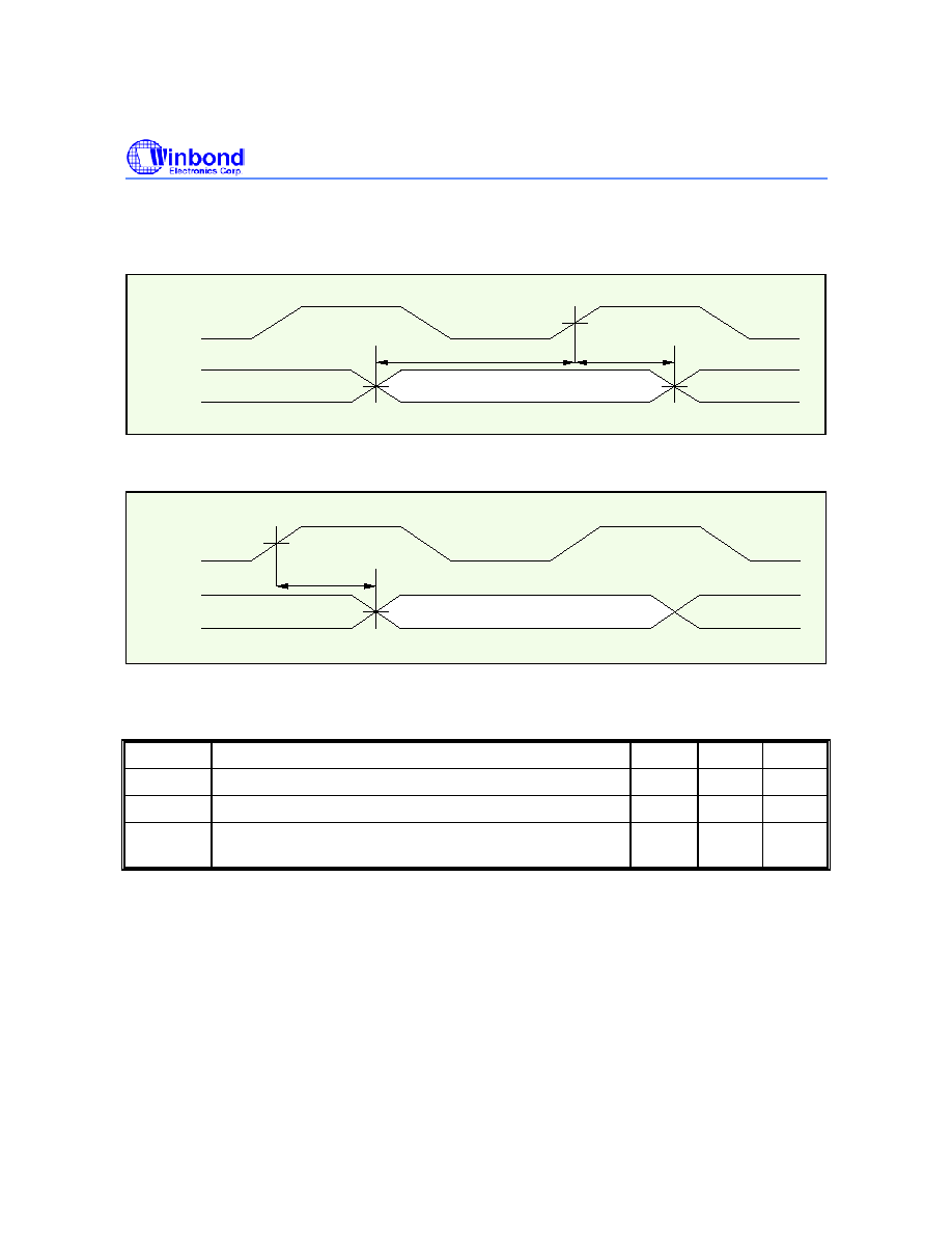
6.3. AC Characteristics
6.3.1. EBI/SDRAM Interface AC Characteristics
MCLK
D[31:0]
Input Valid
1.5V
1.5V
1.5V
T
DSU
T
DH
MCLK
Output
Delay
Output Valid
1.5V
1.5V
T
DO
SYMBOL PARAMETER MIN.
MAX.
UNIT
T
DSU
D [31:0] Setup Time
nS
T
DH
D [31:0] Hold Time
nS
T
DO
D [31:0], A [24:0], nSCS [1:0], SDQM [3:0], CKE, nSWE,
nSRAS, nSCAS
nS
W90N740 Reference Manual
- 20 -
6.3.2. EBI/External Master Interface AC Characteristics
MCLK
T
EMSU
EMREQ
EMACK
T
EMAO
T
EMH
T
EMAO
SYMBOL DESCRIPTION MIN
MAX
UNIT
T
EMSU
EMREQ Setup Time
nS
T
EMH
EMREQ Hold Time
nS
T
EMAO
EMACK Output Delay Time
nS
W90N740 Reference Manual
Publication Release Date: May 9, 2003
- 21 -
Revision A2
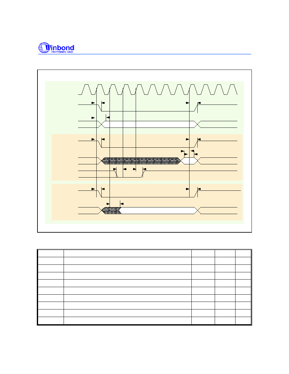
6.3.3. EBI/(ROM/SRAM/External I/O) AC Characteristics
Address Valid
R Data
Write Data Vaild
MCLK
T
DO
nECS[3:0]
A[24:0]
nOE
D[31:0]
nWAIT
nWBE[3:0]
D[31:0]
T
NECSO
T
NECSO
T
ADDO
T
NOEO
T
NOEO
T
DSU
T
DH
T
NWAH
T
NWBO
T
NWBO
T
NWASU
(To Be Added)
SYMBOL DESCRIPTION MIN.
MAX.
UNIT
T
ADDO
Address Output Delay Time
nS
T
NCSO
ROM/SRAM/Flash or External I/O Chip Select Delay Time
nS
T
NOEO
ROM/SRAM or External I/O Bank Output Enable Delay
nS
T
NWBO
ROM/SRAM or External I/O Bank Write Byte Enable Delay
nS
T
DH
Read Data Hold Time
nS
T
DSU
Read Data Setup Time
nS
T
DO
Write Data Output Delay Time (SRAM or External I/O)
nS
T
NWASU
External Wait Setup Time
nS
T
NWAH
External Wait Hold Time
nS
W90N740 Reference Manual
- 22 -
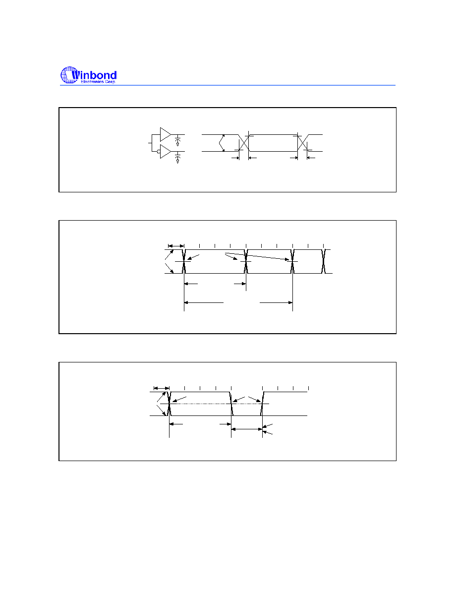
6.3.4. USB Transceiver AC Characteristics
Low Speed: 75ns at C
L
= 50pF, 300ns at C
L
= 350pF
Full Speed: 4 to 20ns at C
L
= 50pF
Differential
Data Lines
10%
Rise Time
90%
Fall Time
t
F
t
R
10%
90%
C
L
C
L
Data Signal Rise and Fall Time
T
PERIOD
Differential
Data Lines
Crossover
Points
Paired
Transitions
N * T
PERIOD
+ T
xJR2
Consecutive
Transitions
N * T
PERIOD
+ T
xJR1
Differential Data Jitter
T
PERIOD
Differential
Data Lines
Crossover
Point
Crossover
Point Extended
Source EOP Width: T
EOPT
Receiver EOP Width: T
EOPR1
, T
EOPR2
Diff. Data to
SE0 Skew
N * T
PERIOD
+ T
DEOP
Differential to EOP Transition Skew and EOP Width
W90N740 Reference Manual
Publication Release Date: May 9, 2003
- 23 -
Revision A2
Differential
Data Lines
Paired
Transitions
N * T
PERIOD
+ T
JR2
T
PERIOD
Consecutive
Transitions
N * T
PERIOD
+ T
JR1
T
JR
T
JR1
T
JR2
Receiver Jitter Tolerance
USB Transceiver AC Characteristics (To Be Added)
SYMBOL DESCRIPTION CONDITIONS
MIN.
MAX.
UNIT
T
R
Rise Time
nS
T
F
Fall Time
nS
T
RFM
Rise/Fall Time Matching
%
T
DRATE
Full Speed Data Rate
Mbps
T
DJ1
T
DJ2
Source Differential Driver Jitter
To Next Transition
For Paired Transitions
nS
T
EOPT
Source EOP Width
nS
T
DEOP
Differential to EOP Transition Skew
nS
T
JR1
T
JR2
Receiver Data Jitter Tolerance
To Next Transition
For Paired Transitions
nS
T
EOPR1
T
EOPR2
EOP Width at Receiver
Must Reject as EOP
Must Accept as EOP
nS

W90N740 Reference Manual
- 24 -
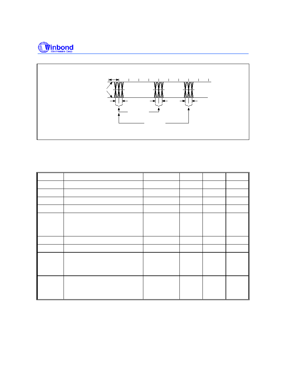
6.3.5. EMC MII AC Characteristics
The signal timing characteristics conforms to the guidelines specified in IEEE Std. 802.3.
TX_CLK
TX_D [3:0]
TX_EN
TX_ERR
T
TXO
Valid
Transmit Signal Timing Relationships at MII
RX_CLK
RX_D [3:0]
RX_DV
RX_ERR
VALID
INPUT
T
RXH
T
RXSU
Receive Signal Timing Relationships at MII
(To Be Added)
SYMBOL DESCRIPTION MIN.
MAX.
UNIT
T
TXO
Transmit Output Delay Time
nS
T
RXSU
Receive Setup Time
nS
T
RXH
Receive Hold Time
nS

W90N740 Reference Manual
Publication Release Date: May 9, 2003
- 25 -
Revision A2
Continued
MDC
MDIO
VALID
INPUT
T
MDH
T
MDSU
MDIO Read From PHY Timing
MDC
MDIO
T
MDO
Valid
MDIO Write to PHY Timing
(To Be Added)
SYMBOL DESCRIPTION MIN.
MAX.
UNIT
T
MDO
MDIO Output Delay Time
nS
T
MDSU
MDIO Setup Time
nS
T
MDH
MDIO Hold Time
nS
W90N740 Reference Manual
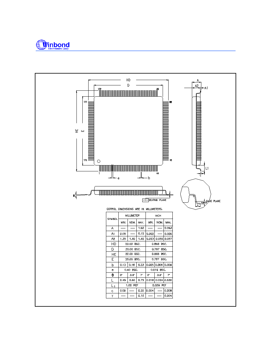
- 26 -
7. PACKAGE DIAMENSION
176-Pin LQFP
W90N740 Reference Manual
Publication Release Date: May 9, 2003
- 27 -
Revision A2
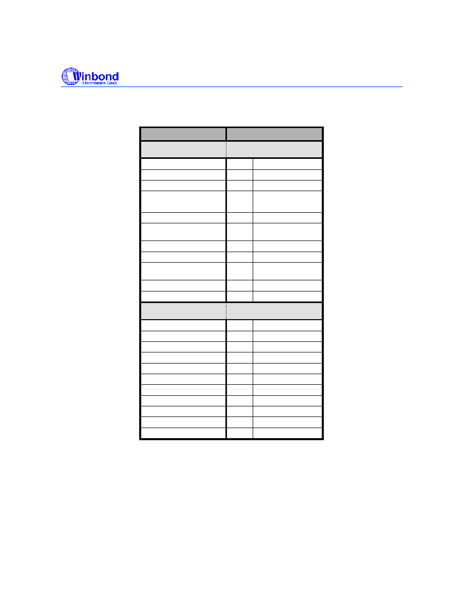
8. W90N740 REGISTERS MAPPING TABLE
R: read only, W: write only, R/W: both read and write, C: Only value 0 can be written
System Manager Control Registers Map
REGISTER ADDRESS R/W
DESCRIPTION
RESET
VALUE
PDID 0xFFF0.0000
R
Product
Identifier Register
0xX090.0740
ARBCON 0xFFF0.0004
R/W
Arbitration Control Register
0x0000.0000
PLLCON 0xFFF0.0008
R/W
PLL
Control Register
0x0000.2F01
CLKSEL 0xFFF0.000C
R/W
Clock
Select Register
0x0000.3FX8
EBI Control Registers Map
REGISTER ADDRESS R/W
DESCRIPTION
RESET
VALUE
EBICON 0xFFF0.1000
R/W
EBI
control register
0x0001.0000
ROMCON 0xFFF0.1004 R/W ROM/FLASH
control register
0x0000.0XFC
SDCONF0 0xFFF0.1008 R/W SDRAM bank 0 configuration register
0x0000.0800
SDCONF1 0xFFF0.100C R/W SDRAM
bank
1 configuration register
0x0000.0800
SDTIME0
0xFFF0.1010 R/W SDRAM bank 0 timing control register
0x0000.0000
SDTIME1
0xFFF0.1014 R/W SDRAM bank 1 timing control register
0x0000.0000
EXT0CON 0xFFF0.1018 R/W External
I/O 0 control register
0x0000.0000
EXT1CON 0xFFF0.101C R/W External
I/O 1 control register
0x0000.0000
EXT2CON 0xFFF0.1020 R/W External
I/O 2 control register
0x0000.0000
EXT3CON 0xFFF0.1024 R/W External
I/O 3 control register
0x0000.0000
CKSKEW
0xFFF0.1F00 R/W Clock skew control register
0xXXXX.0038
Cache Control Registers Map
REGISTER ADDRESS R/W
DESCRIPTION
RESET
VALUE
CAHCNF 0xFFF0.2000
R/W
Cache
configuration register
0x0000.0000
CAHCON 0xFFF0.2004
R/W
Cache
control register
0x0000.0000
CAHADR 0xFFF0.2008
R/W
Cache
address register
0x0000.0000

W90N740 Reference Manual
- 28 -
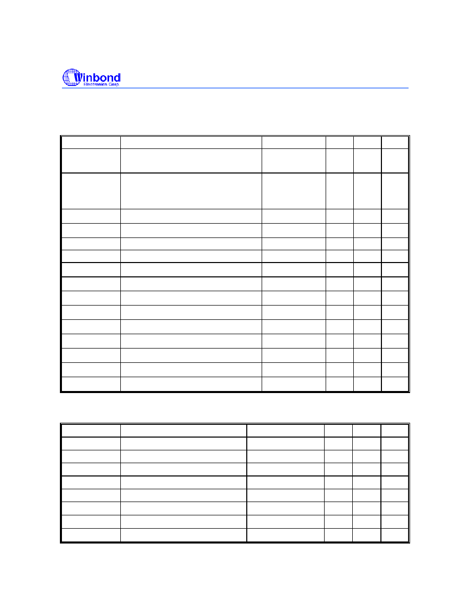
EMC 0 Control registers Map
REGISTER ADDRESS R/W
DESCRIPTION
RESET
VALUE
CAM REGISTERS
CAMCMR_0 0xFFF0.3000 R/W CAM
Command Register
0x0000.0000
CAMEN_0 0xFFF0.3004
R/W
CAM enable register
0x0000.0000
CAM1M_0
0xFFF0.3008
R/W
CAM1 Most Significant Word Register
0x0000.0000
CAM1L_0
0xFFF0.300C
R/W
CAM1 Least Significant Word Register
0x0000.0000
CAM2M_0
0xFFF0.3010
R/W
CAM2 Most Significant Word Register
0x0000.0000
CAM2L_0
0xFFF0.3014
R/W
CAM2 Least Significant Word Register
0x0000.0000
CAM3M_0
0xFFF0.3018
R/W
CAM3 Most Significant Word Register
0x0000.0000
CAM3L_0
0xFFF0.301C
R/W
CAM3 Least Significant Word Register
0x0000.0000
CAM4M_0
0xFFF0.3020
R/W
CAM4 Most Significant Word Register
0x0000.0000
CAM4L_0
0xFFF0.3024
R/W
CAM4 Least Significant Word Register
0x0000.0000
CAM5M_0
0xFFF0.3028
R/W
CAM5 Most Significant Word Register
0x0000.0000
CAM5L_0
0xFFF0.302C
R/W
CAM5 Least Significant Word Register
0x0000.0000
CAM6M_0
0xFFF0.3030
R/W
CAM6 Most Significant Word Register
0x0000.0000
CAM6L_0
0xFFF0.3034
R/W
CAM6 Least Significant Word Register
0x0000.0000
CAM7M_0
0xFFF0.3038
R/W
CAM7 Most Significant Word Register
0x0000.0000
CAM7L_0
0xFFF0.303C
R/W
CAM7 Least Significant Word Register
0x0000.0000
CAM8M_0
0xFFF0.3040
R/W
CAM8 Most Significant Word Register
0x0000.0000
CAM8L_0
0xFFF0.3044
R/W
CAM8 Least Significant Word Register
0x0000.0000
CAM9M_0
0xFFF0.3048
R/W
CAM9 Most Significant Word Register
0x0000.0000
CAM9L_0
0xFFF0.304C
R/W
CAM9 Least Significant Word Register
0x0000.0000
CAM10M_0
0xFFF0.3050
R/W
CAM10 Most Significant Word Register
0x0000.0000
CAM10L_0
0xFFF0.3054
R/W
CAM10 Least Significant Word Register
0x0000.0000
CAM11M_0
0xFFF0.3058
R/W
CAM11 Most Significant Word Register
0x0000.0000
CAM11L_0
0xFFF0.305C
R/W
CAM11 Least Significant Word Register
0x0000.0000
CAM12M_0
0xFFF0.3060
R/W
CAM12 Most Significant Word Register
0x0000.0000
CAM12L_0
0xFFF0.3064
R/W
CAM12 Least Significant Word Register
0x0000.0000
CAM13M_0
0xFFF0.3068
R/W
CAM13 Most Significant Word Register
0x0000.0000
CAM13L_0
0xFFF0.306C
R/W
CAM13 Least Significant Word Register
0x0000.0000
CAM14M_0
0xFFF0.3070
R/W
CAM14 Most Significant Word Register
0x0000.0000
CAM14L_0
0xFFF0.3074
R/W
CAM14 Least Significant Word Register
0x0000.0000
W90N740 Reference Manual
Publication Release Date: May 9, 2003
- 29 -
Revision A2
EMC 0 Control registers Map, continued
REGISTER ADDRESS
R/W
DESCRIPTION
RESET
VALUE
CAM REGISTERS
CAM15M_0
0xFFF0.3078
R/W CAM15 Most Significant Word Register
0x0000.0000
CAM15L_0
0xFFF0.307C R/W CAM15 Least Significant Word Register
0x0000.0000
CAM16M_0
0xFFF0.3080
R/W CAM16 Most Significant Word Register
0x0000.0000
CAM16L_0
0xFFF0.3084
R/W CAM16 Least Significant Word Register
0x0000.0000
MAC REGISTERS
MIEN_0 0xFFF0.3088
R/W
MAC
Interrupt Enable Register
0x0000.0000
MCMDR_0 0xFFF0.308C
R/W
MAC Command Register
0x0000.0000
MIID_0 0xFFF0.3090
R/W
MII
Management Data Register
0x0000.0000
MIIDA_0 0xFFF0.3094
R/W
MII Management Data Control and Address
Register
0x0090.0000
MPCNT_0 0xFFF0.3098
R/W
Missed
Packet counter register
0x0000.7FFF
DMA REGISTERS
TXDLSA_0 0xFFF0.309C
R/W
Transmit Descriptor Link List Start Address
register
0xFFFF.FFFC
RXDLSA_0 0xFFF0.30A0
R/W
Receive Descriptor Link List Start Address
register
0xFFFF.FFFC
DMARFC_0 0xFFF0.30A4
R/W
DMA
Receive Frame Control Register
0x0000.0800
TSDR_0 0xFFF0.30A8
W
Transmit
Start Demand Register
Undefined
RSDR_0 0xFFF0.30AC
W
Receive
Start Demand Register
Undefined
FIFOTHD_0 0xFFF0.30B0
R/W
FIFO
Threshold Adjustment Register
0x0000.0101

W90N740 Reference Manual
- 30 -
EMC 0 Status Registers
REGISTER ADDRESS R/W
DESCRIPTION
RESET
VALUE
MAC REGISTERS
MISTA_0 0xFFF0.30B4
R/W
MAC
Interrupt Status Register
0x0000.0000
MGSTA_0 0xFFF0.30B8
R/W
MAC
General Status Register
0x0000.0000
MRPC_0 0xFFF0.30BC
R
MAC
Receive
Pause count register
0x0000.0000
MRPCC_0
0xFFF0.30C0
R
MAC Receive Pause Current Count Register
0x0000.0000
MREPC_0 0xFFF0.30C4 R MAC
Remote pause count register
0x0000.0000
DMA REGISTERS
DMARFS_0 0xFFF0.30C8 R/W DMA
Receive Frame Status Register
0x0000.0000
CTXDSA_0 0xFFF0.30CC R
Current Transmit Descriptor Start Address
Register
0x0000.0000
CTXBSA_0 0xFFF0.30D0
R
Current Transmit Buffer Start Address Register
0x0000.0000
CRXDSA_0 0xFFF0.30D4 R
Current Receive Descriptor Start Address
Register
0x0000.0000
CRXBSA_0 0xFFF0.30D8
R
Current Receive Buffer Start Address Register
0x0000.0000

W90N740 Reference Manual
Publication Release Date: May 9, 2003
- 31 -
Revision A2
EMC 1 Control Registers
REGISTER ADDRESS
R/W
DESCRIPTION
RESET
VALUE
CAM REGISTERS
CAMCMR_1 0xFFF0.3800 R/W
CAM Command Register
0x0000.0000
CAMEN_1 0xFFF0.3804
R/W
CAM enable register
0x0000.0000
CAM1M_1 0xFFF0.3808
R/W
CAM1 Most Significant Word Register
0x0000.0000
CAM1L_1 0xFFF0.380C
R/W
CAM1 Least Significant Word Register
0x0000.0000
CAM2M_1 0xFFF0.3810
R/W
CAM2 Most Significant Word Register
0x0000.0000
CAM2L_1 0xFFF0.3814
R/W
CAM2 Least Significant Word Register
0x0000.0000
CAM3M_1 0xFFF0.3818
R/W
CAM3 Most Significant Word Register
0x0000.0000
CAM3L_1 0xFFF0.381C
R/W
CAM3 Least Significant Word Register
0x0000.0000
CAM4M_1 0xFFF0.3820
R/W
CAM4 Most Significant Word Register
0x0000.0000
CAM4L_1 0xFFF0.3824
R/W
CAM4 Least Significant Word Register
0x0000.0000
CAM5M_1 0xFFF0.3828
R/W
CAM5 Most Significant Word Register
0x0000.0000
CAM5L_1 0xFFF0.382C
R/W
CAM5 Least Significant Word Register
0x0000.0000
CAM6M_1 0xFFF0.3830
R/W
CAM6 Most Significant Word Register
0x0000.0000
CAM6L_1 0xFFF0.3834
R/W
CAM6 Least Significant Word Register
0x0000.0000
CAM7M_1 0xFFF0.3838
R/W
CAM7 Most Significant Word Register
0x0000.0000
CAM7L_1 0xFFF0.383C
R/W
CAM7 Least Significant Word Register
0x0000.0000
CAM8M_1 0xFFF0.3840
R/W
CAM8 Most Significant Word Register
0x0000.0000
CAM8L_1 0xFFF0.3844
R/W
CAM8 Least Significant Word Register
0x0000.0000
CAM9M_1 0xFFF0.3848
R/W
CAM9 Most Significant Word Register
0x0000.0000
CAM9L_1 0xFFF0.384C
R/W
CAM9 Least Significant Word Register
0x0000.0000
CAM10M_1 0xFFF0.3850
R/W
CAM10 Most Significant Word Register
0x0000.0000
CAM10L_1 0xFFF0.3854
R/W
CAM10 Least Significant Word Register
0x0000.0000
CAM11M_1 0xFFF0.3858
R/W
CAM11 Most Significant Word Register
0x0000.0000
CAM11L_1 0xFFF0.385C
R/W
CAM11 Least Significant Word Register
0x0000.0000
CAM12M_1 0xFFF0.3860
R/W
CAM12 Most Significant Word Register
0x0000.0000
CAM12L_1 0xFFF0.3864
R/W
CAM12 Least Significant Word Register
0x0000.0000
CAM13M_1 0xFFF0.3868
R/W
CAM13 Most Significant Word Register
0x0000.0000
CAM13L_1 0xFFF0.386C
R/W
CAM13 Least Significant Word Register
0x0000.0000

W90N740 Reference Manual
- 32 -
REGISTER ADDRESS
R/W
DESCRIPTION
RESET
VALUE
CAM REGISTERS
CAM14M_1 0xFFF0.3870
R/W
CAM14 Most Significant Word Register
0x0000.0000
CAM14L_1 0xFFF0.3874
R/W
CAM14 Least Significant Word Register
0x0000.0000
CAM15M_1 0xFFF0.3878
R/W
CAM15 Most Significant Word Register
0x0000.0000
CAM15L_1 0xFFF0.387C
R/W
CAM15 Least Significant Word Register
0x0000.0000
CAM16M_1 0xFFF0.3880
R/W
CAM16 Most Significant Word Register
0x0000.0000
CAM16L_1 0xFFF0.3884
R/W
CAM16 Least Significant Word Register
0x0000.0000
MAC REGISTERS
MIEN_1 0xFFF0.3888
R/W MAC
Interrupt Enable Register
0x0000.0000
MCMDR_1 0xFFF0.388C
R/W MAC Command Register
0x0000.0000
MIID_1 0xFFF0.3890
R/W MII
Management Data Register
0x0000.0000
MIIDA_1 0xFFF0.3894
R/W
MII Management Data Control and Address
Register
0x0090.0000
MPCNT_1 0xFFF0.3898
R/W Missed
Packet counter register
0x0000.7FFF
DMA REGISTERS
TXDLSA_1 0xFFF0.389C
R/W
Transmit Descriptor Link List Start Address
register
0xFFFF.FFFC
RXDLSA_1 0xFFF0.38A0
R/W
Receive Descriptor Link List Start Address
register
0xFFFF.FFFC
DMARFC_1 0xFFF0.38A4
R/W DMA Receive Frame Control Register
0x0000.0800
TSDR_1 0xFFF0.38A8
W Transmit Start Demand Register
Undefined
RSDR_1 0xFFF0.38AC
W Receive Start Demand Register
Undefined
FIFOTHD_1 0xFFF0.38B0
R/W FIFO Threshold Adjustment Register
0x0000.0101

W90N740 Reference Manual
Publication Release Date: May 9, 2003
- 33 -
Revision A2
EMC 1 Status Registers
REGISTER ADDRESS
R/W
DESCRIPTION
RESET
VALUE
MAC REGISTERS
MISTA_1 0xFFF0.38B4
R/W MAC
Interrupt Status Register
0x0000.0000
MGSTA_1 0xFFF0.38B8
R/W MAC
General Status Register
0x0000.0000
MRPC_1 0xFFF0.38BC
R
MAC
Receive
Pause count register
0x0000.0000
MRPCC_1
0xFFF0.38C0
R MAC Receive Pause Current Count Register
0x0000.0000
MREPC_1 0xFFF0.38C4
R
MAC
Remote pause count register
0x0000.0000
DMA REGISTERS
DMARFS_1 0xFFF0.38C8
R/W DMA
Receive Frame Status Register
0x0000.0000
CTXDSA_1 0xFFF0.38CC R
Current Transmit Descriptor Start Address
Register
0x0000.0000
CTXBSA_1
0xFFF0.38D0
R Current Transmit Buffer Start Address Register 0x0000.0000
CRXDSA_1 0xFFF0.38D4 R
Current Receive Descriptor Start Address
Register
0x0000.0000
CRXBSA_1
0xFFF0.38D8
R Current Receive Buffer Start Address Register 0x0000.0000
GDMA Registers Map
REGISTER ADDRESS
R/W
DESCRIPTION
RESET
VALUE
GDMA_CTL0 0xFFF0.4000
R/W
Channel 0 Control Register
0x0000.0000
GDMA_SRCB0 0xFFF0.4004
R/W
Channel 0 Source Base Address Register
0x0000.0000
GDMA_DSTB0 0xFFF0.4008
R/W
Channel 0 Destination Base Address Register
0x0000.0000
GDMA_TCNT0 0xFFF0.400C
R/W
Channel 0 Transfer Count Register
0x0000.0000
GDMA_CSRC0 0xFFF0.4010 R
Channel 0 Current Source Address Register
0x0000.0000
GDMA_CDST0 0xFFF0.4014 R
Channel 0 Current Destination Address Register
0x0000.0000
GDMA_CTCNT0 0xFFF0.4018 R
Channel 0 Current Transfer Count Register
0x0000.0000
GDMA_CTL1 0xFFF0.4020
R/W
Channel 1 Control Register
0x0000.0000
GDMA_SRCB1 0xFFF0.4024
R/W
Channel 1 Source Base Address Register
0x0000.0000
GDMA_DSTB1 0xFFF0.4028
R/W
Channel 1 Destination Base Address Register
0x0000.0000
GDMA_TCNT1 0xFFF0.402C
R/W
Channel 1 Transfer Count Register
0x0000.0000
GDMA_CSRC1 0xFFF0.4030 R
Channel 1 Current Source Address Register
0x0000.0000
GDMA_CDST1 0xFFF0.4034 R
Channel 1 Current Destination Address Register
0x0000.0000
GDMA_CTCNT1 0xFFF0.4038 R
Channel 1 Current Transfer Count Register
0x0000.0000

W90N740 Reference Manual
- 34 -
USB Host Controller Registers Map
REGISTER ADDRESS
R/W
DESCRIPTION
RESET
VALUE
OpenHCI Registers
HcRevision 0xFFF0.5000
R
Host Controller Revision Register
0x0000.0010
HcControl 0xFFF0.5004
R/W Host Controller Control Register
0x0000.0000
HcCommandStatus 0xFFF0.5008
R/W
Host Controller Command Status
Register
0x0000.0000
HcInterruptStatus 0xFFF0.500C
R/W Host Controller Interrupt Status Register
0x0000.0000
HcInterruptEnable 0xFFF0.5010
R/W Host Controller Interrupt Enable Register 0x0000.0000
HcInterruptDisable 0xFFF0.5014
R/W Host Controller Interrupt Disable Register 0x0000.0000
HcHCCA 0xFFF0.5018
R/W
Host Controller Communication Area
Register
0x0000.0000
HcPeriodCurrentED 0xFFF0.501C
R/W
Host Controller Period Current ED
Register
0x0000.0000
HcControlHeadED 0xFFF0.5020
R/W Host Controller Control Head ED Register 0x0000.0000
HcControlCurrentED 0xFFF0.5024
R/W
Host Controller Control Current ED
Register
0x0000.0000
HcBulkHeadED 0xFFF0.5028
R/W Host Controller Bulk Head ED Register
0x0000.0000
HCBulkCurrentED 0xFFF0.502C
R/W Host Controller Bulk Current ED Register 0x0000.0000
HcDoneHead 0xFFF0.5030
R/W Host Controller Done Head Register
0x0000.0000
HcFmInterval 0xFFF0.5034
R/W Host Controller Frame Interval Register
0x0000.2EDF
HcFrameRemaining 0xFFF0.5038
R
Host Controller Frame Remaining
Register
0x0000.0000
HcFmNumber 0xFFF0.503C
R
Host Controller Frame Number Register
0x0000.0000
HcPeriodicStart 0xFFF0.5040
R/W Host Controller Periodic Start Register
0x0000.0000
HcLSThreshold 0xFFF0.5044
R/W
Host Controller Low Speed Threshold
Register
0x0000.0628
HcRhDescriptorA 0xFFF0.5048
R/W
Host Controller Root Hub Descriptor A
Register
0x0100.0002
HcRhDescriptorB 0xFFF0.504C
R/W
Host Controller Root Hub Descriptor B
Register
0x0000.0000
HcRhStatus 0xFFF0.5050
R/W Host Controller Root Hub Status Register 0x0000.0000
HcRhPortStatus [1]
0xFFF0.5054
R/W Host Controller Root Hub Port Status [1]
0x0000.0000
HcRhPortStatus [2]
0xFFF0.5058
R/W Host Controller Root Hub Port Status [2]
0x0000.0000

W90N740 Reference Manual
Publication Release Date: May 9, 2003
- 35 -
Revision A2
NATA Registers Map
REGISTER OFFSET R/W
DESCRIPTION
RESET
VALUE
NATA Control and Status Registers
NATCMD 0xFFF0.6000
R/W NAT Command Register
0x0000.0000
NATCCLR0 0xFFF0.6010 W NAT Counter 0 Clear Register
0x0000.0000
NATCCLR1 0xFFF0.6014 W NAT Counter 1 Clear Register
0x0000.0000
NATCCLR2 0xFFF0.6018 W NAT Counter 2 Clear Register
0x0000.0000
NATCCLR3 0xFFF0.601C W NAT Counter 3 Clear Register
0x0000.0000
NATCFG0 0xFFF0.6100
R/W NAT Entry 0 Configuration Register
0x0000.0000
NATCFG1 0xFFF0.6104
R/W NAT Entry 1 Configuration Register
0x0000.0000
.
.
.
.
.
.
.
.
.
.
.
.
.
.
.
NATCFG63 0xFFF0.61FC R/W NAT Entry 63 Configuration Register
0x0000.0000
EXMACM 0xFFF0.6200
R/W
External MAC Address Most Significant Word
Register
0x0000.0000
EXMACL 0xFFF0.6204
R/W
External MAC Address Least Significant Word
Register
0x0000.0000
INMACM 0xFFF0.6208
R/W
Internal MAC Address Most Significant Word
Register
0x0000.0000
INMACL 0xFFF0.620C
R/W
Internal MAC Address Least Significant Word
Register
0x0000.0000

W90N740 Reference Manual
- 36 -
REGISTER OFFSET R/W
DESCRIPTION
RESET
VALUE
Address Lookup and Replacement Registers
MASAD0
0xFFF0.6800
R/W NAT Masquerading IP Address Entry 0
0x0000.0000
MASPN0
0xFFF0.6804
R/W NAT Masquerading Port Number Entry 0
0x0000.0000
LSAD0 0xFFF0.6808
R/W Local
Station IP Address Entry 0
0x0000.0000
LSPN0 0xFFF0.680C
R/W Local
Station Port Number Entry 0
0x0000.0000
LSMAC0M 0xFFF0.6810
R/W
Local Station MAC Address Most Significant
Word Register for Entry 0
0x0000.0000
LSMAC0L 0xFFF0.6814
R/W
Local Station MAC Address Least Significant
Word Register for Entry 0
0x0000.0000
RSMAC0M 0xFFF0.6818
R/W
Remote Station MAC Address Most
Significant Word Register for Entry 0
0x0000.0000
RSMAC0L 0xFFF0.681C
R/W
Remote Station MAC Address Least
Significant Word Register for Entry 0
0x0000.0000
MASAD1
0xFFF0.6820
R/W NAT Masquerading IP Address Entry 1
0x0000.0000
MASPN1
0xFFF0.6824
R/W NAT Masquerading Port Number Entry 1
0x0000.0000
LSAD1 0xFFF0.6828
R/W Local
Station IP Address Entry 1
0x0000.0000
LSPN1 0xFFF0.682C
R/W Local
Station Port Number Entry 1
0x0000.0000
LSMAC1M 0xFFF0.6830
R/W
Local Station MAC Address Most Significant
Word Register for Entry 1
0x0000.0000
LSMAC1L 0xFFF0.6834
R/W
Local Station MAC Address Least Significant
Word Register for Entry 1
0x0000.0000
RSMAC1M 0xFFF0.6838
R/W
Remote Station MAC Address Most
Significant Word Register for Entry 1
0x0000.0000
RSMAC1L 0xFFF0.683C
R/W
Remote Station MAC Address Least
Significant Word Register for Entry 1
0x0000.0000
... ...
...
...
...
MASAD63
0xFFF0.6FE0 R/W NAT Masquerading IP Address Entry 63
0x0000.0000
MASPN63
0xFFF0.6FE4 R/W NAT Masquerading Port Number Entry 63
0x0000.0000
LSAD63 0xFFF0.6FE8
R/W Local
Station IP Address Entry 63
0x0000.0000
LSPN63 0xFFF0.6FEC
R/W Local
Station Port Number Entry 63
0x0000.0000
LSMAC63M 0xFFF0.6FF0 R/W
Local Station MAC Address Most Significant
Word Register for Entry 63
0x0000.0000
LSMAC63L 0xFFF0.6FF4 R/W
Local Station MAC Address Least Significant
Word Register for Entry 63
0x0000.0000
RSMAC63M 0xFFF0.6FF8 R/W
Remote Station MAC Address Most
Significant Word Register for Entry 63
0x0000.0000
RSMAC63L 0xFFF0.6FFC R/W
Remote Station MAC Address Least
Significant Word Register for Entry 63
0x0000.0000

W90N740 Reference Manual
Publication Release Date: May 9, 2003
- 37 -
Revision A2
UART Control Registers Map
REGISTER ADDRESS R/W
DESCRIPTION
RESET
VALUE
RBR
0xFFF8.0000
R
Receive Buffer Register (DLAB = 0)
Undefined
THR
0xFFF8.0000
W
Transmit Holding Register (DLAB = 0)
Undefined
IER 0xFFF8.0004
R/W
Interrupt
Enable Register (DLAB = 0)
0x0000.0000
DLL 0xFFF8.0000
R/W
Divisor Latch Register (LS)
(DLAB = 1)
0x0000.0000
DLM 0xFFF8.0004
R/W
Divisor Latch Register (MS)
(DLAB = 1)
0x0000.0000
IIR 0xFFF8.0008
R
Interrupt
Identification Register
0x8181.8181
FCR 0xFFF8.0008
W
FIFO
Control Register
Undefined
LCR 0xFFF8.000C
R/W
Line
Control Register
0x0000.0000
MCR 0xFFF8.0010
R/W
Modem
Control Register
0x0000.0000
LSR 0xFFF8.0014
R
Line
Status Register
0x6060.6060
MSR 0xFFF8.0018
R
MODEM
Status Register
0x0000.0000
TOR
0xFFF8.001C
R
Time Out Register
0x0000.0000
Timer Control Registers Map
REGISTER ADDRESS R/W
DESCRIPTION
RESET
VALUE
TCR0 0xFFF8.1000
R/W
Timer
Control Register 0
0x0000.0005
TCR1 0xFFF8.1004
R/W
Timer
Control Register 1
0x0000.0005
TICR0
0xFFF8.1008 R/W
Timer Initial Control Register 0
0x0000.00FF
TICR1
0xFFF8.100C R/W
Timer Initial Control Register 1
0x0000.00FF
TDR0
0xFFF8.1010
R
Timer Data Register 0
0x0000.0000
TDR1
0xFFF8.1014
R
Timer Data Register 1
0x0000.0000
TISR
0xFFF8.1018 R/C
Timer Interrupt Status Register
0x0000.0000
WTCR
0xFFF8.101C R/W
Watchdog Timer Control Register
0x0000.0000
GPIO Controller Registers Map
REGISTER ADDRESS
R/W
DESCRIPTION
RESET
VALUE
GPIO_CFG 0xFFF8.3000
R/W
GPIO
Configuration Register
0x0000.0000
GPIO_DIR 0xFFF8.3004
R/W
GPIO Direction Register
0x0000.0000
GPIO_DATAOUT 0xFFF8.3008 R/W
GPIO Data Output Register
0x0000.0000
GPIO_DATAIN
0xFFF8.300C
R
GPIO Data Input Register
Undefined
DEBNCE_CTRL 0xFFF8.3010 R/W
De-bounce Control Register
0x0000.0000

W90N740 Reference Manual
- 38 -
AIC Registers Map
REGISTER ADDRESS
R/W
DESCRIPTION
RESET
VALUE
AIC_SCR1 0xFFF8.2004
R/W
Source Control Register 1
0x0000.0047
AIC_SCR2 0xFFF8.2008
R/W
Source Control Register 2
0x0000.0047
AIC_SCR3 0xFFF8.200C
R/W
Source Control Register 3
0x0000.0047
AIC_SCR4 0xFFF8.2010
R/W
Source Control Register 4
0x0000.0047
AIC_SCR5 0xFFF8.2014
R/W
Source Control Register 5
0x0000.0047
AIC_SCR6 0xFFF8.2018
R/W
Source Control Register 6
0x0000.0047
AIC_SCR7 0xFFF8.201C
R/W
Source Control Register 7
0x0000.0047
AIC_SCR8 0xFFF8.2020
R/W
Source Control Register 8
0x0000.0047
AIC_SCR9 0xFFF8.2024
R/W
Source Control Register 9
0x0000.0047
AIC_SCR10 0xFFF8.2028
R/W
Source Control Register 10
0x0000.0047
AIC_SCR11 0xFFF8.202C
R/W
Source Control Register 11
0x0000.0047
AIC_SCR12 0xFFF8.2030
R/W
Source Control Register 12
0x0000.0047
AIC_SCR13 0xFFF8.2034
R/W
Source Control Register 13
0x0000.0047
AIC_SCR14 0xFFF8.2038
R/W
Source Control Register 14
0x0000.0047
AIC_SCR15 0xFFF8.203C
R/W
Source Control Register 15
0x0000.0047
AIC_SCR16
0xFFF8.2040
R/W
Source Control Register 16
0x0000.0000
AIC_SCR17
0xFFF8.2044
R/W
Source Control Register 17
0x0000.0000
AIC_SCR18
0xFFF8.2048
R/W
Source Control Register 18
0x0000.0000
AIC_IRSR 0xFFF8.2100
R
Interrupt Raw Status Register
0x0000.0000
AIC_IASR 0xFFF8.2104
R
Interrupt
Active Status Register
0x0000.0000
AIC_ISR 0xFFF8.2108
R
Interrupt Status Register
0x0000.0000
AIC_IPER 0xFFF8.210C
R
Interrupt
Priority Encoding Register
0x0000.0000
AIC_ISNR
0xFFF8.2110
R
Interrupt Source Number Register
0x0000.0000
AIC_IMR 0xFFF8.2114
R
Interrupt Mask Register
0x0000.0000
AIC_OISR
0xFFF8.2118
R
Output Interrupt Status Register
0x0000.0000
AIC_MECR
0xFFF8.2120
W
Mask Enable Command Register
Undefined
AIC_MDCR
0xFFF8.2124
W
Mask Disable Command Register
Undefined
AIC_SSCR 0xFFF8.2128
W
Source
Set Command Register
Undefined
AIC_SCCR 0xFFF8.212C
W
Source
Clear Command Register
Undefined
AIC_EOSCR
0xFFF8.2130
W
End of Service Command Register
Undefined
W90N740 Reference Manual
Publication Release Date: May 9, 2003
- 39 -
Revision A2
9. ORDERING INFORMATION
PART NUMBER
NAME PACKAGE
DESCRIPTION
W90N740CD
LQFP176
176 Leads, body 22 x 22 x 1.4 mm
10. REVISION HISTORY
VERSION DATE
PAGE
DESCRIPTION
A1
March 18, 2003
-
Initial Issued
A2
May 9, 2003
1, 4
Add registered trademark after ARM7TDMI
Headquarters
No. 4, Creation Rd. III,
Science-Based Industrial Park,
Hsinchu, Taiwan
TEL: 886-3-5770066
FAX: 886-3-5665577
http://www.winbond.com.tw/
Taipei Office
TEL: 886-2-8177-7168
FAX: 886-2-8751-3579
Winbond Electronics Corporation America
2727 North First Street, San Jose,
CA 95134, U.S.A.
TEL: 1-408-9436666
FAX: 1-408-5441798
Winbond Electronics (H.K.) Ltd.
No. 378 Kwun Tong Rd.,
Kowloon, Hong Kong
FAX: 852-27552064
Unit 9-15, 22F, Millennium City,
TEL: 852-27513100
Please note that all data and specifications are subject to change without notice.
All the trade marks of products and companies mentioned in this data sheet belong to their respective owners.
Winbond Electronics (Shanghai) Ltd.
200336 China
FAX: 86-21-62365998
27F, 2299 Yan An W. Rd. Shanghai,
TEL: 86-21-62365999
Winbond Electronics Corporation Japan
Shinyokohama Kohoku-ku,
Yokohama, 222-0033
FAX: 81-45-4781800
7F Daini-ueno BLDG, 3-7-18
TEL: 81-45-4781881
9F, No.480, Rueiguang Rd.,
Neihu District, Taipei, 114,
Taiwan, R.O.C.