 | –≠–ª–µ–∫—Ç—Ä–æ–Ω–Ω—ã–π –∫–æ–º–ø–æ–Ω–µ–Ω—Ç: W24L01A | –°–∫–∞—á–∞—Ç—å:  PDF PDF  ZIP ZIP |

Preliminary W24L01A
128K
◊
8 HIGH SPEED CMOS STATIC RAM
Publication Release Date: April 26, 2002
- 1 - Revision A1
GENERAL DESCRIPTION
The W24L01A is a high speed, low power CMOS static RAM organized as 131072 x 8 bits that
operates on a single 3.3-volt power supply.This device is manufactured using Winbond's high
performance CMOS technology.
FEATURES
∑
High speed access time:10/12/15 nS (max.)
∑
Low power consumption:
-
Active: 300 mW (typ.)
∑
Single +3.3V power supply
∑
Three-state outputs
∑
All inputs and outputs directly TTL/LVTTL
compatible
∑
Available packages: 32-pin 300 mil SOJ, and
TSOP
∑
Optional temperature range: 0 to 70
∞
C and
-20 to 85
∞
C
PIN CONFIGURATIIONS
1
2
3
4
5
2 4
2 5
2 6
2 7
2 8
6
7
8
9
2 0
2 1
2 2
2 3
1 0
1 1
1 2
1 3
1 6
1 7
1 8
1 9
1 4
1 5
3 2
3 1
3 0
2 9
1
2
3
4
5
6
7
8
9
11
12
14
15
16
32-pin
TSOP
32
31
30
29
27
26
25
24
23
22
21
20
19
18
17
10
13
28
A0
A1
A2
A3
CS#
I/O1
I/O2
Vcc
Vss
I/O3
I/O4
WE#
A4
A5
A6
A7
A8
A9
A10
A11
A12
I/O5
I/O6
Vcc
Vss
I/O7
I/O8
OE#
A13
A14
A15
A16
A8
A9
A10
A11
A12
I/O5
I/O6
Vcc
Vss
I/O7
I/O8
OE#
A13
A14
A15
A16
A0
A1
A2
A4
CS#
I/O1
I/O2
Vcc
Vss
I/O3
I/O4
WE#
A4
A5
A6
A7
BLOCK DIAGRAM
A0
.
CS1
A16
WE
I/O1
I/O8
OE
C O RE
V
V
.
.
DATA I/O
ARRAY
DECODER
CORE
CS2
.
CONTROL
DD
SS
PIN DESCRIPTION
SYMBOL
DESCRIPTION
A0
-
A16
Address Inputs
I/O1
-
I/O8
Data Inputs/Outputs
CS
Chip Select Inputs
WE
Write Enable Input
OE
Output Enable Input
V
DD
Power Supply
V
SS
Ground
NC
No Connection

Preliminary W24L01A
- 2 -
DC CHARACTERISTICS
Absolute Maximum Ratings
PARAMETER
RATING
UNIT
Supply Voltage to V
SS
Potential
-0.5 to +4.6
V
Input/Output to V
SS
Potential
-0.5 to V
DD
+0.5
V
Allowable Power Dissipation
1.0
W
Storage Temperature
-65 to +150
∞
C
Operating Temperature
W24L01AXXXX
0 to +70
∞
C
W24L01AXXXE
-20 to +85
∞
C
Note: Exposure to conditions beyond those listed under Absolute Maximum Ratings may adversely affect the life and reliability
of the device.
TRUTH TABLE
CS1
CS2
OE
WE
MODE
I/O1
-
I/O8
V
DD
CURRENT
H
X
X
X
Not Selected
High Z
ISB, ISB1
X
L
X
X
Not Selected
High Z
ISB, ISB1
L
H
H
H
Output Disable
High Z
IDD
L
H
L
H
Read
Data Out
IDD
L
H
X
L
Write
Data In
IDD
OPERATING CHARACTERISTICS
(V
DD
= 3.3V
±
5%, V
SS
= 0V, T
A
= 0 to 70
∞
C for 10/12/15 nS: -20 to 85
∞
C for 12/15 nS)
PARAMETER
SYM.
TEST CONDITIONS
MIN.
TYP.
MAX.
UNIT
Input Low Voltage
V
IL
-
-0.5
-
+0.8
V
Input High Voltage
V
IH
-
+2.0
-
V
DD
+0.5
V
Input Leakage Current
I
LI
VIN = V
SS
to V
DD
-10
-
+10
µ
A
Output Leakage Current
I
LO
VI/O = V
SS
to V
DD
CS1 = V
IH
or CS2 = V
IL
or
OE = V
IH
or
WE = V
IL
-10
-
+10
µ
A
Output Low Voltage
V
OL
I
OL
= +8.0 mA
-
-
0.4
V
Output High Voltage
V
OH
I
OH
= -4.0 mA
2.4
-
-
V
10
-
-
130
mA
12
-
-
120
mA
Operating Power Supply
Current
I
DD
CS1 = V
IL
,
CS2 = V
IH
I/O = 0 mA
Cycle = MIN
Duty = 100%
15
-
-
100
mA
I
SB
CS1
= V
IH
, or CS2 = V
IL
-
-
15
mA
Standby Power
Supply Current
I
SB1
CS1
V
DD
-0.2V or
CS2
0.2V
-
-
5
mA
Note: Typical characteristics are at V
DD
= 3.3V, T
A
= 25
∞
C.
Preliminary W24L01A
Publication Release Date: April 26, 2002
- 3 - Revision A1
CAPACITANCE
(V
DD
= 3.3V, T
A
= 25
∞
C, f = 1 MHz)
PARAMETER
SYM.
CONDITIONS
MAX.
UNIT
Input Capacitance
C
IN
V
IN
= 0V
8
pF
Input/Output Capacitance
C
I/O
V
OUT
= 0V
10
pF
Note: These parameters are sampled but not 100% tested.
AC TEST CONDITIONS
PARAMETER
CONDITIONS
Input Pulse Levels
0V to 3V
Input Rise and Fall Times
3 nS
Input and Output Timing Reference Level
1.5V
Output Load
C
L
= 30 pF, I
OH
/I
OL
= -4 mA/8 mA
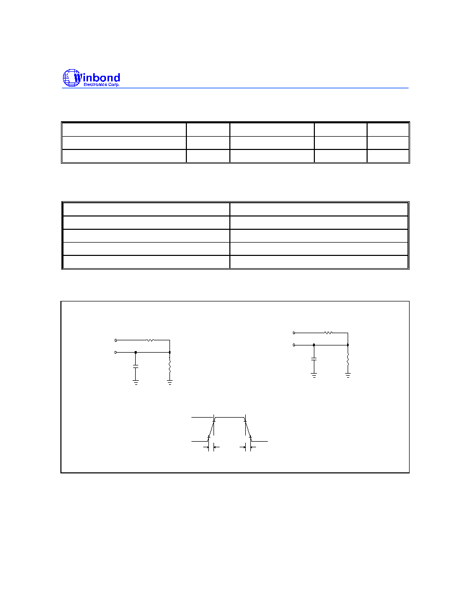
AC TEST LOADS AND WAVEFORM
90%
90%
3 nS
10%
3 nS
10%
R1 320 ohm
3.3V
OUTPUT
R2
350 ohm
30 pF
Including
Jig and
Scope
3.0V
0V
3.3V
OUTPUT
R1 320 ohm
5 pF
Including
Jig and
Scope
R2
350 ohm
(For T
CLZ1,
CLZ2,
OLZ,
CHZ1,
CHZ2,
OHZ,
WHZ,
OW
T
T
T
T
T
T
T
)
Preliminary W24L01A
- 4 -
AC CHARACTERISTICS
(V
DD
= 3.3V
±
5%, V
SS
= 0V, T
A
= 0 to 70
∞
C for 10/12/15 nS ; -20 to 85
∞
C for 12/15 nS)
Read Cycle
PARAMETER
SYM.
W24L01A-10 W24L01A-12
W24L01A-15 UNIT
MIN. MAX. MIN. MAX. MIN. MAX.
Read Cycle Time
T
RC
10
-
12
-
15
-
nS
Address Access Time
T
AA
-
10
-
12
-
15
nS
Chip Select Access Time
T
ACS
-
10
-
12
-
15
nS
Output Enable to Output Valid
T
AOE
-
5
-
6
-
7
nS
Chip Selection to Output in Low Z
T
CLZ*
3
-
3
-
3
-
nS
Output Enable to Output in Low Z
T
OLZ*
0
-
0
-
0
-
nS
Chip Deselection to Output in High Z
T
CHZ*
-
5
-
6
-
7
nS
Output Disable to Output in High Z
T
OHZ*
-
5
-
6
-
7
nS
Output Hold from Address Change
T
OH
3
-
3
-
3
-
nS
*
These parameters are sampled but not 100% tested.
Write Cycle
W24L01A-10 W24L01A-12 W24L01A-15
PARAMETER
SYM.
MIN. MAX. MIN. MAX. MIN. MAX.
UNIT
Write Cycle Time
T
WC
10
-
12
-
15
-
nS
Chip Selection to End of Write
T
CW1
9
-
10
-
13
nS
Address Valid to End of Write
T
AW
9
-
10
-
13
-
nS
Address Setup Time
T
AS
0
-
0
-
0
nS
Write Pulse Width
T
WP
9
-
10
-
10
-
nS
Write Recovery Time
CS
,
WE
T
WR
0
-
0
-
0
-
nS
Data Valid to End of Write
T
DW
5
-
7
-
9
-
nS
Data Hold from End of Write
T
DH
0
-
0
-
0
-
nS
Write to Output in High Z
T
WHZ
*
-
5
-
6
-
8
nS
Output Disable to Output in High Z
T
OHZ
*
-
5
-
6
-
8
nS
Output Active from End of Write
T
OW
0
-
0
-
0
-
nS
*
These parameters are sampled but not 100% tested.

Preliminary W24L01A
Publication Release Date: April 26, 2002
- 5 - Revision A1
TIMING WAVEFORMS
Read Cycle 1
(Address Controlled)
Address
T
T
T
T
D
OH
AA
RC
OH
OUT
Read Cycle 2
(Chip Select Controlled)
CS1
CS2
D
T
T
T
T
T
T
ACS1
ACS2
CLZ1
CLZ2
CHZ1
CHZ2
OUT
Read Cycle 3
(Output Enable Controlled)
Address
T
OE
CS1
CS2
D
T
T
T
T
T
T
T
T
T
T
T
OH
CHZ1
CHZ2
OHZ
AA
RC
AOE
CLZ1
ACS1
ACS2
CLZ2
OLZ
OUT

Preliminary W24L01A
- 6 -
Timing Waveforms, continued
Write Cycle 1
( OE
Clock)
Address
OE
CS1
CS2
WE
D
D
T
T
(1, 4)
OUT
IN
OHZ
WC
T
WR1
T
CW1
T
CW2
T
AW
T
WP
T
WR2
T
AS
T
DW
T
DH
Write Cycle 2
( OE
= V
IL
Fixed)
Address
CS1
CS2
WE
D
D
T
T
T
T
T
T
T
T
T
T
T
(2)
(3)
T
T
WC
CW1
WR1
CW2
AW
WP
WR2
OW
WHZ (1, 4)
DW
DH
OH
AS
OUT
IN
Notes:
1. During this period, I/O pins are in the output state, so input signals of opposite phase to the outputs should not be applied.
2. The data output from D
OUT
are the same as the data written to D
IN
during the write cycle.
3. Dout provides the read data for the next address.
4. Transition is measured
±
500 mV from steady state with C
L
= 5 pF. This parameter is guaranteed but not 100% tested.

Preliminary W24L01A
Publication Release Date: April 26, 2002
- 7 - Revision A1
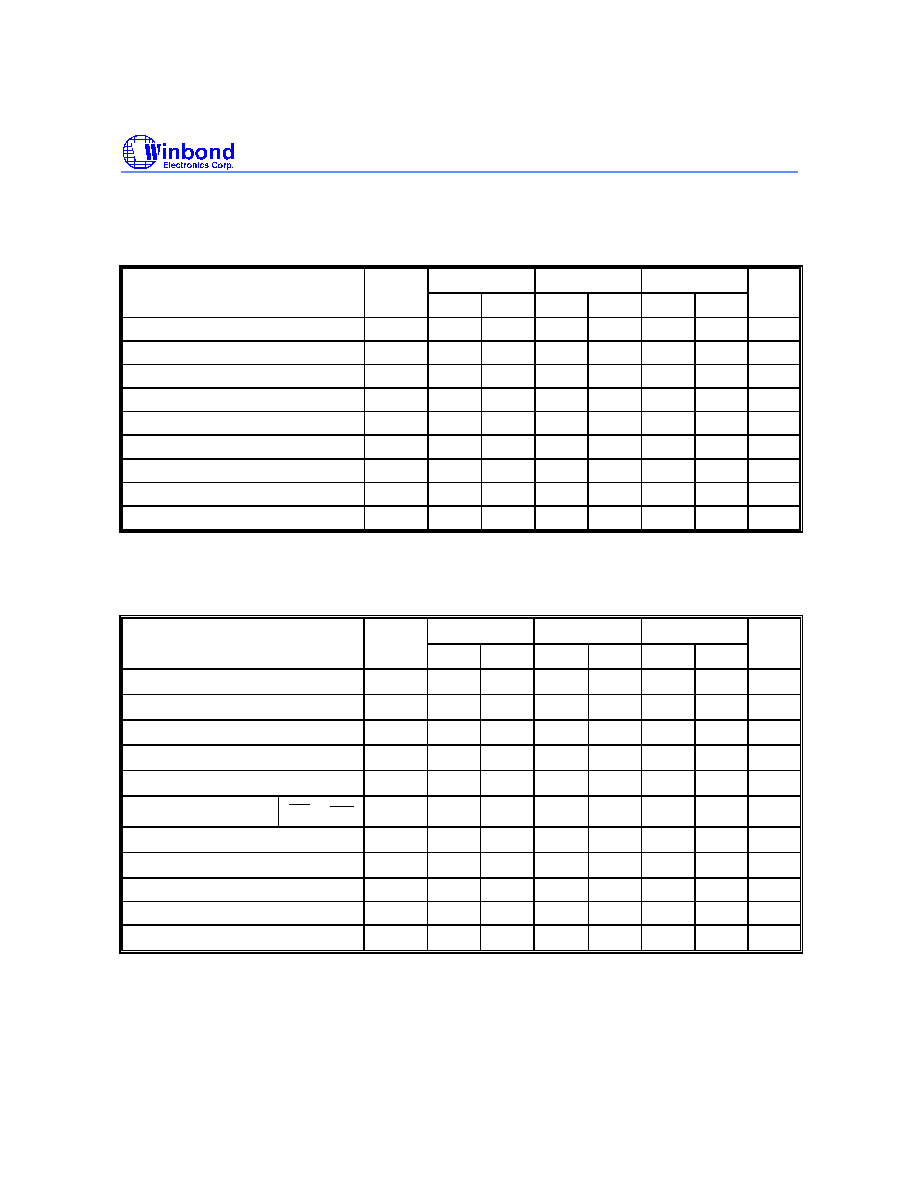
ORDERING INFORMATION
PART NO.
ACCESS
TIME
(nS)
OPERATING
CURRENT
Max. (mA)
STANDBY
CURRENT
Max. (mA)
OPERATION
TEMPERATURE
(
∞
C)
PACKAGE
W24L01AJ-10
10
130
5
0 to +70
300 mil SOJ
W24L01AJ-12
12
120
5
0 to +70
300 mil SOJ
W24L01AJ-15
15
100
5
0 to +70
300 mil SOJ
W24L01AQ-10
10
130
5
0 to +70
TSOPI (8 x 13.4 mm^2)
W24L01AQ-12
12
120
5
0 to +70
TSOPI (8 x 13.4 mm^2)
W24L01AQ-15
15
100
5
0 to +70
TSOPI(8 x 13.4 mm^2)
W24L01AT-10
10
130
5
0 to +70
TSOPI (8 x 20 mm^2)
W24L01AT-12
12
120
5
0 to +70
TSOPI (8 x 20 mm^2)
W24L01AT-15
15
100
5
0 to +70
TSOPI (8 x 20 mm^2)
W24L01AJ12E
12
120
5
-20 to +85
300 mil SOJ
W24L01AJ15E
15
100
5
-20 to +85
300 mil SOJ
W24L01AQ12E
12
120
5
-20 to +85
TSOPI (8 x 13.4 mm^2)
W24L01AQ15E
15
100
5
-20 to +85
TSOPI (8 x 13.4 mm^2)
W24L01AT12E
12
120
5
-20 to +85
TSOPI (8 x 20 mm^2)
W24L01AT15E
15
100
5
-20 to +85
TSOPI (8 x 20 mm^2)
Notes:
1. Winbond reserves the right to make changes to its products without prior notice.
2. Purchasers are responsible for performing appropriate quality assurance testing on products intended for use in applications
where personal injury might occur as a consequence of product failure.

Preliminary W24L01A
- 8 -
PACKAGE DIMENSIONS
32-pin SOJ
D
H
B
b
e
e
1
16
17
32
E
Y
A
A
A
Seating Plane
c
L
S
Symbol
Dimension in mm
Dimension in Inches
Min.
Nom.
Max.
Min.
Nom.
Max.
A
A
A
B
b
c
D
E
e
e
H
L
S
Y
0.140
0.020
0.095
0.100
0.105
0.032
0.028
0.026
0.022
0.018
0.016
0.014
0.010
0.008
0.835
0.825
0.305
0.300
0.295
0.056
0.050
0.044
0.287
0.267
0.247
0.345
0.335
0.325
0.080
0.045
0.004
0
10
0.815
3.556
0.508
2.413
2.540
2.667
0.813
0.711
0.660
0.559
0.457
0.406
0.356
0.254
0.203
21.209
20.955
7.747
7.620
7.493
1.422
1.270
1.118
7.290
6.782
6.274
8.763
8.509
8.255
2.032
1.143
0.102
0
∞
10
∞
20.701
__
__
__
__
__
__
__
__
__
__
__
__
__
__
__
__
__
__
__
__
__
__
1
2
1
e
e
1
2
1
32-Lead Small Type One TSOP (8 x 13.4)
A
A
A
2
1
L
L
1
Y
c
E
H
D
D
b
e
1
Controlling dimension: Millimeters
Min.
Dimension in mm
Nom. Max.
Min.
Nom.
Max.
Symbol
A
A
b
c
D
E
e
L
L
Y
1
1
2
A
H
D
11.70
13.20
0.675
1.25
0.05
0.15
1.05
1.00
0.95
0.17
0.14
0.30
0.00
0.20
0.27
0.15
0.16
11.80 11.90
13.40 13.60
0.50
0.50
0.70
0.10
0.049
0.006
0.041
0.039
0.037
0.007 0.008 0.009
0.0056 0.0059 0.0062
0.461
0.465 0.469
7.90
8.00
8.10
0.311 0.315 0.319
0.520 0.528 0.536
0.020
0.012 0.020 0.028
0.027
0.000
0.004
0
3
5
0
3
5
0.002
Dimension in Inches

Preliminary W24L01A
Publication Release Date: April 26, 2002
- 9 - Revision A1
Package Dimensions, continued
32-pin TSOP
A
A
A
2
1
L
L
1
Y
c
E
H
D
D
b
e
M
0.10(0.004)
Min.
Nom.
Max.
Min.
Nom.
Max.
Symbol
A
A
b
c
D
E
e
L
L
Y
1
1
2
A
H
D
Note:
Controlling dimension: Millimeter
Dimension in Inches
0.047
0.006
0.041
0.039
0.037
0.007
0.008
0.009
0.005
0.006
0.007
0.720
0.724
0.728
0.311
0.315
0.319
0.780
0.787
0.795
0.020
0.016
0.020
0.024
0.031
0.000
0.004
1
3
5
0.002
1.20
0.05
0.15
1.05
1.00
0.95
0.17
0.12
18.30
7.90
19.80
0.40
0.00
1
0.20
0.23
0.15
0.17
18.40
18.50
8.00
8.10
20.00
20.20
0.50
0.50
0.60
0.80
0.10
3
5
Dimension in mm
__
__
__
__
__
__
__
__
__
__
__
__
__
__
__
__

Preliminary W24L01A
- 10 -
VERSION HISTORY
VERSION
DATE
PAGE
DESCRIPTION
A1
Apr. 26, 2002
-
Initial Issued
Headquarters
No. 4, Creation Rd. III,
Science-Based Industrial Park,
Hsinchu, Taiwan
TEL: 886-3-5770066
FAX: 886-3-5665577
http://www.winbond.com.tw/
Taipei Office
TEL: 886-2-8177-7168
FAX: 886-2-8751-3579
Winbond Electronics Corporation America
2727 North First Street, San Jose,
CA 95134, U.S.A.
TEL: 1-408-9436666
FAX: 1-408-5441798
Winbond Electronics (H.K.) Ltd.
No. 378 Kwun Tong Rd.,
Kowloon, Hong Kong
FAX: 852-27552064
Unit 9-15, 22F, Millennium City,
TEL: 852-27513100
Please note that all data and specifications are subject to change without notice.
All the trade marks of products and companies mentioned in this data sheet belong to their respective owners.
Winbond Electronics (Shanghai) Ltd.
200336 China
FAX: 86-21-62365998
27F, 2299 Yan An W. Rd. Shanghai,
TEL: 86-21-62365999
Winbond Electronics Corporation Japan
Shinyokohama Kohoku-ku,
Yokohama, 222-0033
FAX: 81-45-4781800
7F Daini-ueno BLDG, 3-7-18
TEL: 81-45-4781881
9F, No.480, Rueiguang Rd.,
Neihu Chiu, Taipei, 114,
Taiwan, R.O.C.