 | –≠–ª–µ–∫—Ç—Ä–æ–Ω–Ω—ã–π –∫–æ–º–ø–æ–Ω–µ–Ω—Ç: W45B512P | –°–∫–∞—á–∞—Ç—å:  PDF PDF  ZIP ZIP |

Preliminary W45B512
512K
◊
1 SERIAL FLASH
Publication Release Date: February 21, 2002
- 1 - Revision A1
GENERAL DESCRIPTION
The W45B512 is manufactured with Winbond's high performance CMOS WinFlash technology. The
Serial Flash is organized as 16 sectors of 4096 Bytes for the W45B512. The memory is accessed for
Read or Erase/Program by the SPI bus compatible serial protocol. The bus signals are: serial data
input (SI), serial data output (SO), serial clock (SCK), write protect (#WP), chip enable (#CE), and
hardware reset (#RESET). This device is offered in 8L SON and 32L PLCC package.
FEATURES
∑
Single 2.7
-
3.6V Read and Write Operations
∑
Serial Interface Architecture
-
SPI Compatible: Mode 0 and Mode 3
∑
Byte Serial Read with Single Command
∑
Superior Reliability
-
Endurance: 10,000 Cycles (Typ.)
-
20 years Data Retention
∑
Low Power Consumption
-
Active Current: 30 mA (Max.)
-
Standby Current: 15 µA (Max.)
∑
Sector or Chip-erase Capability
-
Uniform 4 KByte sectors
∑
Fast Erase and Byte-program
-
Chip-erase Time: 100 mS (Max.)
-
Sector-erase Time: 25 mS (Max.)
-
Byte-program Time: 50 µS (Max.)
∑
Automatic Write Timing
-
Internal V
PP
Generation
∑
End-of-Write Detection
-
Software Status
∑
20 MHz Max Clock Frequency
∑
Hardware Reset Pin (#RESET)
-
Resets the device to Standby Mode
∑
TTL Compatibility
∑
Hardware Data Protection
-
Protects/Unprotects the device from Write
operation
∑
Packages Available
8L SON (5 x 6 mm), 32L PLCC

Preliminary W45B512
- 2 -
PIN CONFIGURATIONS
1
2
3
4
8
7
6
5
8L SON
Top View
VDD
#RESE
T
SCK
SI
#CE
SO
#WP
Vss
5
6
7
9
10
11
12
13
29
28
27
26
25
24
23
22
21
30
31
32
1
2
3
4
8
20
19
18
17
16
15
14
S
O
V
D
D
32L
PLCC
S
C
K
N
C
NC
NC
#WP
N
C
N
C
NC
NC
NC
NC
NC
NC
NC
#CE
N
C
V
S
S
N
C
N
C
N
C
N
C
NC
NC
NC
NC
NC
NC
#
R
E
S
E
T
SI
N
C
BLOCK DIAGRAM
SuperFlash
Cell Array
X-Decoder
Address
Buffers
and
Latches
Y-Decoder
Control Logic
I/O Buffers
and Data
Latches
Serial Interface
#CE SCK SI SO #WP #RESET
PIN DESCRIPTION
SYMBOL
PIN NAME
#CE
Chip Enable
SI
Serial Data Input
SO
Serial Data Output
SCK
Serial Clock
#WP
Write Protect
#RESET Reset
V
DD
Power Supply
V
SS
Ground
PRODUCT IDENTIFICATION
BYTE
DATA
Manufacturer's ID
0000
h
DA
h
Device ID: W45B512
0001
h
98
h

Preliminary W45B512
Publication Release Date: February 21, 2002
- 3 - Revision A1
FUNCTIONAL DESCRIPTION
Device Operation
The W45B512 uses bus cycles of 8 bits each for commands, data, and addresses to execute
operations. The operation instructions are listed in the table below. All instructions are synchronized off
a high to low transition of #CE. The first low to high transition on SCK will initiate the instruction
sequence. Inputs will be accepted on the rising edge of SCK starting with the most significant bit. Any
low to high transition on #CE before the input instruction completes will terminate any instruction in
progress and return the device to the standby mode.
Read
The Read operation outputs the data in order from the initial accessed address. While SCK is input,
the address will be incremented automatically until end (top) of the address space, then the internal
address pointer automatically increments to beginning (bottom) of the address space (00000h), and
data out stream will continue. The read data stream is continuous through all addresses until
terminated by a low to high transition on #CE.
Sector/Chip-erase Operation
The Sector-Erase operation clears all bits in the selected sector to "FF". The Chip -Erase instruction
clears all bits in the device to "FF".
Byte-program Operation
The Byte-Program operation programs the bits in the selected byte to the desired data. The selected
byte must be in the erased state ("FF") when initiating a Program operation. The data is input from bit 7
to bit 0 in order.
Software Status Operation
The Status operation determines if an Erase or Program operation is in progress. If bit 0 is at a "0" an
Erase or Program operation is in progress, the device is busy. If bit 0 is at a "1" the device is ready for
any valid operation. The status read is continuous with ongoing clock cycles until terminated by a low
to high transition on #CE.
Reset
Reset will terminate any operation, e.g., Read, Erase and Program, in progress. It is activated by a
high to low transition on the #RESET pin. The device will remain in reset condition as long as #RESET
is low. Minimum reset time is 10
µ
S. See Figure 14 for reset timing diagram. #RESET is internally
pulled-up and could remain unconnected during normal operation. After reset, the device is in standby
mode, a high to low transition on #CE is required to start the next operation. An internal power-on reset
circuit protects against accidental data writes. Applying a logic level low to #RESET during the power-
on process then changing to a logic level high when V
DD
has reached the correct voltage level will
provide additional protection against accidental writes during power on.
Read WINBOND ID/Read Device ID
The Read Manufacturer ID and Read Device ID operations read the JEDEC assigned manufacturer
identification and the manufacturer assigned device identification codes. These codes may be used to
determine the actual device resident in the system.
Preliminary W45B512
- 4 -
Write Protect
The #WP pin provides inadvertent write protection. The #WP pin must be held high for any Erase or
Program operation. The #WP pin is "don't care" for all other operations. In typical use, the #WP pin is
connected to V
SS
with a standard pull-down resistor. #WP is then driven high whenever an Erase or
Program operation is required. If the #WP pin is tied to V
DD
with a pull-up resistor, then all operations
may occur and the write protection feature is disabled. The #WP pin has an internal pull-up and could
remain unconnected when not used.
DEVICE OPERATION INSTRUCTION
BUS CYCLE
1
2
3
4
5
6
7
Operation/Type
Command Address
1
Address Address
Data
Dummy
Data
Read
FFh
A
23
-
A
16
A
15
-
A
8
A
7
-
A
0
X
X
Dout
Sector-erase
2
20h
A
23
-
A
16
A
15
-
A
8
X
Dout
X
Chip-erase
60h
X
X
X
Dout
X
Byte-program
10h
A
23
-
A
16
A
15
-
A
8
A
7
-
A
0
Din
X
Software-status
9Fh
Dout
Read Manufacture
ID
90h
X
X
A
0
=
0
DAh
Read Device ID
3
90h
X
X
A
0
=
1
98h
Notes:
1. A23
-
A16 are "Don't Care" for device.
2. A15
-
A12 are used to determine sector address, A11
-
A8 are don't care.
3. With A15
-
A1 = 0, W45B512 Device ID = 98h, is read with A0 = 1.
DEVICE OPERATION TABLE
OPERATION
SI
SO
#CE
1
#WP
#RESET
Read
X
Dout
Low
X
High
Sector-erase
X
X
Low
High
High
Chip-erase
X
X
Low
High
High
Byte-program
Din
X
Low
High
High
Software-status
X
Dout
Low
X
High
Reset2
X
X
X
X
Low
Read Manufacture ID
X
Dout
Low
X
High
Read Device ID
X
Dout
Low
X
High
Notes:
1. A high to low transition on #CE will be required to start any device operation except for Reset.
2. The #RESET low will return the device to standby and terminate any Erase or Program operation in progress.

Preliminary W45B512
Publication Release Date: February 21, 2002
- 5 - Revision A1
DC CHARACTERISTICS
Absolute Maximum Stress Ratings
(Applied conditions greater than those listed under "Absolute maximum Stress Ratings" may cause
permanent damage to the device. This is a stress rating only and functional operation of the device at
these conditions or conditions greater than those defined in the operational sections of this data sheet
is not implied. Exposure to absolute maximum stress rating conditions may affect device reliability.)
PARAMETER
RATING
UNIT
Temperature Under Bias
-55 to +125
∞C
Storage Temperature
-65 to +150
∞
C
D. C. Voltage on Any Pin to Ground Potential
-0.5 to V
DD
+0.5
V
Transient Voltage (<20 nS) on Any Pin to Ground Potential
-1.0 to V
DD
+1.0
V
Package Power Dissipation Capability (T
A
= 25∞ C)
1.0
W
Surface Mount Lead Soldering Temperature (3 Seconds)
240
∞C
Output Short Circuit Current
1
50
mA
Note: Exposure to conditions beyond those listed under Absolute Maximum Ratings may adversely affect the life and reliability
of the device.
DC Operating Characteristics
(V
DD
=2.7V
-
3.6V, V
SS
= 0V, T
A
= 0 to 70
∞
C)
LIMITS
PARAMETER
SYM.
TEST CONDITION
MIN.
MAX. UNITS
Program/Erase
-
30
mA
Power Supply Current
I
DD
f = 20 MHz
#CE = V
IL,
V
DD
= V
DD
Max.
Read
-
20
mA
Standby Current
I
SB
#CE = V
IHC
, V
DD
= V
DD
Max.
-
15
µ
A
Input Leakage
Output Leakage
I
LI
I
LO
V
IN
= GND to V
DD
, V
DD
= V
DD
Max.
V
OUT
= GND to V
DD
, V
DD
= V
DD
Max.
-
2
2
µ
A
µ
A
Input Low Voltage
V
IL
-0.2
0.6
V
Input High Voltage
V
IH
2.0 V
DD
+0.3
V
Output Low Voltage
V
OL
I
OL
= 1.6 mA
-
0.4
V
Output High Voltage
V
OH
I
OH
= -0.4 mA
2.4
-
V
Note: Outputs shorted for no more than one second. No more than one output shorted at a time.

Preliminary W45B512
- 6 -
CAPACITANCE
(V
DD
= 2.7V ~ 3.6V, T
A
= 25
∞
C, f = 1 MHz)
PARAMETER
SYMBOL
CONDITIONS
MAX.
UNIT
Output Pin Capacitance
C
OUT1
V
DQ
= 0V
12
pF
Input Pin Capacitance
C
IN1
V
IN
= 0V
6
pF
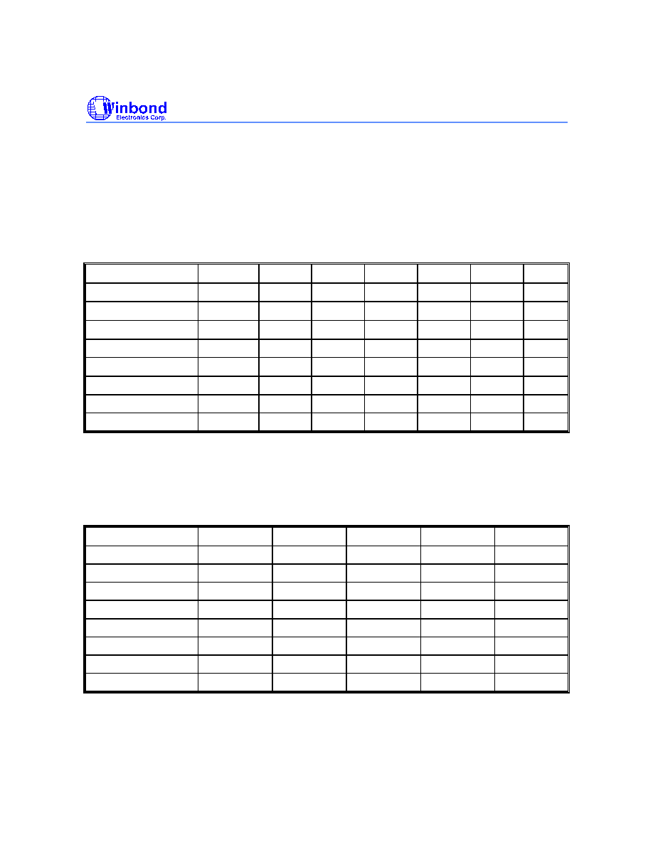
AC CHARACTERISTICS
AC Test Conditions
(V
DD
= 2.7V ~ 3.6V)
PARAMETER
CONDITIONS
Input Rise/Fall Time
<5 nS
Input/Output Timing Level
0.5 V
DD
/ 0.5 V
DD
Output Load
C
L
= 30 pF
AC Test Load and Waveform
CL =30pF
INPUT
REFERENCE POINTS
OUTPUT
V
IHT
V
ILT
VIT
V
OT
AC test inputs are driven at V
IHT
(0.9 V
DD
) for a logic "1" and V
ILT
(0.1 V
DD
) for a logic "0".Measurement reference points
for inputs and outputs are at V
IT
(0.5 V
DD
) and V
OT
(0.5 V
DD
) Input rise and fall times (10%
90%) are <5 nS.
Note: V
IT
: VINPUT Test; V
OT
: VOUTPUT Test; V
IHT
: VINPUT HIGH Test; V
ILT
; VINPUT LOW Test
Preliminary W45B512
Publication Release Date: February 21, 2002
- 7 - Revision A1
AC Operating Characteristics
(V
DD
= 2.7V ~ 3.6V)
LIMITS
PARAMETER
SYMBOL
MIN.
MAX.
UNITS
Serial Clock Frequency
F
CLK
20
MHz
Serial Clock High Time
T
SCKH
22
-
nS
Serial Clock Low Time
T
SCKL
22
-
nS
#CE Setup Time
T
CES
10
-
nS
#CE Hold Time
T
CEH
10
-
nS
#CE High Time
T
CPH
50
-
nS
#CE High to High-Z Output
T
CHZ
-
20
nS
#CE Low to Low-Z Output
T
CLZ
0
-
nS
#RESET Low to High-Z Output
T
RLZ
-
20
nS
Data In Setup Time
T
DS
5
-
nS
Data In Hold Time
T
DH
5
-
nS
Output Hold from SCK Change
T
OH
0
-
nS
Output Valid from SCK
T
V
-
25
nS
Write Protect Setup Time
T
WPS
10
-
nS
Write Protect Hold Time
T
WPH
10
-
nS
Sector-erase
T
SE
-
25
mS
Chip-erase
T
SCE
-
100
mS
Byte-program
T
BP
-
50
µ
S
Reset Pulse Width
T
RST
10
-
µ
S
Reset Recovery Time
T
REC
-
1
µ
S
Reset Time After Power-up
T
PURST
10
-
µ
S

Preliminary W45B512
- 8 -
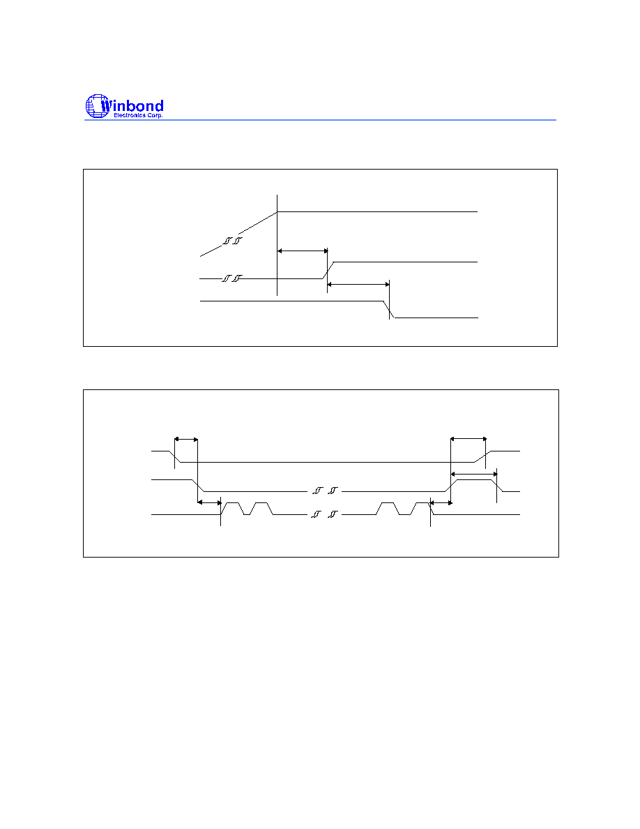
TIMING WAVEFORMS
Serial Input Timing Diagram (Inactive Serial Clock Low - Mode 0)
DATA VALID
HIGH-Z
HIGH-Z
T
CEH
T
CPH
T
CES
T
T
DS
DH
#WP
#CE
SCK
SI
SO
T
T
SCKH
SCKL
Serial Output Timing Diagram (Inactive Serial Clock Low - Mode 0)
DATA VALID
SCKH
T
SCKL
T
T
OH
T
CLZ
T
T
CEH
CHZ
#WP
#CE
SCK
SO
SI
T
V
Serial Input Timing Diagram (Inactive Serial Clock High - Mode 3)
CES
T
SCKH
SCKL
T
T
DS
DH
T
T
HIGH-Z
HIGH-Z
DATA VALID
CEH
T
CPH
T
#CE
SCK
SI
SO
#WP

Preliminary W45B512
Publication Release Date: February 21, 2002
- 9 - Revision A1
Timing Waveforms, continued
Serial Output Timing Diagram (Inactive Serial Clock High - Mode 3)
SCKH
T
SCKL
T
CLZ
T
DATA VALID
T
V
T
OH
T
T
CEH
CHZ
#WP
#CE
SCK
SO
SI
Sector-erase Timing Diagram
HIGH IMPEDANCE
ADD.
ADD.
X
X
D0H
0 0
0
0 0
0
0
1
0
1
2
3
4
5
6
7
8
15 16 23 24 31 32
39 40 47
T
WPH
T
WPS
SELF-TIMED SECTOR-
ERASE CYCLE
#WP
#CE
SCK
SI
SO
T
SE

Preliminary W45B512
- 10 -
Timing Waveforms, continued
Chip-erase Timing Diagram
#WP
#CE
SCK
SI
SO
HIGH IMPEDANCE
X
X
D0H
0
0
0 0
0
0
1
0
1
2
3
4
5
6
7
8
15 16 23 24 31 32
39 40 47
T
WPH
T
WPS
T
SCE
1
X
X
SELF-TIMED CHIP-
ERASE CYCLE
Byte-program Timing Diagram
HIGH IMPEDANCE
15
0
1
2
3
4
5
6
7
8
16 23 24 31 32
39 40 47
T
WPH
T
WPS
SELF-TIMED BYTE-
PROGRAM CYCLE
T
BP
#WP
#CE
SCK
SI
SO
X
Din
0
0 0
0
0
1
0 0
ADD.
ADD.
ADD.
MSB
LSB

Preliminary W45B512
Publication Release Date: February 21, 2002
- 11 - Revision A1
Timing Waveforms, continued
Read Timing Diagram
0
1
2
3
4
5
6
7
8
16 23 24 31
32
39 40
15
47
55
48
56
63 64
71
X
0
0 0
0
0
1
0 0
ADD.
ADD.
ADD.
X
HIGH IMPEDANCE
#WP
#CE
SCK
SI
SO
Dout
Dout
Dout
MSB
MSB
MSB
N
N+1
N+2
Read-Id Timing Diagram
0
1
2
3
4
5
6
7
8
16 23 24 31
32
39 40
15
47
55
48
56
6364
71
X
0 0
0
0
1
0 0
ADD
HIGH IMPEDANCE
#WP
#CE
SCK
SI
SO
Dout
MSB
LSB
1
X
1
Note: 1. Manufacturer's ID = DAh is read with A 0 = 0
Device ID = 98h is read with A 0 = 1

Preliminary W45B512
- 12 -
Timing Waveforms, continued
Software-Status Timing Diagram
0
1
2
3
4
5
6
7
8
11
13
14
24
10
1
0 0
HIGH IMPEDANCE
#WP
#CE
SCK
SI
SO
MSB
1
9
12
15 16
23
31
1 1 1 1
DATA
DATA
DATA
MSB
MSB
Reset Timing Diagram (Inactive Clock Polarity Low Shown)
HIGH IMPEDANCE
T
RLZ
T
T
T
REC
RST
CES
HIGH IMPEDANCE
#CE
SCK
SI
SO
#RESET
Preliminary W45B512
Publication Release Date: February 21, 2002
- 13 - Revision A1
Timing Waveforms, continued
Power-on Reset Timing Diagram
T
PURST
T
REC
V
DD
#RESET
#CE
Write Protect Timing Diagram
T
T
T
T
T
WPS
CES
WPH
CPH
CEH
#WP
#CE
SCK

Preliminary W45B512
- 14 -
ORDERING INFORMATION
PART NO. OPERATING
VOLTAGE
(V)
POWER
SUPPLY
CURRENT
MAX. (mA)
STANDBY
V
DD
CURRENT
MAX. (
µ
A)
PACKAGE
CYCLING OPERATING
TEMP.
(∞C)
W45B512Z
2.7V
-
3.6V
30
15
8L SON
(5 x 6 mm)
10K
0∞C
-
70∞C
W45B512P
2.7V
-
3.6V
30
15
32L PLCC
10K
0∞C
-
70∞C
Notes:
1. Winbond reserves the right to make changes to its products without prior notice.
2. Purchasers are responsible for performing appropriate quality assurance testing on products intended for use in
applications where personal injury might occur as a consequence of product failure.
HOW TO READ THE TOP MARKING
Example: The top marking of 32L-PLCC W45B512
1
st
line: winbond logo
2
nd
line: the part number: W45B512Z
3
rd
line: the lot number
4
th
line: the tracking code: 149 O B SA
149: Packages made in '01, week 49
O: Assembly house ID: A means ASE, O means OSE, ... etc.
B: IC revision; A means version A, H means version H, ... etc.
SA: Process code
W45B512Z
2138977A-A12
149OBSA

Preliminary W45B512
Publication Release Date: February 21, 2002
- 15 - Revision A1
PACKAGE DIMENSIONS
8L SON (5 x 6 mm)
32L PLCC
Notes:
L
c
1
b
2
A
H
E
E
e
b
D H
D
y
A
A
1
Seating Plane
E
G
G
D
1
13
14
20
29
32
4
5
21
30
1. Dimensions D & E do not include interlead flash.
2. Dimension b1 does not include dambar protrusion/intrusion.
3. Controlling dimension: Inches
4. General appearance spec. should be based on final
visual inspection sepc.
Symbol
Min.
Nom.
Max.
Max.
Nom.
Min.
Dimension in Inches
Dimension in mm
A
b
c
D
e
H
E
L
y
A
A
1
2
E
b
1
G
D
3.56
0.50
2.80
2.67
2.93
0.71
0.66
0.81
0.41
0.46
0.56
0.20
0.25
0.35
13.89
13.97
14.05
11.35
11.43
11.51
1.27
H
D
G
E
12.45
12.95
13.46
9.91
10.41
10.92
14.86
14.99
15.11
12.32
12.45
12.57
1.91
2.29
0.004
0.095
0.090
0.075
0.495
0.490
0.485
0.595
0.590
0.585
0.430
0.410
0.390
0.530
0.510
0.490
0.050
0.453
0.450
0.447
0.553
0.550
0.547
0.014
0.010
0.008
0.022
0.018
0.016
0.032
0.026
0.028
0.115
0.105
0.110
0.020
0.140
1.12
1.42
0.044
0.056
0
∞
10
∞
10
∞
0
∞
0.10
2.41

Preliminary W45B512
- 16 -
VERSION HISTORY
VERSION
DATE
PAGE
DESCRIPTION
A1
Feb. 21, 2002
-
Initial Issued
Headquarters
No. 4, Creation Rd. III,
Science-Based Industrial Park,
Hsinchu, Taiwan
TEL: 886-3-5770066
FAX: 886-3-5665577
http://www.winbond.com.tw/
Taipei Office
TEL: 886-2-8177-7168
FAX: 886-2-8751-3579
Winbond Electronics Corporation America
2727 North First Street, San Jose,
CA 95134, U.S.A.
TEL: 1-408-9436666
FAX: 1-408-5441798
Winbond Electronics (H.K.) Ltd.
No. 378 Kwun Tong Rd.,
Kowloon, Hong Kong
FAX: 852-27552064
Unit 9-15, 22F, Millennium City,
TEL: 852-27513100
Please note that all data and specifications are subject to change without notice.
All the trade marks of products and companies mentioned in this data sheet belong to their respective owners.
Winbond Electronics (Shanghai) Ltd.
200336 China
FAX: 86-21-62365998
27F, 2299 Yan An W. Rd. Shanghai,
TEL: 86-21-62365999
Winbond Electronics Corporation Japan
Shinyokohama Kohoku-ku,
Yokohama, 222-0033
FAX: 81-45-4781800
7F Daini-ueno BLDG, 3-7-18
TEL: 81-45-4781881
9F, No.480, Rueiguang Rd.,
Neihu Chiu, Taipei, 114,
Taiwan, R.O.C.