 | –≠–ª–µ–∫—Ç—Ä–æ–Ω–Ω—ã–π –∫–æ–º–ø–æ–Ω–µ–Ω—Ç: W51300 | –°–∫–∞—á–∞—Ç—å:  PDF PDF  ZIP ZIP |

W51300
FLASH VR CONTROLLER
Publication Release Date: April 1997
- 1 -
Revision A2
GENERAL DESCRIPTION
The W51300 is a voice recorder IC which contains A/D and D/A converters to digitize and reproduce
voice signals. An anti-alias/smoothing filter, AGC circuit, MIC preamplifier, and speaker power
amplifier are used to smooth the input voice and set the output voice to a certain volume while
minimizing the number of extra components needed. The recording time depends on the size of the
external memory.
The external memory is a nonvolatile flash EPROM that stores the voice data while power is switched
off. This external memory provides a great advantage in cartridge or greeting card applications. A
maximum of 16 Mbit of memory can be cascaded. In addition, the W51300's flexible segmentation,
selective recording/erasing, forward and backward move functions, and MCU interface provide
flexibility to meet the needs of a wide variety of applications.
FEATURES
∑
Modified ADM algorithm with 24 KHz sampling frequency when R
OSC
= 620 K
∑
Operates with Winbond serial flash EPROM
∑
Built-in A/D, D/A, MIC preamplifier, AGC circuit, anti-alias/smoothing filter, speaker power amplifier,
and LED indicator
∑
8 input trigger pins (L_REC, E_PLAY, L_PLAY, FWD, BWD, STOP, ERASE, RESET) debounced
to ensure noise-free operations
∑
Single/multi-voice segment operation, normal/CPU mode selected by pin option (SMODE, CPU)
∑
Cascadable for longer duration by directly cascading serial flash EPROMs (maximum 16 Mbits)
∑
Maximum 63 voice segments available in multi-segment operation
∑
Provides selective record, erase, and playback functions
∑
Provides low power detection circuit at 3.0V
∑
Provides both speaker direct drive and speaker current output (5 mA)
∑
Low power consumption:
-
Operating: 15 mA (typ.)
-
Standby: 0.01
µ
A (typ.)

W51300
- 2 -
PIN CONFIGURATION
1
2
3
4
5
6
7
8
9
10
11
12
13
16
14
15
24
25
26
27
28
20
21
22
23
17
18
19
32
31
30
29
TEST
AGC
BWD
STOP
EOP
FWD
RESET
VCCD
CLK
EXTCLK
MICREF
MIC
OSC
AUD
VSSD
VSSA
SPK+
SPK-
VCCA
ADDR
BUSY
LED
DATA
CTRL
MODE
CPU
SMODE
L_REC
L_PLAY
E_PLAY
ERASE
VCCA
PIN DESCRIPTION
NO.
PIN
I/O
DESCRIPTION
1
BWD
I/O
Message backward control pin in normal mode
Output clock signal (to MCU) in CPU mode
2
STOP
I
Stop playback control pin in normal mode
Input clock signal (from MCU) in CPU mode
3
EOP
I
End of page process signal (from flash EPROM)
4
CLK
O
Data clock pin for flash EPROM
5
ADDR
O
Address clock pin for flash EPROM
6
DATA
I/O
Bidirectional data pin for flash EPROM
7
CTRL
O
Control signal for flash EPROM
8
MODE
O
Mode control pin for flash EPROM

W51300
Publication Release Date: April 1997
- 3 -
Revision A2
Pin Description, continued
NO.
PIN
I/O
DESCRIPTION
9
BUSY
O
Output busy signal, HIGH during playback
10
LED
O
Blink (Flash (volume-controlled) during playback
Flash Blink (3 Hz) when during low battery is low, segment full, or
memory full
ON during recording, erasing, and memory formatting
11
V
SSD
-
Digital negative power supply
12
V
SSA
-
Analog negative power supply
13
SPK-
O
Speaker voltage output -
14
SPK+
O
Speaker voltage output +
15
V
CCA
-
Analog positive power supply
16
AUD
O
Speaker current output (maximum 5 mA when V
CC
= 4.5V)
17
V
CCA
-
Analog positive power supply +
18
OSC
I
Oscillation frequency control pin
19
MICREF
I
Microphone reference
20
MIC
I
Microphone input
21
AGC
I
Automatic gain control input
22
V
CCD
-
Digital positive power supply
23
CPU
I
Normal/CPU mode select pin: low for normal, high for CPU
24
SMODE
I
Multi/single segment select pin: low for multi, high for single
25
TEST
I
External test pin for testing
26
EXTCLK
I
External clock pin for testing
27
RESET
I
Reset control pin
28
L_REC
I
Level record control pin
29
L_PLAY
I
Level playback control pin
30
E_PLAY
I
Edge playback control pin
31
ERASE
I
Message erase control pin in normal mode
Input level signal (from MCU) in CPU mode
32
FWD
I/O
Message forward control pin in normal mode
Output level signal (to MCU) in CPU mode

W51300
- 4 -
BLOCK DIAGRAM
AGC
Amp
Anti-alias/
Smoothing
Filter
ADM
Modulator
Power
Amp
Logic/Timing Controller
MIC
MICREF
AGC
SPK+
SPK-
Flash EEPROM
Interface
DATA
CLK
ADDR
EOP
CTRL
MODE
SMODE
CPU
AUD
AUD
Amp
BUSY
VCCD
VSSD
VCCA
VSSA
L_REC
L_PLAY
RESET
LED
OSC
TEST
EXTCLK
E_PLAY
ERASE
STOP
FWD
BWD
MCU Interface
FUNCTIONAL DESCRIPTION
1. Single/Multi-segment Operation
The W51300 is typically used for either single or multi-segment operations. Single or multi-segment
operating mode is selected by pin option.
Single Segment
The SMODE pin should be connected to V
CC
. In this mode, only one voice segment can be recorded.
The storage duration can be extended by cascading serial flash EPROMs; up to 16 Mbits of memory
can be cascaded.
Multi-segment
The SMODE pin should be connected to V
SS
or left floating. In this mode, a maximum of 63 voice
segments can be recorded into flash EPROMs; up to 16 Mbits of memory can be cascaded.
Messages can easily be accessed by using the FWD, BWD, and PLAY pins.
2. Selective Record
When the system is operated in multi-segment mode, voice segments can be recorded selectively.
Users can insert a voice segment between any two existing voice segments. For instance, suppose
there are already five voice segments, 1, 2, 3, 4, and 5, and the CAP (current address/message
pointer) is at 3. Then a newly recorded voice segment will be assigned the number 4, and the original
segments 4 and 5 will be changed to 5 and 6, respectively. If the maximum number of voice
segments (63) or the end of memory space has been reached, a press of L_REC will be invalid and
the LED will flash at 3 Hz for 2 seconds to indicate the invalid action.

W51300
Publication Release Date: April 1997
- 5 -
Revision A2
3. Selective Erase
When the system is operated in multi-segment mode, voice segments can be erased selectively
instead of sequentially. Users can play the voice segments one by one until they reach the segment
to be erased, and then stop playing and press the ERASE key. The current voice segment will be
erased and the CAP value will be changed to the previous voice segment. The LED will light during
the erasing procedure to indicate that the system is busy, and all input triggers will be disabled except
for RESET.
4. Chip Erase
Pressing and holding the RESET key for more than two seconds will clear all data in the flash
EPROM.
5. Function Keys
In normal mode, eight input trigger pins with built-in debounce circuitry are used to operate the
W51300. These eight pins are described below.
L_REC
L_REC is an active-high, level-triggered recording pin with an internal 500 K
pull-low resistor. When
this pin goes high, the device starts recording and continues until this pin is released or the end of the
memory space is reached. When the memory or segment is full, this pin is invalid.
E_PLAY
E_PLAY is an active-high, edge-triggered playback pin with an internal 500 K
pull-low resistor. In
single segment operation, the toggle stop function is enabled. This means a debounced rising edge
on E_PLAY during voice playing will stop the ongoing playback operation immediately. In multi-
segment operation, the toggle skip function is enabled. This means a debounced rising edge on
E_PLAY during voice playing will cause the device to skip to the next voice segment. A rising edge
on this pin while the last voice segment is being played will cause the device to skip to the first voice
segment. This function is useful for fast scanning through a series of messages.
L_ PLAY
L_PLAY is an active-high, level-triggered playback pin with an internal 500 K
pull-low resistor. The
current voice segment will be played back when this pin is pressed. A concatenated loop playing
function is enabled to link all messages in a row and loop back to the first message when the last
message is reached.
STOP
This is an active-high, edge-triggered stop pin with an internal 500 K
pull-low resistor. Pressing this
pin immediately stops playback of the ongoing message. This pin is enabled only while a voice is
playing.
ERASE
ERASE is an active-high, edge-triggered erase pin with an internal 500 K
pull-low resistor. Pressing
this pin erases the current voice segment without affecting the content of the other segments.
FWD
This is an active-high, edge-triggered forward pin with an internal 500 K
pull-low resistor. Pressing
this pin for less than 1 second moves the CAP from the current voice segment to the next one.
Pressing this pin for more than 1 second moves the CAP from the current voice segment to the last
one.
W51300
- 6 -
BWD
This is an active-high, edge-triggered backward pin with an internal 500 K
pull-low resistor. Pressing
this pin for less than 1 second moves the CAP from the current voice segment to the previous one.
Pressing this pin for more than 1 second moves the CAP from the current voice segment to the first
one.
RESET
This is an active-high, edge-triggered reset pin with an internal 500 K
pull-low resistor. Pressing this
pin for less than 2 seconds causes the system power-on initialization procedure to be executed and
resets the message pointer to 1. Pressing this pin for more than 2 seconds executes the chip erase
procedure, so that all of the recorded messages are cleared.
6. Low Battery Warning
A low battery warning function is provided to protect the recorded voice messages from being lost
due to loss of power. Before a recording, erasing, or reset operation, the battery voltage will be
checked. If the voltage falls to 3
volts or below, all operations except the LED stop, and the LED
flashes at 3 Hz for 2 seconds to indicate that the battery is low.
7. Speaker Output
The W51300 provides two types of speaker drivers, direct drive and current output. The direct drive is
a voltage output from the built-in power amplifier. This output can be used to drive a speaker directly
without any extra components, such as resistors or transistors. The maximum driving current is 56
mA (rms) when the output is connected to a 16
speaker. The current output is the same as that of
the standard speaker driver used in most Winbond
PowerSpeech
TM
chips. The maximum driving
current is 5 mA when V
CC
= 4.5V.
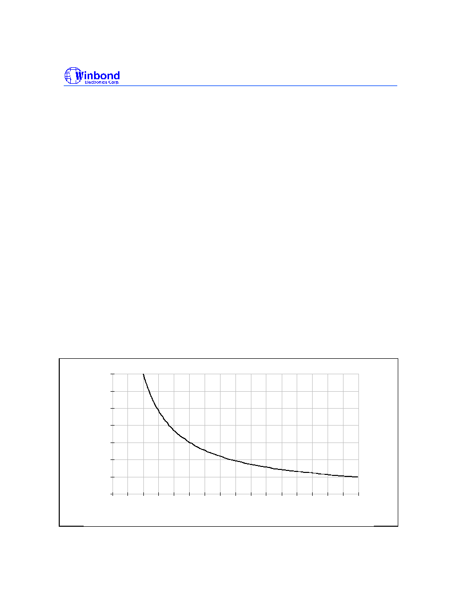
8. Sampling Frequency Adjustment
The external R
OSC
can be adjusted to change the system clock (F
OSC
) and sampling frequency (Fs).
The relationship between F
OSC
and Fs is Fs = F
OSC
/32. The relationship between Fs and R
OSC
is
shown is the figure below.
0
5
10
15
20
25
30
35
0
200
400
600
800 1,000 1,200 1,400 1,600 1,800 2,000 2,200 2,400 2,600 2,800 3,000 3,200
Rosc (KOhm)
Fs (KHz)

W51300
Publication Release Date: April 1997
- 7 -
Revision A2
9. MCU Interface
In CPU mode, five pins can be used as an MCU interface to communicate with external micro-
controllers by the counter method. RESET, ERASE, STOP are configured as input pins, while FWD
and BWD are configured as output pins. The application diagram is shown below.
Pin 1
Pin 2
Pin 3
Pin 4
ERASE
STOP
FWD
BWD
Microcontroller
W51300
Pin 0
RESET
The W51300 offers 10 operating modes that can be controlled by a microcontroller. The rising edge
of pin 1 informs the W51300 to begin to count the pulses generated on pin 2, and the falling edge of
pin 1 informs the W51300 to latch the pulse number. Then the number of pulses is decoded to
instruct the W51300 to perform various operations. The operating modes and the corresponding
waveforms are shown below.
. . .
T
T1
Pin 1
Pin 2
Note: T is 5
µ
S minimum at F
OSC
= 768 KHz.
T1 is 10
µ
S minimum at F
OSC
= 768 KHz.
ITEM
MODE NAME
NUMBER OF PULSES ON PIN 2
1
Record
1
2
Play
2
3
Erase
3
4
Stop (for record and play)
4
5
Memory Reset
5
6
System Reset
6
7
Read CAP (Current Address Pointer)
7
W51300
- 8 -
Continued
ITEM
MODE NAME
NUMBER OF PULSES ON PIN 2
8
Read ASN (Available Segment Number)
8
9
Store 4 Bytes Data to Flash EPROM
9
10
Read 4 Bytes Data from Flash EPROM
10
After receiving a command from the microcontroller, the W51300 will send back a corresponding
response, as shown below.
. . .
T1
T1
T1
Pin 3
Pin 4
Note: T1 is 5 msec at F
OSC
= 768 KHz.
ITEM
MODE NAME
NUMBER OF PULSES GENERATED ON PIN 4
1
Accept
0
2
Error: Low Battery
1
3
Error: Memory Full
2
4
Error: Out of Segments
3
5
Error: Wrong CAP
4
6
Unknown Mode
5
7
Unknown Error
6
When pin 3 is low and pin 4 is high, the W51300 is busy.
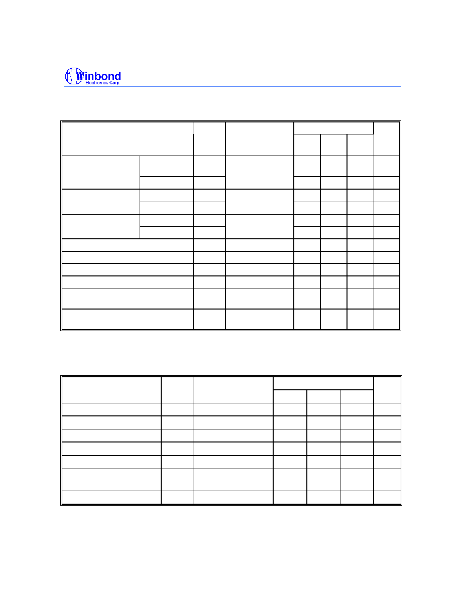
ABSOLUTE MAXIMUM RATINGS
PARAMETER
SYMBOL
CONDITION
RATED VALUE
UNIT
Operating Temp.
T
OPR
-
0 to +70
∞
C
Storage Temp.
T
STG
-
-55 to +150
∞
C
Power Supply
V
CC
-
V
SS
-
-0.3 to +7.0
V
Input DC Voltage
V
IN
All pins
V
SS
-0.3 to V
CC
+0.3
V
Note: Exposure to conditions beyond those listed under Absolute Maximum Ratings may adversely affect the life and reliability
of the device.

W51300
Publication Release Date: April 1997
- 9 -
Revision A2
DC CHARACTERISTICS
(V
CC
= 5V, V
CC
= 0V, T
A
= 25
∞
C)
PARAMETER
SYM.
CONDITIONS
LIMITS
UNIT
MIN.
TYP.
MAX.
Operating Voltage
V
CC
-
3.0
4.5
5.5
V
Standby Current
I
SB
All inputs =
GND
Data = 5V
0
0.01
1
µ
A
Operating Current
I
OP
No load
-
15
25
mA
Input Voltage
High
V
IH
All input pins
2.0
-
-
V
Low
V
IL
-
-
0.8
V
Input Low Current
I
IL
V
IN
= 0V
0
-
1
µ
A
Input High Current
Digital pins
I
IH1
V
IN
= 5V
5
8
12
µ
A
Analog
pins, MIC
I
IH2
V
IN
= 5V
0.8
1
1.2
mA
SMODE,
CPU
I
IH3
V
IN
= 5V
-
-
1
µ
A
TEST,
EXTCLK
I
IH4
V
IN
= 5V
50
75
100
µ
A
Output Low Current
ADDR,
CLK,
MODE,
CTRL,
DATA
I
OL1
V
Out
= 0.5V
0.5
1.5
3
mA
LED, BUSY
I
OL2
V
Out
= 0.5V
6
10
15
mA
Output High Current
ADDR,
CLK,
MODE,
CTRL,
DATA
I
OH1
V
Out
= 4.5V
-0.5
-1.5
-3
mA
LED, BUSY
I
OH2
V
Out
= 4.5V
-2.5
-4.5
-6.5
mA
Oscillation Frequency
F
OSC
R
OSC
= 620 K
610
768
920
KHz
W51300
- 10 -
AC CHARACTERISTICS
(V
CC
= 5V, V
CCS
= 0V, T
A
= 25
∞
C)
PARAMETER
SYM.
CONDITIONS
LIMITS
UNIT
MIN.
TYP. MAX
.
Input Debounce
Time
Normal
mode
T
DEB1
F
OSC
= 768 KHz
21
32
42.7
mS
CPU mode
T
DEB2
1.27
1.9
2.54
µ
S
CLK Duty Cycle
Write
T
CLK1
-
-
50
-
%
Read
T
CLK2
-
-
75
-
%
CLK Frequency
Write
F
CLK1
F
OSC
= 768 KHz
-
384
-
KHz
Read
F
CLK2
-
192
-
KHz
ADDR Duty Cycle
T
ADDR
-
-
50
-
%
ADDR Frequency
F
ADDR
F
OSC
= 768 KHz
-
384
-
KHz
Input Clock Duty Cycle of Erase Pin
T
IN
CPU mode
40
-
60
%
Input Clock Frequency of Erase Pin
F
IN
CPU mode
-
-
100
KHz
Output Clock Duty Cycle of BWD
Pin
T
OUT
CPU mode
-
50
-
%
Output Clock Frequency of BWD Pin
F
OUT
CPU mode,
F
OSC
= 768 KHz
-
100
Hz
ANALOG CIRCUIT CHARACTERISTICS
(V
CC
= 5V, V
SS
= 0V, T
A
= 25
∞
C)
PARAMETER
SYM.
CONDITIONS
LIMITS
UNIT
MIN.
TYP.
MAX.
MIC Input Voltage
V
MIC
Peak to Peak
-
-
20
mV
MIC Input Resistance
R
MIC
-
-
10
-
K
Passband of LPF
BW
F
OSC
= 768 KHz
-
3.5
-
KHz
Speaker Output Power
P
OUT
R
EXT
= 16
, rms
-
-
50
mW
Speaker Voltage Output
V
OUT
R
EXT
= 600
-
-
1.2
V
P-P
Speaker Current Output
I
AUD
V
CC
= 4.5V,
R
L
= 100
-4.0
-5.0
-6.0
mA
Speaker Resistance
R
SP
-
8
16
-

W51300
Publication Release Date: April 1997
- 11 -
Revision A2
TYPICAL APPLICATION CIRCUIT
(for reference only)
L_REC
E_PLAY
OSC
VCCD
VCCA
VSSD
VSSA
SPK+
SPK-
MIC
MICREF
AGC
8/16
SPEAKER
V
Rosc
MIC
C1
R1
C3
C4
W51300
R2
R3
C2
DATA
CTRL
CLK
ADDR
EOP
MODE
Vcc
V
W55Fxx
DATA
CTRL
CLK
ADDR
EOP
MODE
ERASE
RESET
LED
R4
SMODE
CPU
Component List:
R2 = 1 K
R1 = 470 K
R3 = 8.2 K
R4 = 220
C2 = 2.2 F
C3 = C4 = 0.22 F
µ
µ
Rosc = 620 K
C1 = 4.7 F
µ
FWD
BWD
L_PLAY
STOP
Cd
SS
DD
Cd
R5
R5 = 5.1 K
Cd = 0.1 F
µ
Notes:
1. R1 and C1 can be adjusted for different AGC attack time and release time.
2. Set C3 = C4 to reduce ground noise.

W51300
- 12 -
Headquarters
No. 4, Creation Rd. III,
Science-Based Industrial Park,
Hsinchu, Taiwan
TEL: 886-3-5770066
FAX: 886-3-5792697
http://www.winbond.com.tw/
Voice & Fax-on-demand: 886-2-7197006
Taipei Office
11F, No. 115, Sec. 3, Min-Sheng East Rd.,
Taipei, Taiwan
TEL: 886-2-7190505
FAX: 886-2-7197502
Winbond Electronics (H.K.) Ltd.
Rm. 803, World Trade Square, Tower II,
123 Hoi Bun Rd., Kwun Tong,
Kowloon, Hong Kong
TEL: 852-27516023
FAX: 852-27552064
Winbond Electronics North America Corp.
Winbond Memory Lab.
Winbond Microelectronics Corp.
Winbond Systems Lab.
2730 Orchard Parkway, San Jose,
CA 95134, U.S.A.
TEL: 1-408-9436666
FAX: 1-408-9436668
Note: All data and specifications are subject to change without notice.