
W522AXXX Data Sheet
PWM SYNTHESIZER
Publication Release Date: June 3, 2003
- 1 -
Revision A2
Table of Contents-
1.
GENERAL DESCRIPTION ............................................................................................................ 2
2.
FEATURES.................................................................................................................................... 2
3.
PIN DESCRIPTION ....................................................................................................................... 3
4.
BLOCK DIAGRAM ......................................................................................................................... 4
5.
ABSOLUTE MAXIMUM RATINGS ................................................................................................ 4
6.
ELECTRICAL CHARACTERISTICS.............................................................................................. 5
7.
APPLICATION CIRCUIT ............................................................................................................... 6
8.
REVISION HISTORY..................................................................................................................... 7
W522AXXX
- 2 -
1. GENERAL DESCRIPTION
W522AXXX is a synthesis IC that utilizes the 8-bit PCM coding method to generate high quality voice
effects. In order to save power, the W522AXXX provides PWM output to drive speaker directly without
extra transistor and resistor.
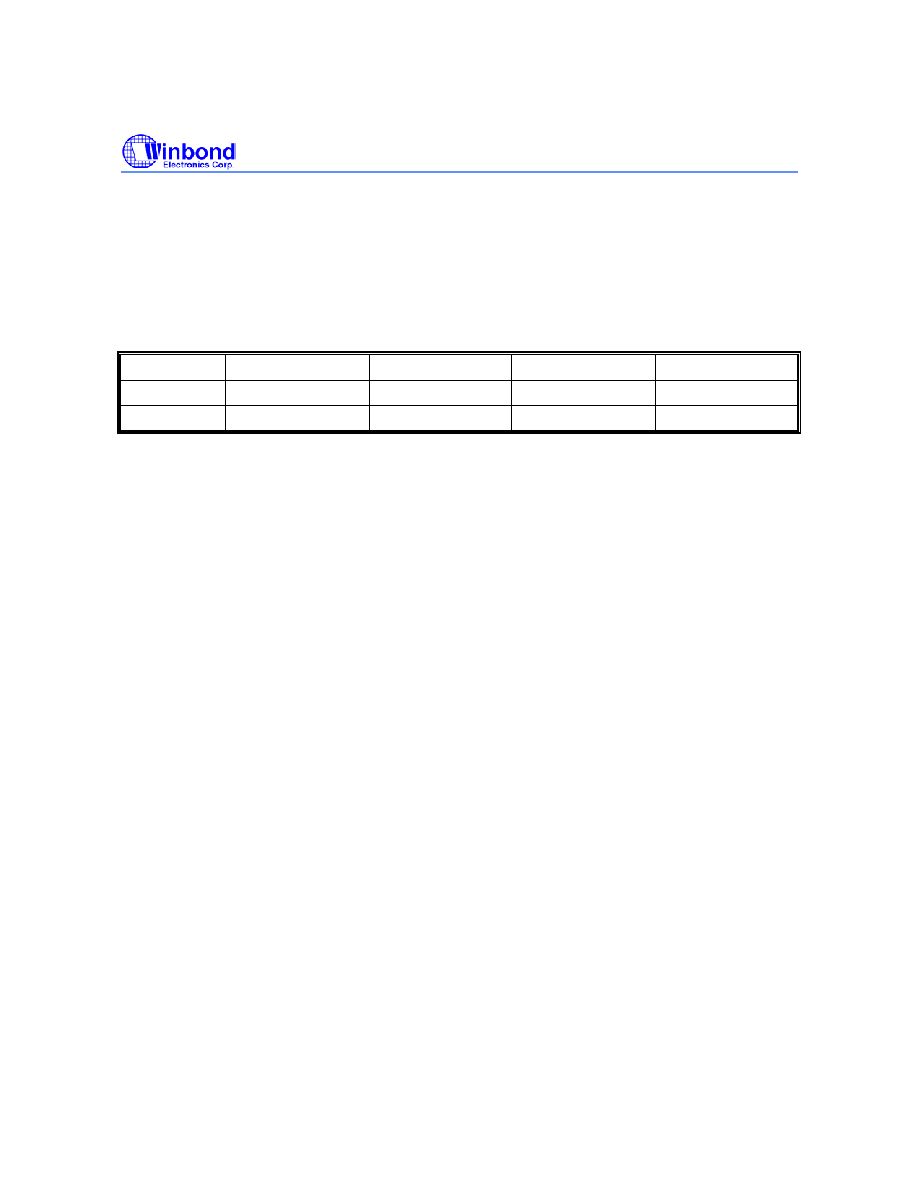
The W522AXXX's part number and corresponding duration time at various sampling rate listed as
below:
Part number
Duration @ 4KHz Duration @ 4.8KHz
Duration @ 6KHz
Duration @ 8KHz
W522A008
12.00 seconds
10.00 seconds
8.00 seconds
6.00 seconds
W522A010
16.00 seconds
13.00 seconds
10.50 seconds
8.00 seconds
2. FEATURES
� Wide operating voltage range: 2.4 to 5.5 volts
� 8-bit PCM algorithm for high sound quality
� PWM output to directly drive speaker
� Provides 1 direct trigger input (including CDS control circuit) with following mask option of play
modes:
-
One shot (enable or disable interruption)
- Toggle
ON/OFF
- Level
hold
-
Complete cycle level hold (enable or disable interruption)
-
Single cycle level hold
� Provides 1 output with following mask options:
-
Active high or low in BUSY signal output while voice playing (not including silence)
-
LED flash type: 1.5Hz, 3Hz or 6Hz.
-
LED volume control: �, �, �.
� Maximum duration (voice duration + silence) in repeat cycle is around 21 seconds at 6 KHz
� Repeat number 1 to 8 can be mask optioned for both one shot and single-cycle level hold
� Two kinds of trigger input de-bounce time (10 mS or 50 �S) by mask option
� Four kinds of frequencies, 4/4.8/6/8 KHz, can be chosen by mask option

W522AXXX
Publication Release Date: June 3, 2003
- 3 -
Revision A2
3. PIN DESCRIPTION
VDD VSS TG OSC
TEST
O/P
PWM-
PWM+
PIN NAME
I/O
DESCRIPTION
TEST
I
Test pin with internally pull-high
O/P
O
Output: BUSY, LED flash by mask option
PWM+/PWM- O PWM
driver positive/negative output
VDD
Power
Positive power supply for oscillator, logical cells and PWM driver
VSS Ground
TG I
Trigger
input
OSC
I
Resistor of ring oscillator is connected between OSC and VDD
W522AXXX
- 4 -
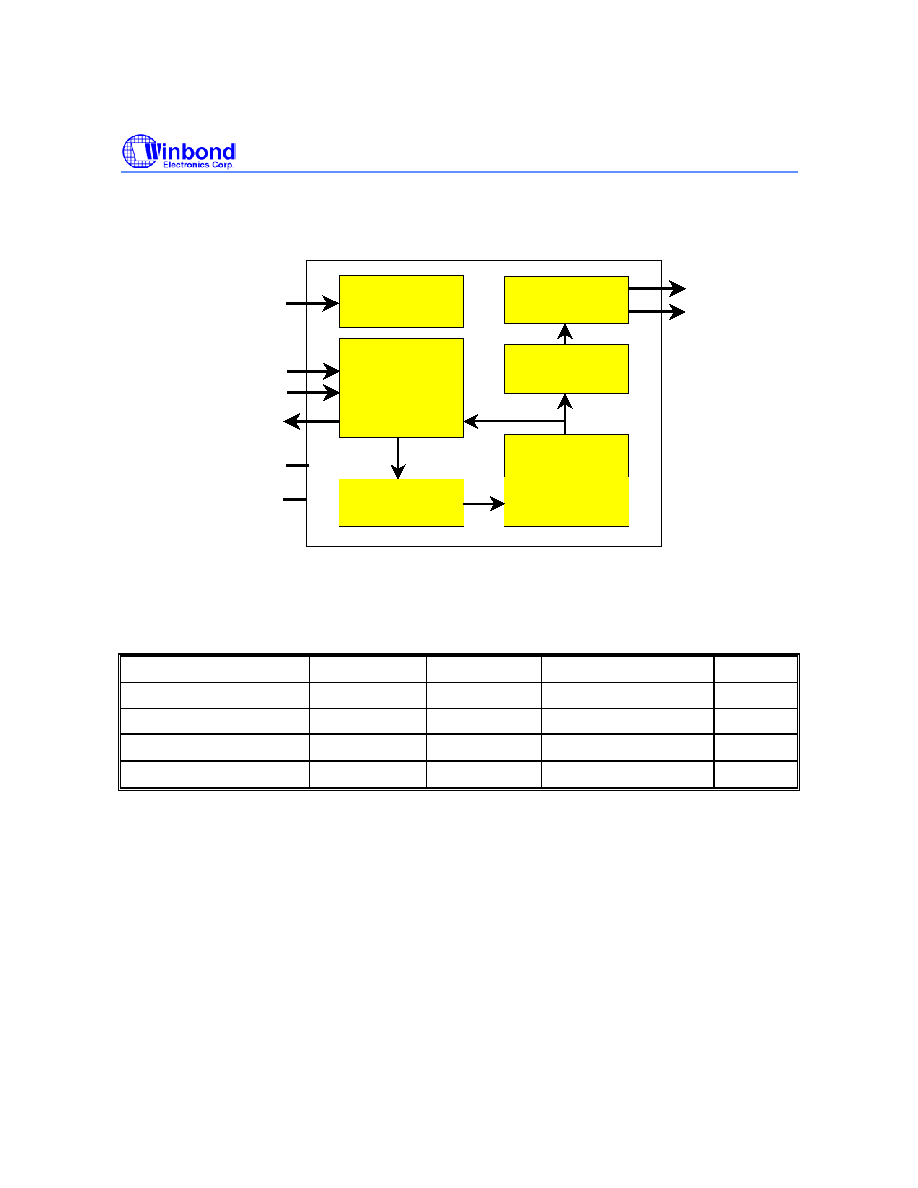
4. BLOCK DIAGRAM
O/P
V
SS
V
DD
TEST
OSC
CONTROL
LOGIC
PLA TABLE
PWM
COUNTER
ROM
TIMING
GENTRATOR
PWM+
PWM-
5. ABSOLUTE MAXIMUM RATINGS
PARAMETER SYMBOL
CONDITIONS
RATED
VALUE
UNIT
Power Supply
V
DD
-
V
SS
-
-0.3 to +7.0
V
Input Voltage
V
IN
All Inputs
V
SS
-0.3 to V
DD
+0.3 V
Storage Temp.
T
STG
-
-55 to +150
�C
Operating Temp.
T
OPR
-
0 to +70
�C
Note: Exposure to conditions beyond those listed under Absolute Maximum Ratings may adversely affect the life and reliability
of the device.
W522AXXX
Publication Release Date: June 3, 2003
- 5 -
Revision A2
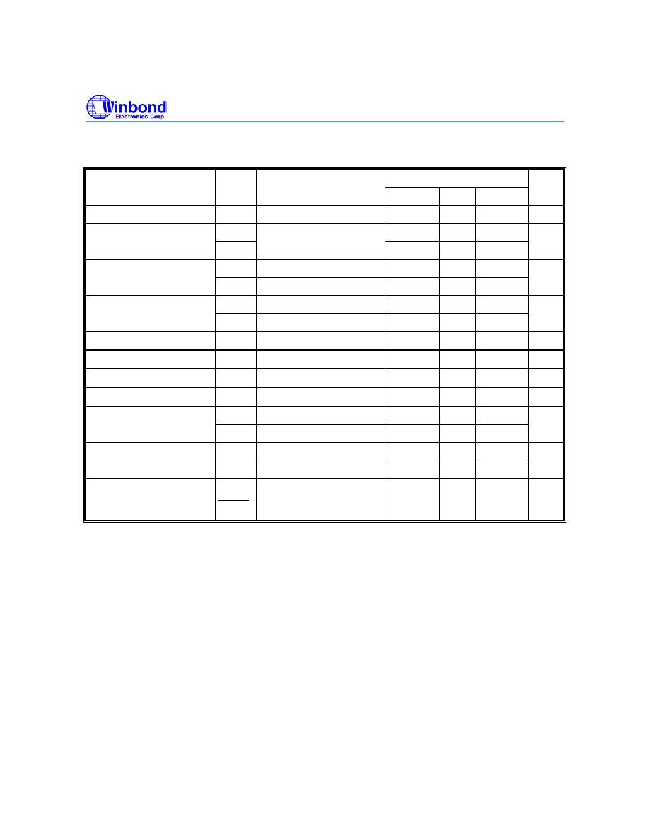
6. ELECTRICAL CHARACTERISTICS
(T
A
= 25
� C, V
SS
= 0 V)
LIMITS
PARAMETER
SYM.
CONDITIONS
MIN. TYP. MAX.
UNIT
Operating Voltage
V
DD
- 2.4
3
5.5
V
V
IL
V
SS
-0.3 - 0.3*V
DD
Input Voltage
V
IH
All Input Pins
0.7 V
DD
- V
DD
V
I
DD1
V
DD
= 3V, No Playing
-
-
1.0
Standby Current
I
DD2
V
DD
= 4.5V, No Playing
-
-
1.0
�A
I
OP1
V
DD
= 3V, No Load
-
-
4
Operating Current
I
OP2
V
DD
= 5V, No Load
-
-
8
mA
Input Current for TG
I
IN
V
DD
= 3V, V
IN
= 0V
4
8
12
�A
Input Current TEST
I
TEST
V
DD
= 3V, V
TEST
= 3V
6 10 20
�A
PWM Drive Current
I
PD
V
DD
= 3V, R
L
= 8
-130 - - mA
PWM Sink Current
I
PS
V
DD
= 3V, R
L
= 8
130 - - mA
I
OL
V
DD
= 3V, V
OUT
= 1V
10
-
-
Output Current
I
OH
V
DD
= 3V, V
OUT
= 2V
-5
-
-
mA
V
DD
= 3V, R
OSC
= Typ.
2.7
3
3.3
Oscillation Freq.
F
OSC
V
DD
= 4.5V, R
OSC
= Typ.
2.7 3 3.3
MHz
Oscillation Freq.
Deviation by Voltage
Drop
F
F
OSC
OSC
[F(5.5V)-F(2.4V)]/F(2.4V)
- - 10
%
Note: Rosc = typical value = 510K ohm

W522AXXX
- 6 -
7. APPLICATION CIRCUIT
W522AXXX
C
0.1 uF
Speaker 8 ohm
� watt
Rosc
O/P
V
DD
V
SS
PWM+
OSC
V
DD
PWM-
TG
R
100 ohm
Notes:
1. In principle, the playing speed determined by ROSC should correspond to the sampling rate during the coding phase.
The playing speed may be adjusted by varying ROSC. The typical value of Rosc is 510K ohm.
2. The capacitor, C (0.1uF), shunted between V
DD
and V
SS
is necessary for PWM output.
3. R is used to limit the current on the LED.
4. No warranty for production.

W522AXXX
Publication Release Date: June 3, 2003
- 7 -
Revision A2
8. REVISION HISTORY
REVISION DATE
MODIFICATIONS
A1
Jan- 2002
Preliminary release.
A2
June 3, 2003
Provides two part number W522A008, W522A010
Operation current max. 400 and 800uA 4 and 8 mA
Headquarters
No. 4, Creation Rd. III,
Science-Based Industrial Park,
Hsinchu, Taiwan
TEL: 886-3-5770066
FAX: 886-3-5665577
http://www.winbond.com.tw/
Taipei Office
TEL: 886-2-8177-7168
FAX: 886-2-8751-3579
Winbond Electronics Corporation America
2727 North First Street, San Jose,
CA 95134, U.S.A.
TEL: 1-408-9436666
FAX: 1-408-5441798
Winbond Electronics (H.K.) Ltd.
No. 378 Kwun Tong Rd.,
Kowloon, Hong Kong
FAX: 852-27552064
Unit 9-15, 22F, Millennium City,
TEL: 852-27513100
Please note that all data and specifications are subject to change without notice.
All the trade marks of products and companies mentioned in this data sheet belong to their respective owners.
Winbond Electronics (Shanghai) Ltd.
200336 China
FAX: 86-21-62365998
27F, 2299 Yan An W. Rd. Shanghai,
TEL: 86-21-62365999
Winbond Electronics Corporation Japan
Shinyokohama Kohoku-ku,
Yokohama, 222-0033
FAX: 81-45-4781800
7F Daini-ueno BLDG, 3-7-18
TEL: 81-45-4781881
9F, No.480, Rueiguang Rd.,
Neihu District, Taipei, 114,
Taiwan, R.O.C.