 | –≠–ª–µ–∫—Ç—Ä–æ–Ω–Ω—ã–π –∫–æ–º–ø–æ–Ω–µ–Ω—Ç: W5233 | –°–∫–∞—á–∞—Ç—å:  PDF PDF  ZIP ZIP |
Document Outline
- Main Menu
- Speech Products
- Search
- Web

W523X
Power Speech LOW VOLTAGE
ADPCM VOICE SYNTHESIZER
Publication Release Date: March 1996
- 1 -
Revision A2
GENERAL DESCRIPTION
The W523X is a programmable speech synthesis IC that utilizes the ADPCM coding method to
generate all types of voice effects. The W523X's LOAD and JUMP commands and four programmable
registers provide powerful user-programmable functions that make this chip suitable for an extremely
wide range of speech IC applications.
The W523X family includes the W5231, W5232, W5233, and W5234. The ROM size of each of these
products is shown below:
BODY
W5231
W5232
W5233
W5234
Second
3 Sec
6 Sec
9 Sec
12 Sec
Note: All of the playback lengths are estimated by typical applications.
FEATURES
∑
Wide operating voltage range: 1.2 to 3.6 volts
∑
Programmable speech synthesizer
∑
4-bit ADPCM synthesis method and 8-bit D/A converter
∑
RC oscillator with built-in capacitor; voice output frequency typically at 6 KHz
∑
Provides 4 trigger inputs
∑
Drives 2 flash LEDs for two batteries
∑
3 STOP output signals
∑
Flexible functions programmable through the following:
- LD (load), JP (jump) commands
- Four registers: R0, EN, STOP, and MODE
- Conditional instructions
- Speech equation
- Global repeat (GR) setting
∑
Programmable power-on initialization (POI), which can be interrupted by trigger inputs
∑
Interrupt or non-interrupt for rising or falling edge of each trigger pin (this feature determines
retriggerable, non-retriggerable, overwrite, and non-overwrite features of each trigger pin)
∑
LED On/Off control can be set independently in each GO instruction of speech equation
∑
Independent control of LED1 and LED2
∑
Total of 256 voice group entries available for programming
(including eight hardware and 248 software group entry points)
∑
20 to 40 mS debounce time
W523X
- 2 -
∑
Provides the following mask options:
- LED flash frequency: 3 Hz/6 Hz/Off
- LED flash type: synchronous/alternate
- LED1 section-controlled: Yes/No
- LED2 section-controlled/STPC-controlled
- AUD output current: 1 mA for one battery, 3 mA for two batteries
∑
Packaged in 20-pin DIP
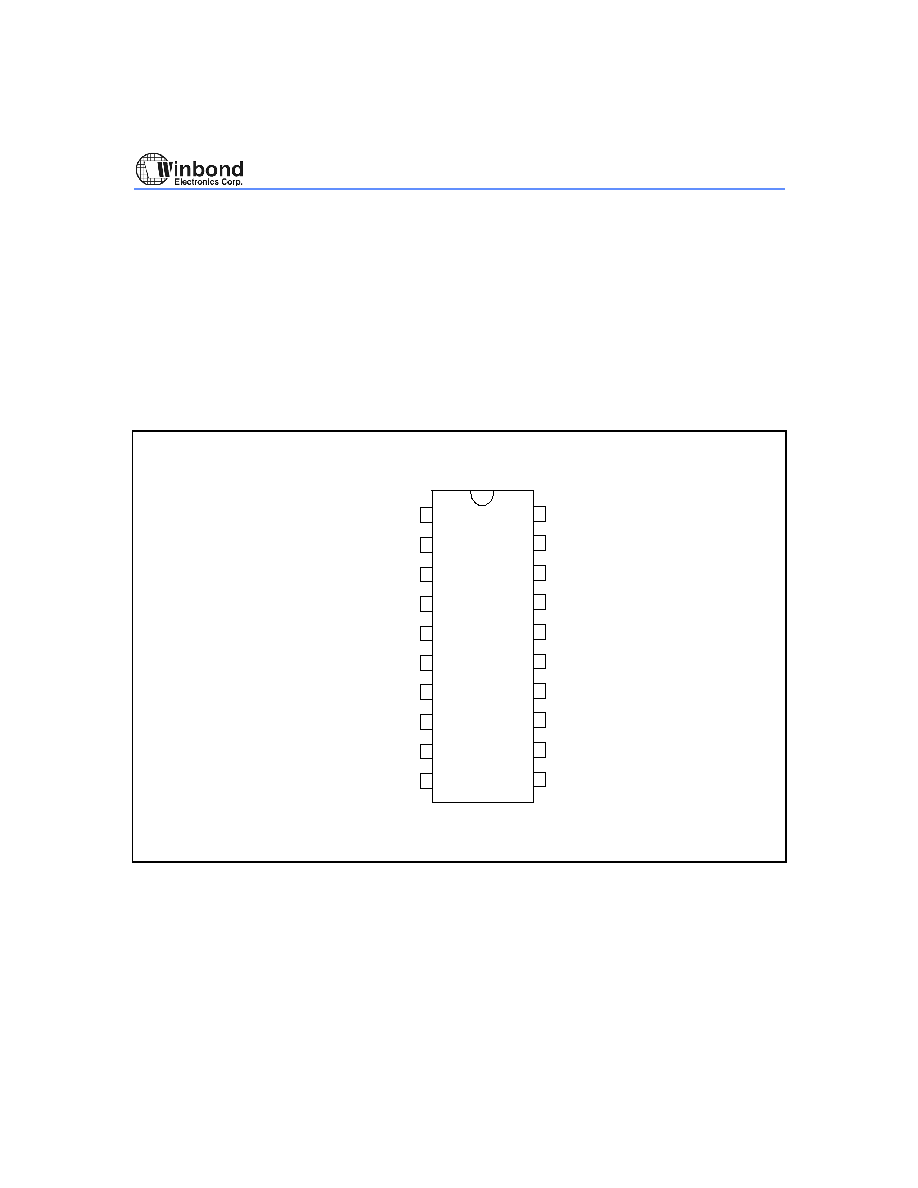
PIN CONFIGURATION
18
19
20
1
2
3
4
5
6
7
14
15
16
17
11
12
13
8
9
10
TG4/LED2/STPC
NC
NC
NC
V
TG1
TG2
TG3
LED1
STPB
STPA
NC
SPK
VSS
DD
TEST
NC
NC
NC
OSCO
OSCI

W523X
Publication Release Date: March 1996
- 3 -
Revision A2
PIN DESCRIPTION
PIN NO.
PIN NAME
I/O
FUNCTION
1
TG1
I
Trigger Input 1
2
TG2
I
Trigger Input 2
3
TG3
I
Trigger Input 3
4
TG4/LED2/STPC
I/O
Trigger Input 4 or LED 2 or Stop Signal C
5
LED1
O
LED 1
6
STPB
O
Stop Signal B
7
STPA
O
Stop Signal A
8
NC
-
Not Connected
9
SPK
O
Current Output for Speaker
10
V
SS
-
Negative Power Supply
11
V
DD
-
Positive Power Supply
12
OSCI
I
Oscillator Input Connect Resistor
13
OSCO
O
Oscillator Output Connect Resistor
14
NC
-
Not Connected
15
NC
-
Not Connected
16
NC
-
Not Connected
17
NC
-
Not Connected
18
NC
-
Not Connected
19
NC
-
Not Connected
20
TEST
I
Test Pin
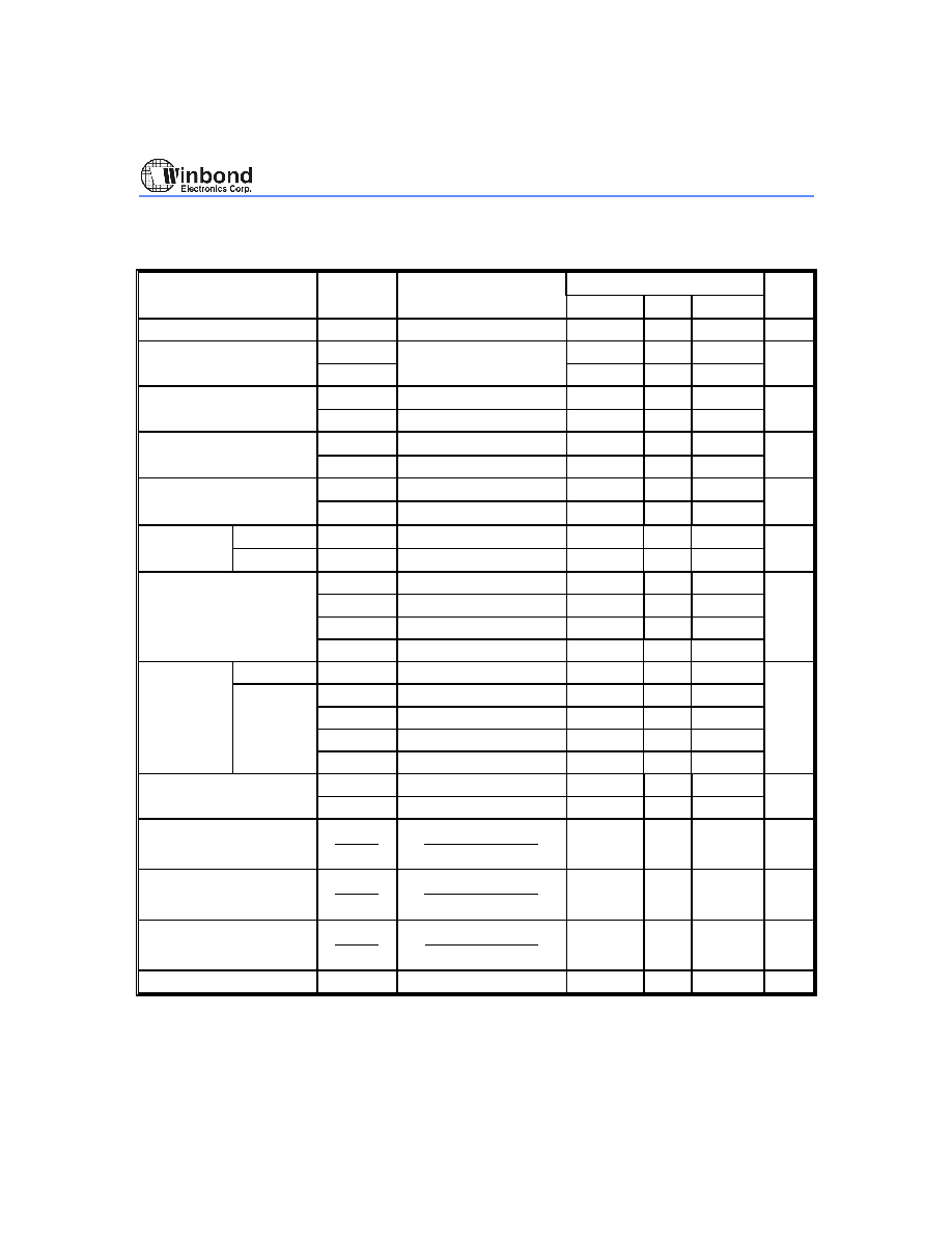
ABSOLUTE MAXIMUM RATINGS
PARAMETER
SYMBOL
CONDITIONS
RATED VALUE
UNIT
Power Supply
V
DD
-
V
SS
-0.3 to +5.0
V
Input Voltage
V
IN
All Inputs
V
SS
-0.3 to V
DD
+0.3
V
Storage Temp.
T
STG
-55 to +150
∞C
Operating Temp.
T
OPR
0 to +70
∞C
Note: Exposure to conditions beyond those listed under Absolute Maximum Ratings may adversely affect the life and reliability
of the device.
W523X
- 4 -
ELECTRICAL CHARACTERISTICS
(T
A
= 25
∞ C, V
SS
= 0 V)
PARAMETER
SYMBOL
CONDITIONS
LIMITS
UNIT
MIN.
TYP.
MAX.
Operating Voltage
V
DD
For One or Two Batteries
1.2
2.4
3.6
V
Input Voltage
V
IL
All Input Pins
V
SS
-0.3
-
0.3 V
DD
V
V
IH
0.7 V
DD
-
V
DD
Standby Current
I
DD1
V
DD
= 3 V, No Playing
-
-
0.5
µA
I
DD2
V
DD
= 1.5 V, No Playing
-
-
0.3
Operating Current
I
OP1
V
DD
= 3 V, No Load
-
-
400
µA
I
OP2
V
DD
= 1.5 V, No Load
-
-
250
Input Current For
I
lN1
V
DD
= 3 V, V
IN
= 0 V
-
-
5
µA
TG1
-TG4
I
IN2
V
DD
= 1.5 V, V
IN
= 0 V
-
-
2.5
SPK (D/A
Option1
I
O1
V
DD
= 1.5 V, R
L
= 200
-0.8
-1.0
-1.2
mA
Full scale)
Option2
I
O2
V
DD
= 3 V, R
L
= 200
-2.0
-3.0
-4.0
l
OL1
V
DD
= 3V, V
OUT
= 0.4V
1
-
-
mA
Output Current of
I
OL2
V
DD
= 1.5V, V
OUT
= 0.4V
1
-
-
SPTC
I
OH1
V
DD
= 3 V, V
OUT
= 2.7 V
-0.5
-
-
l
OH2
V
DD
= 1.5 V, V
OUT
= 1.2 V
-0.3
-
-
LED
I
O
V
DD
= 3 V, V
OUT
= 1 V
6
-
-
mA
Output
I
OL1
V
DD
= 3 V, V
OUT
= 0.4 V
1
3
-
Current
STPA
l
OL2
V
DD
= 1.5 V, V
OUT
= 0.4 V
1
2
-
STPB
l
OH1
V
DD
= 3 V, V
OUT
= 2.7 V
-1
-3
-
I
OH2
V
DD
= 1.5 V, V
OUT
= 1.2 V
-0.3
-
-
Oscillation Freq.
F
OSC1
V
DD
= 3 V, R
OSC
= Typ.
320
384
460
KHz
F
OSC2
V
DD
= 1.5 V, R
OSC
= Typ.
320
384
460
Oscillation Freq. Deviation
by Voltage Drop
F
F
OSC
OSC
F(1.5 V)
F(1.2 V)
F(1.5 V)
-
0
10
20
%
Oscillation Freq. Deviation
by Voltage Drop
F
F
OSC
OSC
F(1.8 V)
F(1.5 V)
F(1.8 V)
-
0
4
7.5
%
Oscillation Freq. Deviation
by Voltage Drop
F
F
OSC
OSC
F(3.0 V)
F(2.4 V)
F(3.0 V)
-
0
4
7.5
%
Input Debounce Time
T
DEB
F
OSC
= 384 KHz
20
30
40
mS
Note: R
OSC
= Typ.= 100 K
for one battery; 110 K for two batteries.

W523X
Publication Release Date: March 1996
- 5 -
Revision A2
TYPICAL APPLICATION CIRCUIT
DD
18
19
20
NC
NC
NC
TEST
1
2
3
4
5
6
7
8
13
14
15
16
17
NC
NC
NC
11
12
Rosc
9
10
TG1
TG2
TG3
TG4/LED2/STPC
LED1
STPB
STPA
NC
SPK
R
Cs
8050D
V
V
V
W523X
OSCO
OSCI
R
s
DD
SS
Speaker
8 ohm
1/4 watt
Notes:
1. In principle, the playing speed determined by R
OSC
should correspond to the sampling rate during the coding phase.
The playing speed may be adjusted by varying R
OSC
, however.
2. Rs is an optional current-dividing resistor. If Rs is added, the resistance should be between 470 and 750
.
3. R is used to limit the current on the LED.
4. Cs is optional.
5. The DC current gain
of transistor 8050 ranges from 120 to 200.
6. All unused trigger pins can be left open because of their internal pull-high resistance.
7. No warranty for production!

W523X
- 6 -
Headquarters
No. 4, Creation Rd. III,
Science-Based Industrial Park,
Hsinchu, Taiwan
TEL: 886-3-5770066
FAX: 886-3-5792697
http://www.winbond.com.tw/
Voice & Fax-on-demand: 886-2-7197006
Taipei Office
11F, No. 115, Sec. 3, Min-Sheng East Rd.,
Taipei, Taiwan
TEL: 886-2-7190505
FAX: 886-2-7197502
Winbond Electronics (H.K.) Ltd.
Rm. 803, World Trade Square, Tower II,
123 Hoi Bun Rd., Kwun Tong,
Kowloon, Hong Kong
TEL: 852-27516023
FAX: 852-27552064
Winbond Electronics North America Corp.
Winbond Memory Lab.
Winbond Microelectronics Corp.
Winbond Systems Lab.
2730 Orchard Parkway, San Jose,
CA 95134, U.S.A.
TEL: 1-408-9436666
FAX: 1-408-9436668
Note: All data and specifications are subject to change without notice.