�
�
�
�
Publication Release Date: Sep 2000
- 1 - Revision A7
GENERAL DESCRIPTION
The W536XXXA, a member of ViewTalk
TM
family, is a high-performance 4-bit micro-controller (uC) with
built-in speech unit, melody unit and 64seg * 16 com LCD driver unit which includes internal regulator
,pump circuit and dedicated two pages LCD RAM. The 4-bit uC core contains dual clock source, 4-bit
ALU, two 8-bit timers, one 14 bits divider, maximum 24 pads for input or output, 8 interrupt sources and
8-level nesting for subroutine/interrupt applications. Speech unit, integrated as a single chip with
maximum 128 seconds (based on 6.4K sample rate with 5 bits MDPCM) , is capable of expanding to
512 seconds speech addressed by external memory W55XXX with serial bus interface. It can be
implemented with Winbond Power Speech using MDPCM algorithm. Melody unit provides dual tone
output and can store up to 1k notes. Power reduction mode is also built in to minimize power dissipation.
It is ideal for games, educational toys, remote controllers, watches, clocks and other application
products which incorporate both LCD display and speech.
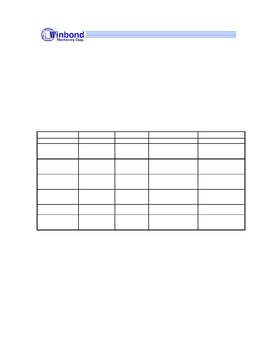
Body W536030A
W536060A
W536090A
W536120A
Voice
30 sec
60 sec
90 sec
120 sec
I/O pad
4I/O,8I
(RA/RC/RD)
8I/O, 8I
(RA/RB/RC/RD)
8I/O, 8I , 8O
(RA/RB/RC/RD/RE/RF)
8I/O, 8I, 8O
(RA/RB/RC/RD/RE/RF
)
WDT
disable/Enable
(Mask Option)
Y Y
Y
Y
Sub-clock
RC/XTAL mode
(Mask Option)
Y Y
Y
Y
RD port shared as
serial bus
(Mask Option)
Y(1) Y(1)
N
N
(2)
Tri-state serial bus
(Mask Option) ( 3)
Y Y
N
N
Cascaded Voice
ROM through
serial bus (2)
Y(1) Y(1)
N
Y
(1) Share 3 pads of RD port (RD1/RDP, RD2/SPDATA and RD3/WRP)
(2) Dedicate serial bus 3 pads (RDP, SPDATA and WRP) to interface with W55XXX. Cascaded
Voice ROM can help to expand voice up to 512 sec by W55XXX chip.
(3) Tri-state serial bus mask option can float serial bus while voice playing is no active. Let this
mask option is disabled to get minimum power consumption in general.
FEATURES
�
Operating voltage: 2.4 volt ~ 5.5 volt
�
Watch dog disabled/enabled by mask option
�
Dual clock operating system
-
Main clock with RC/Crystal (400 KHz to 4 MHz)
-
Sub-clock with 32.768 KHz RC/Crystal by mask option

Publication Release Date:Sep 2000
- 2 - Revision A7
�
Memory
-
Program ROM (P-ROM): 32K
�
20 (ROM Bank0, 1, 2)
-
Data RAM (W-RAM): 1.4K
�
4 bit
(RAM Bank 0 is 896 nibbles from 0:000 ~0:37F and 0:380~0:3FF are mapped to special register.
RAM Bank F is 512 nibbles from F:200 ~F:3FF either data RAM or dedicated to script kernel )
-
LCD RAM (L-RAM): 256
�
4 bit
�
2 pages (RAM Bank1, 2 from 200~2FF)
�
Maximum 24 input/output pads
-
Ports for input only: 8 pads (RC, RD port; RD1~3 can share as serial bus for external memory
W55XXX interface @W536030A/060A)
-
Ports for output only: 8 pads (RE & RF port; W536090A/120A available only)
-
Ports for Input/output: 8 pads (RA and RB port; RB port is available for W536060A/090A/120A
only)
�
Power-down mode
-
Hold mode (except for 32kHz oscillator)
-
Stop mode (including 32kHz oscillator and release by RD or RC port)
�
Eight types of interrupts
-
Five internal interrupts (Divider, Timer 0, Timer 1, Speech, Melody)
-
Three external interrupts (Port RC, RD, RA)
�
One built-in 14-bit clock frequency divider circuit
�
Two built-in 8-bit programmable countdown timers
-
Timer 0: one of two clock sources (FOSC/4 or FOSC/1024) can be selected
-
Timer 1: built-in auto-reload function includes internal timer, external event counter from RC.0
�
Built-in 18/14-bit watchdog timer for system reset.
�
Powerful instruction sets
�
8-level subroutine (including interrupt) nesting
�
LCD driver unit capability
-
VLCD higher than (VDD-0.5V)
-
Built-in voltage regulator to V2 pad
-
64 seg
�
16 com
-
1/16 or 1/8 duty, 1/5 or 1/4 bias, internal pump circuit option by special register
-
COM 8~ 15 and SEG40~63 can be shared as general input/output by special register
-
Either uC ROM or voice ROM used as LCD picture
�
Speech function
-
Provided 1M / 2M/ 3M/ 4M bits Voice ROM for W536030A/060A/090A/120A based on 5 bits
MDPCM algorithm
-
Voice ROM (V-ROM) available for uC data or LCD picture data.
-
Maximum 8*256 Label/Interrupt vector (voice section number) available
-
Provide two types of speech busy flag to either each GO or each trigger
-
Maximum up to 16M bits speech address capability interface with external memory W55XXX
through serial bus.
�
Melody function
-
Provide 1K notes (22bits/note) dedicated melody ROM
-
Provide two types of melody busy flag to uC either each note or each song
-
Provide 6 kinds of beat, 16 kinds of tempo, and pitch range from G3# to C7
-
Tremolo, triple frequency and 3 kinds of percussion available
-
Maximum 31 songs available
�
Can mix speech with melody
�
Multi-engine controller
�
Direct driving speaker/buzzer or DAC output
�
Chip On Board available

Publication Release Date:Sep 2000
- 3 - Revision A7
BLOCK DIAGRAM
XIN XOUT X32I X32O
LCD DRIVER
PC
STACK
(8 Levels)
Timer 0
Timing
Generator
SEG0~63
V3,V4,V5,V6
Timer 1
Watch Dog
ALU
ACC
Divide
ROM
32K*20Bit
DH1,DH2
COM0~15
RAM
1.4*4Bit
Special Register
HCF
HEF
IEF
EVF
FLAG1
PSR0
MR0
PEF
FLAG0
LPX3
PM0
LPX2
LPX0
LPX1
PORT RA
VLCD PUMP &
REGULATOR
TONE
RA0~3
RES
LPX4
PORT RC
PORT RD
RC0~3
RD0~3
LPX5 LPY0
LPY1
SPC
MLD
Dual
Tone
melody
(1K notes)
MLD_play
MLD_busy
Speech
MDPCM
core
SPC_play
SPC_busy
PWM1/DAC
ROSC
Parallel
to Serial
Interrupt ,Hold & Stop
Control
RE0~3
RF0~3
PORT RB
RB0~3
PORT RE
PORT RF
WRP
RDP
SPDATA
V2
VDD
VSS
VSSP
TEST
Voice ROM
(1M /2M/3M/4M bits)
PWM/DAC
Mix
Block
PWM2
VDDP
LPXY
Shared_ROM Data

Publication Release Date:Sep 2000
- 4 - Revision A7
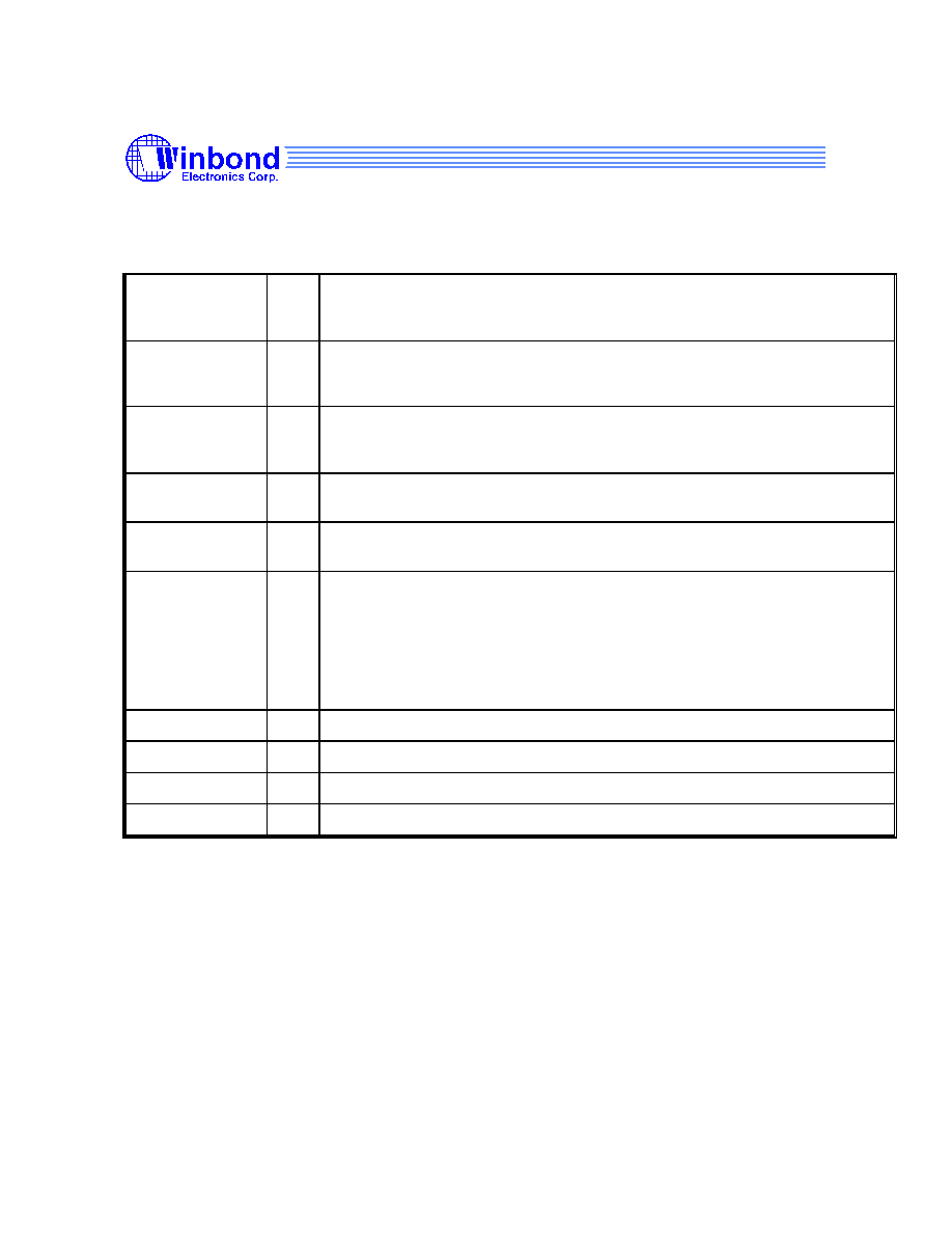
PAD DESCRIPTION
SYMBOL I/O
FUNCTION
XIN/RXIN
I
Input pad for main clock oscillator. It can be connected to crystal when crystal
mode is selected (SCR0.2=1), otherwise connect a resistor to VDD to generate
main system clock while RC mode is selected (SCR0.2=0 and default). Oscillator
can be enabled or stopped by set SCR0.1 to 1 or clear to 0 separately. External
capacitor connects to start oscillation while crystal mode
XOUT
O
Output pad for oscillator which is connected to another crystal pad when in crystal
mode. External capacitor connects to start oscillation when in crystal mode.
X32I/RSUB1 I 32.768 KHz crystal input pad or external resistor node 1 by mask option.
External 15~20pF capacitor connects to get more accurate clock when in crystal
mode.
X32O/RSUB2 O 32.768 KHz crystal output pad or external resistor node 2 by mask option.
External 15~20pF capacitor connects to get more accurate clock when in crystal
mode.
RA0 ~ RA3/TONE I/O
General Input/Output port specified by PM1 register. If output mode is selected,
PM0 register bit 0 can be used to specify CMOS/NMOS driving capability option.
Initial state is input mode. RA3 may be uses as TONE if bit 0 of MR0 special
register is set to logic 1. An interrupt source.
RB0 ~ RB3
I/O
General Input/Output port specified by PM2 register. If output mode is selected,
PM0 register bit 1 can be used to specify CMOS/NMOS driving capability option.
Initial state is input mode (W536060A/090A/120A only.)
RC0 ~ RC3
I 4-bit
sch
mitter input with internal pull high option specified by PM3 register bit 2. Each pad
has an independent interrupt capability specified by PEFL special register.
Interrupt and STOP mode wake up source. RC0 is also the external event
counter source of Timer1.
RD0
RD1/RDP
RD2/SPDATA
RD3/WRP
(4)
I
4-bit schmitter input port with internal pull high option specified by PM3 register
bit 3. Each pad has an independent interrupt capability specified by PEFH
special register. Interrupt and STOP mode wake up source. RD1~3 will be
shared as the external memory W55XXX interface pads while RD port shared as
serial bus mask option is enabled @W536030A/060A.
For W536030A/060A only, "Tri-state serial bus" mask option can use to float
WRP/RDP/SPDATD while "RD port shared as serial bus" mask option is
enabled.
RE0~RE3
O Output port only. PM3 register bit 0 can be used to specify CMOS/NMOS driving
capability option. (W536090A/120A only)
RF0~RF3
O
Output port only. PM3 register bit 1 can be used to specify CMOS/NMOS driving
capability option. (W536090A/120A only)
RES
I
System reset pad, active low with internal pull-high resistor.

Publication Release Date:Sep 2000
- 5 - Revision A7
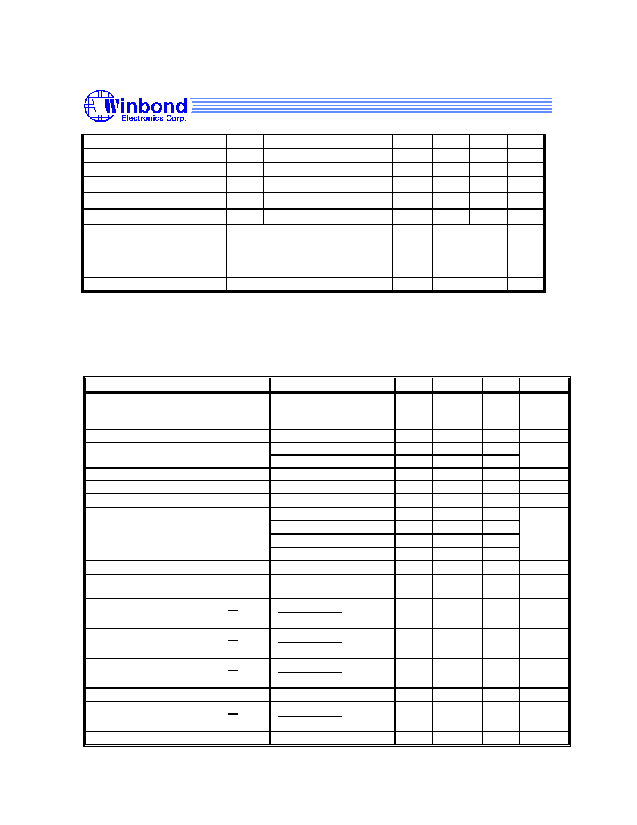
TEST
I
Test pad. Active high with internal pull low resistor.
ROSC
I
Connect resistor to VDD pad to generate speech or melody playing clock source.
PWM1/DAC
O
While speech or melody is active , PWM1/DAC is speaker direct driving output
or DAC output controlled by voice output file.
PWM2
O
While speech or melody is active, PWM2 is another speaker direct driving output.
WRP (5)
O
External serial memory address write clock for voice extension (W536120A only).
RDP (5)
O
External serial memory address read clock for voice extension. (W536120A only).
SPDATA (5)
I/O
External serial memory data in/out for voice extension (W536120A only).
SEG0
-
SEG39
O
Dedicated LCD segment output pads.
SEG40/PORTN.0
SEG43/PORTN.3
O/O
LCD segment output pads, and can be shared as general output by register
LCDM3 bit 1. Default function is segment pad.
SEG44/PORTM.0
SEG47/PORTM.3
O/I
LCD segment output pads, and can be shared as general input by register
LCDM3 bit 0. Default function is segment pad and PM5.1=0 to inhibit LCD
waveform abnormal.
SEG48/PORTL.0
SEG51/PORTL.3
O/O
LCD segment output pads, and can be shared as general output by register
LCDM2 bit 0. Default function is segment pad.
SEG52/PORTK.0
SEG55/PORTK.3
O/I
LCD segment output pads, and can be shared as general input by register
LCDM2 bit 1. Default function is segment pad and PM5.0=0 to inhibit LCD
waveform abnormal.
SEG56/PORTJ.0
SEG59/PORTJ.3
O/IO LCD segment output pads, and can be shared as general input/output by register
LCDM2 bit 2. PM4 register is used to select input or output while shared I/O
function is active. Default function is segment pad and PM4.3=0 to inhibit LCD
waveform abnormal.
SEG60/PORTI.0
SEG63/PORTI.3
O/IO LCD segment output pads, and can be shared as general input/output by register
LCDM2 bit 3. PM4 register is used to select input or output while shared I/O
function is active. Default function is segment pad and PM4.2=0 to inhibit LCD
waveform abnormal.
Publication Release Date:Sep 2000
- 6 - Revision A7
COM0
-
COM7
O
LCD common signal output pads either 1/16 duty or 1/8 duty. The LCD frame rate
is controlled by LCDM1 register, and default value LCDM1=0111b with 64Hz
frame rate.
COM8 / PORTP.0
COM11/PORTP.3
O/O
LCD common signal output pads, or shared as general output by register
LCDM3.2 when in 1/8 duty mode. Default function is common function.
COM12/PORTO.0
COM15/PORTO.3
O/I
LCD common signal output pads, or shared as general input by register LCDM3.2
when in 1/8 duty mode. Default function is common function and PM5.2=0 to
inhibit LCD waveform abnormal.
DH1, DH2 (6)
O
Connection terminal for voltage double capacitor with 0.1uF. The DH2 connects
to capacitor positive node and DH1 negative node if polar capacitor is used.
V3 ~ V6 (6)
O
LCD COM/SEG output driving voltage. Need an external 0.1uF capacitor to every
pad terminal.
V2 (6)
I/O
Voltage regulator output pad. An external capacitor is a must. Output level can
be controlled from 0~Fh by LCDM4 register. If internal pump is enabled
(LCDM3.3=0 and default value), LCD operating voltage (VLCD) will be 4*V2 or
5*V2 depending on 1/4 bias or 1/5 bias. A limitation should be noted that VLCD
must be higher than (VDD-0.5v) to avoid chip leakage current. While external
reference voltage is selected (LCDM3.3=1), V2 pad input voltage can not be over
1.5 Volt to inhibit chip damage
.
VSSP (7)
I
Power ground for PWM or DAC playing output.
VSS (7)
I
Power ground
VDDP (7)
I
Power source for PWM or DAC playing output.
VDD (7)
I
Power source.
(4) RD1~3 are shared as RDP/SPDATA/WRP to interface with W55XXX @W536030A/060A
(5)
@W536120A only
(6) 0.1uF is default value, and capacitor value should be larger than 0.1uF if LCD dot size over
0.5mm * 0.5mm.
(7)
External application circuit should connect together, please refer to APPLICATION CIRCUIT. To
sure chip operation properly, please bond all VDD, VDDP,VSS and VSSP pads and connect VSS
and VSSP from chip outside PCB circuit.

Publication Release Date:Sep 2000
- 7 - Revision A7
ABSOLUTE MAXIMUM RATINGS
PARAMETER RATING
UNIT
Supply Voltage to Ground Potential
-0.3 to +7.0
V
Applied Input/Output Voltage
-0.3 to +7.0
V
Power Dissipation
120
mW
Ambient Operating Temperature
0 to +70
�
C
Storage Temperature
-55 to +150
�
C
Note: Exposure to conditions beyond those listed under Absolute Maximum Ratings may adversely affect
the life and reliability of the device.
DC CHARACTERISTICS
(VDD
-
VSS = 3.0V, No load, F
M
= 4 MHz with RC mode, Fs = 32.768 KHz, with Xtal mode, T
A
= 25
�
C,
STN LCD panel on with dot size 0.5mm*0.5mm; unless otherwise specified)
PARAMETER
SYM. CONDITIONS
MIN
TYP
MAX
UNIT
Op. Voltage
V
DD
2.4
5.5
V
Op. Current
I
OP1
Dual clock with crystal
-
600
700
uA
(No Load, no Voice, no )
Dual clock with RC type
600
700
Melody)
Sub-clock only, LCD off
40
50
Sub-clock only, LCD on
70
90
Hold Mode Current
(No Load, LCD OFF)
I
OP2
Sub-clock active only
6
10
uA
Hold Mode Current
(No load, LCD ON)
I
OP3
Sub-clock active only
70
uA
Stop Mode Current
I
OP4
LCD auto off
1
uA
RDP/WRP Output High
Current
Io
H1
Vout=2.7V
-0.8
mA
RDP/WRP Output low
Current
Io
L1
Vout=0.4V
0.8 mA
Input Low Voltage
V
IL
- VSS
-
0.3
VDD
Input High Voltage
V
IH
-
0.7
-
1
VDD
Port RA, RB Output Low
Voltage
V
ABL
IOL = 2.0 mA
-
-
0.4
V
Port RA, RB Output High
Voltage
V
ABH
IOH = -2.0 mA
2.4
-
-
V
Pull-up Resistor
R
CD
Port RC, RD
200
300
400
K
RES Pull-up Resistor
R
RES
- 50
100
200
K
PWM1/2 Source Current (8)
I
SPH
Volume Option =00
-20
mA
(R
LOAD
=8
between PWM1
Volume Option =01
-70
And PWM2 )
Volume Option =10
-110
Volume Option =11
-135
PWM1/2 Sink Current (8)
I
SPL
Volume Option =00
20
mA
(R
LOAD
=8
between PWM1
Volume Option =01
70
And PWM2 )
Volume Option =10
110
Volume Option =11
135
Publication Release Date:Sep 2000
- 8 - Revision A7
DAC output Current
I
DAC
VDD=3v,
RL=100ohm -4 -5 -6 mA
LCD Supply Current
I
LCD
No Load, All Seg. ON
-
50
-
�
A
COM/SEG On Resistor
R
ON
IOH =
�
50
�
A
5K
10K
V2 Pad Output Voltage
V
RR
Depended on LCDM4
0.7
1.45
V
V2 Pad Output Deviation (9) V
D1
No Load
�
5
%
V2 Pad Voltage Step
V
R2
LCDM4 increased 1
50
mV
V6 Pad Output Voltage
(LCD's VLCD depended on
V
LCD
1/4 Bias & no load
3.8
* V2
3.85
* V2
3.9
* V2
V
LCDM4 register) (9)
1/5 Bias & no load
4.75
* V2
4.8
* V2
4.85
* V2
V2 input voltage
V
EXT
LCDM3.3=1
1.5
V
(8)
PWM current deviation will be
�
20%.
(9)
Deviation is governed by LCD dot size. More larger LCD dot will get larger deviation..
AC CHARATERISTICS
(VDD
-
VSS = 3.0V, No load, F
M
= 4 MHz with RC mode, Fs = 32.768 KHz, with Xtal mode, T
A
= 25
�
C,
STN LCD on with dot size 0.5mm*0.5mm; unless otherwise specified)
PARAMETER
SYM.
CONDITIONS
MIN.
TYP.
MAX. UNIT
Sub-clock Frequency
F
SUB
Crystal type and X32IN
and X32O with 17pF
external cap.
32768
Hz
Main-clock Frequency
F
M
RC type/Crystal type
400K -
4M
Hz
Chip Operation Frequency
F
OSC
SCR0.0=1,F
SYS
=F
SUB
32768
Hz
SCR0.0=0;F
SYS
= F
MAIN
400K
-
4M
Instruction Cycle Time
T
CYC
One machine cycle
-
4/F
OSC
- S
Reset Active Width
T
RAW
FOSC = 32.768 KHz
1
-
-
�
S
Interrupt Active Width
T
IAW
FOSC = 32.768 KHz
1
-
-
�
S
Main clock RC frequency
F
RXIN
RXIN =680K
1M Hz
(10)
RXIN =330K
2M
RXIN =200K
3M
RXIN =130K
4M
Sub-Clock Ring Oscillator
F
RSUB
R
SUB
=680K
32 KHz
Sub-Clock Oscillation
Stable Time @ Cold Start
F
STOP
R
SUB
=680K
0.8
1 S
Frequency Deviation of
main-clock F
RXIN
2MHz
f
f
f(3V) f(2.4V)
f(3V)
-
10
%
Frequency Deviation of
main-clock F
RXIN
= 3 MHz
f
f
f(3V) f(2.4V)
f(3V)
-
15
%
Frequency Deviation of
main-clock F
RXIN
=4 MHz
f
f
f(3V) f(2.4V)
f(3V)
-
20
%
ROSC Frequency
F
ROSC
R
OSC
=680K
3
MHz
Frequency Deviation of
F
ROSC
= 3MHz
f
f
f(3V) f(2.4V)
f(3V)
-
7.5
%
Frame frequency
F
LCD
LCDM1=0111 b(default)
64
Hz
(10)
The deviation will be +20% while VDD drops from 5.5V to 2.4V based on same resistor

Publication Release Date:Sep 2000
- 9 - Revision A7
Iop Vs. Main clock RC mode
0
200
400
600
800
1000
1
2
3
4
Freq (MhZ)
Iop (uA)
3V
4.5V
Oscillation Freq Vs. Sub-Clock
20
24
28
32
36
40
44
560
620
680
750
820
1K
Rsub (Kohm)
Fsub (KhZ)
3V
4.5V

Publication Release Date:Sep 2000
- 10 - Revision A7
Main Freq Vs. Rxin
0
1
2
3
4
5
6
130 150 160 200 330 680 2K
3K
RXIN (Kohm)
Fmain
(MhZ)
2.4V
3v
4.5V
5.5V
Voice Operating Freq. Vs. ROSC
2
2.5
3
3.5
4
4.5
470
560
680
910
ROSC (Kohm)
Freq (MhZ)
3V
4.5V

Publication Release Date:Sep 2000
- 11 - Revision A7
APPLICATION CIRCUIT--1: Sub clock with RC mode
VLCD> (VDD-0.5v)
Panel
W536xxxA
RC0~3
RD0~3
RA0~3
RB0~3
RE0~3
X32IN
X32O
Battery
R4
C10
VDDP
R1
R3
ROSC
XIN
RES
C9
VDDP
COM0~15
SEG0~63
PWMN
PWMP/DAC
RF0~3
(
*
2)
R5
C4
V4
C6
V6
C5
V5
C2
V2
C3
V3
C1
DH2
DH1
470
(*3)
(*1)
VDD
C11
R2
VSSP
VSS
VDD
+
-
Component
C1~C6
C7,C8
C9,C10
C11
R1 R2 R3
R4
Value 0.1uF
- 0.1uF
1uF
680K
680K
680Kohm/1Mhz
330Kohm/2Mhz
200Kohm/3Mhz
130Kohm/4Mhz
100
Note:
(1) C1~C6 depends on LCD panel dot size.
(2) Option R5 equals to 100
if high noise immunity is needed.
(3) For DAC option application.
(4)
To sure chip operation properly, please bond all VDDP, VDD, VSSP and VSS .

Publication Release Date:Sep 2000
- 12 - Revision A7
APPLICATION CIRCUIT---2 : Sub clock with Crystal mode
VLCD> (VDD-0.5v)
Panel
W536xxxA
RC0~3
RD0~3
RA0~3
RB0~3
RE0~3
Battery
R4
C10
VDDP
R1
R3
ROSC
XIN
RES
C9
VDDP
COM0~15
SEG0~63
PWMN
PWMP/DAC
RF0~3
(
*
2)
R5
C4
V4
C6
V6
C5
V5
C2
V2
C3
V3
C1
DH2
DH1
470
(*3)
(*1)
VDD
C11
VSSP
VSS
VDD
32.768kHz
C7
X32IN
X32O
C8
+
-
Component
C1~C6
C7,C8 C9,C10
C11
R1 R2
R3
R4
Value 0.1uF
15~20pF
0.1uF
1uF
680K
-
680Kohm/1Mhz
330Kohm/2Mhz
200Kohm/3Mhz
130Kohm/4Mhz
100
Note:
(1) C1~C6 depends on LCD panel dot size.
(2) Option R5 equals to 100
if high noise immunity is needed.
(3) For DAC option application.
(4)
To sure chip operation properly, please bond all VDDP, VDD, VSSP and VSS .