 | –≠–ª–µ–∫—Ç—Ä–æ–Ω–Ω—ã–π –∫–æ–º–ø–æ–Ω–µ–Ω—Ç: W682510 | –°–∫–∞—á–∞—Ç—å:  PDF PDF  ZIP ZIP |

ADVANCED
W682510/W682310
DUAL-CHANNEL VOICEBAND CODECS
Publication Release Date: May 2003
- 1 -
Revision 0.35

W682510/W682310
1. GENERAL DESCRIPTION
The W682510 and W682310 are general-purpose dual channel PCM CODECs with pin-selectable
µ
-
Law or A-Law companding. The device is compliant with the ITU G.712 specification. It operates from
a single power supply (+5V for the W682510, +3V for the W682310) and is available in 20-pin PDIP
(W682510 only), SSOP, and 24-pin SOP package options. Functions performed include digitization
and reconstruction of voice signals, and band limiting and smoothing filters required for PCM systems.
The filters are compliant with ITU G.712 specification. The W682510 and W682310 performance is
specified over the industrial temperature range of ≠40
∞
C to +85
∞
C.
The W682510 includes an on-chip precision voltage reference and receive output buffer amplifiers,
capable of driving 600
loads (line transformers.) The analog section is fully differential, reducing
noise and improving the power supply rejection ratio. The data transfer protocol supports either
parallel or serial synchronous communications for PCM applications. The W682510 and W682310
have a build in PLL that eliminates the need for a master clock and automatically determines the
division ratio for the required internal clock.
For fast evaluation and prototyping purposes, the W682510DK & W682310DK development kits are
available.
2. FEATURES
∑
Single power supply
o
4.5V to 5.5V (W682510)
o
2.7V to 3.8V (W682310)
∑
Typical power dissipation of 35 mW,
power-down mode of 5
µ
W
∑
Fully-differential analog circuit design
∑
On-chip precision reference-
o
W682510: 1.73V for a 0.8 dBm
0TLP at 600
o
W682310: 1.41V reference for a
0TLP of ≠3.8 dBm into 1200
∑
Pin-selectable
µ
-Law and A-Law
companding (compliant with ITU G.711)
∑
CODEC A/D and D/A filtering compliant
with ITU G.712
∑
Industrial temperature range (≠40
∞
C to
+85
∞
C)
∑
Three packages: 20-pin SSOP, 20-pin
PDIP, and 24-pin SOP
APPLICATIONS
∑
Digital Telephone Systems
∑
Central Office Equipment (Gateways,
Switches, Routers)
∑
PBX Systems (Gateways, Switches)
∑
PABX/SOHO Systems
∑
Hands free system
∑
Speakerphone devices
∑
VoIP Terminals
∑
Enterprise Phones
∑
ISDN Terminals
∑
Analog line cards
- 2 -

W682510/W682310
3. BLOCK DIAGRAM
PLL
µ
/A
-
Law
CODEC
Filter 1
µ
/A
-
Law
CODEC
Filter 2
V
SSA
V
SSD
PU
I
V
DD
Power Conditioning
RO1
AO1
-
AI1
Voltage reference
V
REF
RO2
AO2
-
AI2
µ
/A
-
Law
BCLK
PC
M
Int
erf
ac
FSR
FST
PCMT2
PCMT1
PCMR1
PCMR2
PCMMS
DATA T1
DATA R1
DATA T2
DATA R2
PLL
µ
/A
-
Law
CODEC
Filter 1
µ
/A
-
Law
CODEC
Filter 2
Power Conditioning
Power Conditioning
RO1
AO1
-
AI1
RO1
AO1
-
AI1
Voltage reference
V
REF
RO2
AO2
-
AI2
RO2
AO2
-
AI2
µ
/A
-
Law
BCLK
P
C
M I
n
te
r
f
ace
FSR
FST
PCMT2
PCMT1
PCMR1
PCMR2
PCMMS
DATA T1
DATA R1
DATA T2
DATA R2
Publication Release Date: May 2003
- 3 -
Revision 0.35

W682510/W682310
4. TABLE OF CONTENTS
1. GENERAL DESCRIPTION.................................................................................................................. 2
1. GENERAL DESCRIPTION.................................................................................................................. 2
2. FEATURES.......................................................................................................................................... 2
3. BLOCK DIAGRAM.............................................................................................................................. 3
4. TABLE OF CONTENTS ...................................................................................................................... 4
5. PIN CONFIGURATION ....................................................................................................................... 6
6. PIN DESCRIPTION ............................................................................................................................. 7
7. FUNCTIONAL DESCRIPTION............................................................................................................ 8
7.1. Transmit Path
............................................................................................................................. 8
7.1.1. AI1, AI2, AO1-, AO2- .............................................................................................................. 9
7.1.2. PCMT1 ................................................................................................................................... 9
7.1.3. PCMT2 ................................................................................................................................. 10
7.2. Receive Path
............................................................................................................................ 10
7.2.1. RO1, RO2............................................................................................................................. 10
7.2.2. PCMR1 ................................................................................................................................. 11
7.2.3. PCMR2 ................................................................................................................................. 11
7.3. Power Signals
.......................................................................................................................... 11
7.3.1. V
DD
........................................................................................................................................ 11
7.3.2. V
SSA
....................................................................................................................................... 11
7.3.3. V
SSD
....................................................................................................................................... 11
7.3.4. V
REF
....................................................................................................................................... 12
7.3.5. PUI........................................................................................................................................ 12
7.4. PCM Interface
.......................................................................................................................... 12
7.4.1.
µ
/A-Law ................................................................................................................................ 12
7.4.2. BCLK .................................................................................................................................... 13
7.4.3. FSR....................................................................................................................................... 13
7.4.4. FST ....................................................................................................................................... 13
7.4.5. PCMMS ................................................................................................................................ 13
7.5. Power State Modes
................................................................................................................. 13
7.5.1. Power Save Mode ................................................................................................................ 13
7.5.2. Power Down Mode ............................................................................................................... 14
7.5.3. Power Save/Down Output pin state ..................................................................................... 14
8. TIMING DIAGRAMS.......................................................................................................................... 15
9. ABSOLUTE MAXIMUM RATINGS ................................................................................................... 19
- 4 -

W682510/W682310
10. ELECTRICAL CHARACTERISTICS .............................................................................................. 20
10.1. General Parameters W682510 4.5V ≠ 5.5V
................................................................ 20
10.2. General Parameters W682310 2.7V ≠ 3.8V
................................................................ 20
10.3. Analog Signal Level and Gain Parameters
....................................................................... 22
10.4. Analog Distortion and Noise Parameters
.......................................................................... 24
10.5. Analog Input and Output Amplifier Parameters
................................................................ 25
10.6. Digital I/O
................................................................................................................................ 26
11. TYPICAL APPLICATION CIRCUIT ................................................................................................29
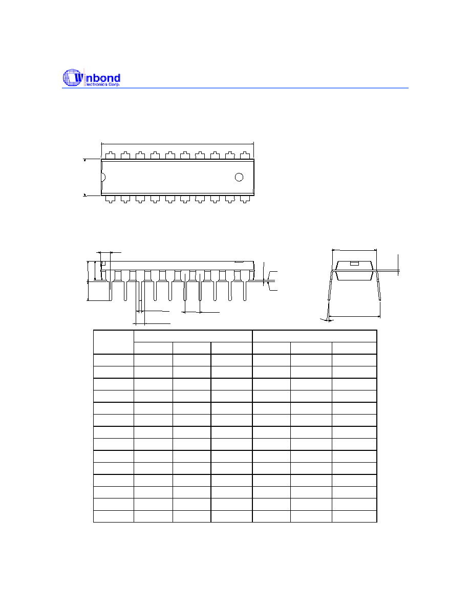
12. PACKAGE DRAWING AND DIMENSIONS ................................................................................... 31
12.1. 20L (PDIP) Plastic Dual Inline Package Dimensions (W682510 only)
......................... 31
12.2. 20L SSOP ≠ 209 mil Shrink Small Outline Package Dimensions
.................................. 32
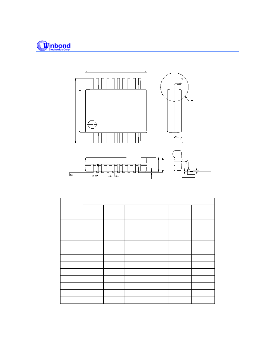
12.3. 24 SOP ≠ 300 mil
.................................................................................................................. 33
13. ORDERING INFORMATION........................................................................................................... 34
14. VERSION HISTORY........................................................................................................................ 35
Publication Release Date: May 2003
- 5 -
Revision 0.35
W682510/W682310
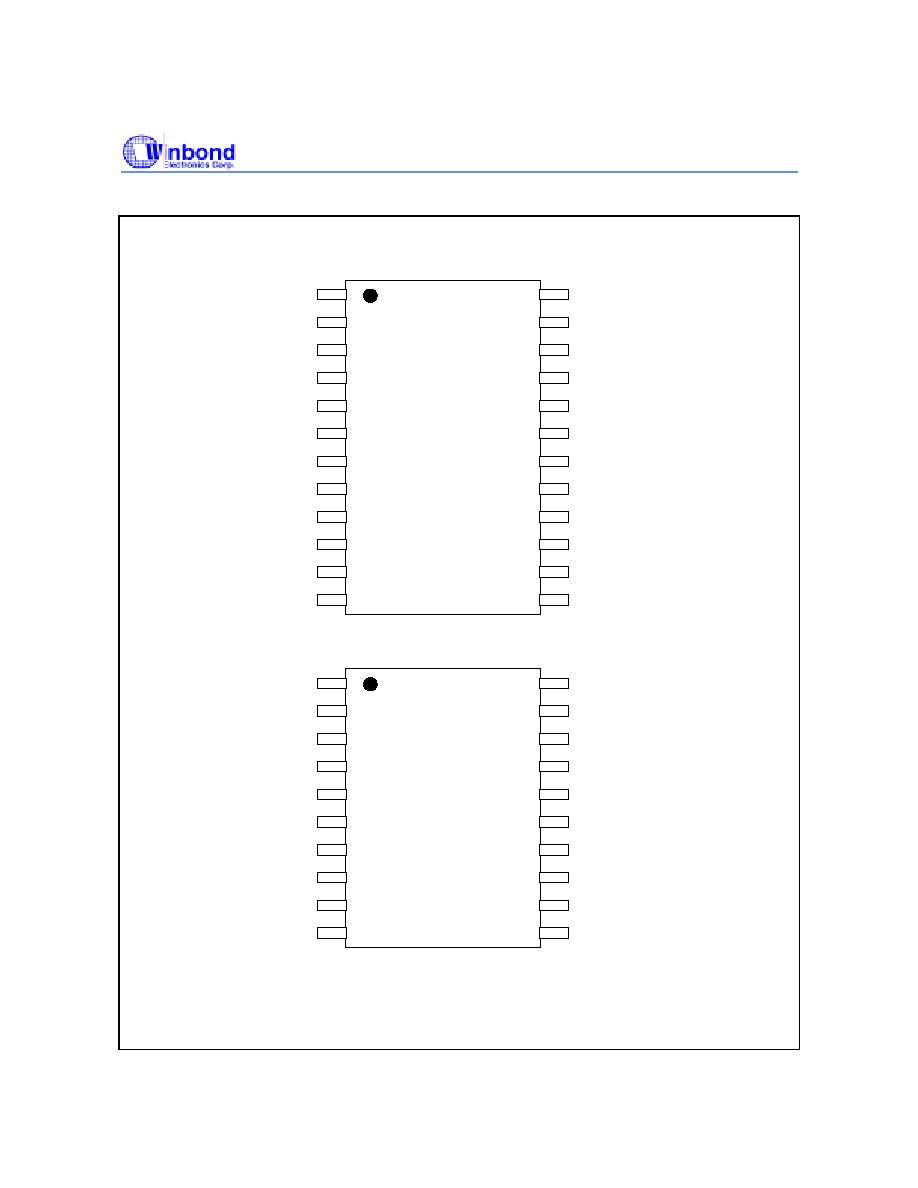
5. PIN CONFIGURATION
24
23
22
21
20
19
18
17
16
14
W682310
DUAL
CHANNEL
CODEC
1
2
3
4
5
6
7
8
9
11
SOP
V
REF
RO2
NC
RO1
PUI
PCMMS
NC
V
DD
V
SSD
FSR
PCMR2
PCMR1
AI2
AO2
-
AO1
-
AI1
NC
A-
µ/
Law
V
SSA
NC
BCLK
FST
PCMT2
PCMT1
10 15
12 13
20
19
18
17
16
15
14
13
12
W682310
DUAL
CHANNEL
CODEC
1
2
3
4
5
6
7
8
9
PDIP (W682510 only), SSOP
V
REF
RO2
RO1
PUI
PCMMS
V
DD
V
SSD
FSR
PCMR2
PCMR1
AI2
AO2
-
AO1
-
AI1
RO2
RO1
PUI
PCMMS
V
DD
V
SSD
FSR
PCMR2
PCMR1
AI2
AO2
-
AO1
-
AI1
A
µ/
-
Law
V
SSA
BCLK
FST
PCMT2
PCMT1
10 11
W682510/
W682510/
- 6 -

W682510/W682310
6. PIN DESCRIPTION
Pin
Name
Pin #
SSOP
PDIP
Pin #
SOP
Functionality
(CH1 = Channel 1, CH2 = Channel 2)
V
REF
1
1
This pin is used to bypass the signal ground. It needs to be decoupled to V
SS
through a 0.1
µ
F ceramic decoupling capacitor. No external loads should be
tied to this pin.
RO2
2
2
CH2 Non-Inverting output of the receive smoothing filter. This pin can typically
drive a 600
load (W682510) or 1200
load (W682310).
RO1
3
4
CH1 Non-Inverting output of the receive smoothing filter. This pin can typically
drive a 600
load (W682510) or 1200
load (W682310)..
PUI
4
5
Power up input signal. When this pin is HIGH (tied to V
DD
) the part is powered
up. When LOW (tied to V
SS
) the part is powered down.
PCMMS
5
6
PCM mode select input (serial or parallel data interface) HIGH = Parallel, LOW
= Serial
V
DD
6
8
Power supply. This pin should be decoupled to V
SS
with a 0.1
µ
F ceramic
capacitor.
V
SSD
7
9
This is the digital supply ground. This pin should be connected to 0V.
FSR
8
10
8 kHz Frame Sync input for the PCM receive section. It can also be connected
to the FST pin when transmit and receive are synchronous operations.
PCMR2
9
11
CH2 PCM input data receive pin. The data needs to be synchronous with the
FSR and BCLK pins.
PCMR1
10
12
CH1 PCM input data receive pin. The data needs to be synchronous with the
FSR and BCLK pins.
PCMT1
11
13
CH1 PCM output data transmit pin. The output data is synchronous with the
FST and BCLK pins.
PCMT2
12
14
CH2 PCM output data transmit pin. The output data is synchronous with the
FST and BCLK pins.
FST
13
15
8 kHz transmit frame sync input. This pin synchronizes the transmit data bytes.
BCLK
14
16
PCM transmit and receive bit clock input pin for CH1 and CH2 transmit.
V
SSA
15
18
This is the analog supply ground. This pin should be connected to 0V.
/A-Law
16
19
Compander mode select pin.
µ
-Law companding is selected when this pin is
LOW (tied to V
SS
.) A-Law companding is selected when pin is HIGH (tied to
V
DD
.)
AI1
17
21
CH1 Non-Inverting input of the first gain stage in the transmit path.
AO1-
18
22
CH1 Inverting analog output of the first gain stage in the transmit path.
AO2-
19
23
CH2 Inverting analog output of the first gain stage in the transmit path
AI2
20
24
CH2 Non-Inverting input of the first gain stage in the transmit path.
Publication Release Date: May 2003
- 7 -
Revision 0.35
W682510/W682310
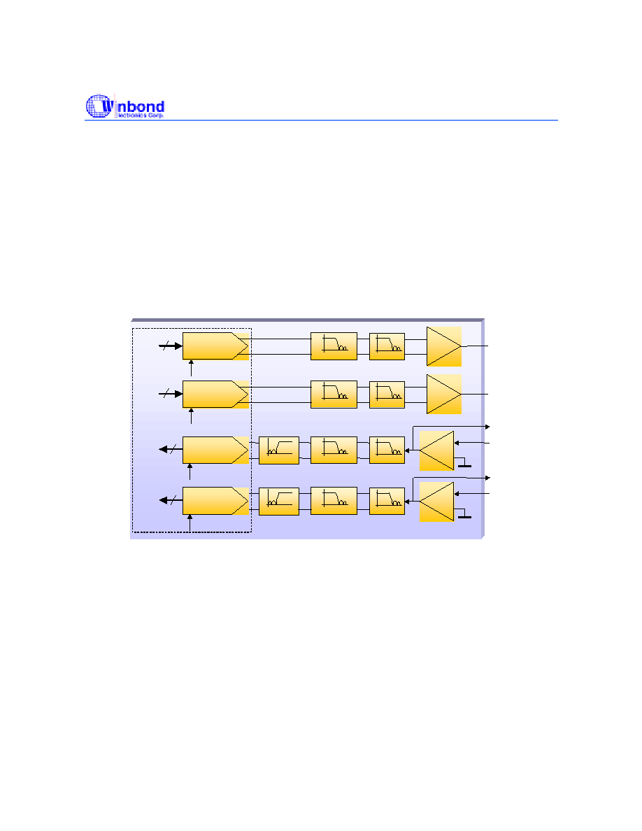
7. FUNCTIONAL DESCRIPTION
W682510/W682310 is a single-rail, dual channel PCM CODEC for voiceband applications. The
CODEC complies with the specifications of the ITU-T G.712 recommendation. The CODEC includes
two complete
µ
-Law and A-Law companders. The
µ
-Law and A-Law companders are designed to
comply with the specifications of the ITU-T G.711 recommendation.
The block diagram in section 3 shows the main components of the W682510/W682310. The chip
consists of a PCM interface, which can process the data in parallel or serial formats. The PLL of the
chip provides the internal clock signals and synchronizes the CODEC sample rate with the external
frame sync frequency. The power-conditioning block provides the internal power supply for the digital
and the analog section, while the voltage reference block provides a precision analog ground voltage
for the analog signal processing.
8
µ
/A
-
Control
8 bit
µ
/A
-
Law
DAC
RO1
-
+
Smoothing
Filter 1b
f
C
= 3400 Hz
Smoothing
Filter 1a
Buffer1
Av=1
DATA
R1
8
µ
/A
-
Control
8 bit
µ
/A
-
Law
DAC
RO2
-
+
Smoothing
Filter 2b
f
C
= 3400 Hz
Smoothing
Filter 2a
Buffer2
Av=1
DATA
R2
8
µ
/A
-
Control
AI2
AO2
-
-
+
Anti
-
Aliasin
Filter 2b
f
C
= 3400 Hz
Anti
-
Aliasin
Filter 2a
f
C
= 200 Hz
High Pass
Filter
8 bit
µ
/A
-
Law
ADC
DATA
T1
8
µ
/A
-
Control
AI1
AO1
-
-
+
Anti
-
Aliasin
Filter 1b
f
C
= 3400 Hz
Anti
-
Aliasin
Filter 1a
f
C
= 200 Hz
High Pass
Filter
8 bit
µ
/A
-
Law
ADC
DATA
T1
8
µ
/A
-
Control
8 bit
µ
/A
-
Law
DAC
RO1
-
+
Smoothing
Filter 1b
f
C
= 3400 Hz
Smoothing
Filter 1a
Buffer1
Av=1
DATA
R1
8
µ
/A
-
Control
8 bit
µ
/A
-
Law
DAC
RO1
-
+
Smoothing
Filter 1b
Smoothing
Filter 1b
f
C
= 3400 Hz
Smoothing
Filter 1a
f
C
= 3400 Hz
Smoothing
Filter 1a
Buffer1
Av=1
DATA
R1
8
µ
/A
-
Control
8 bit
µ
/A
-
Law
DAC
RO2
-
+
Smoothing
Filter 2b
Smoothing
Filter 2b
f
C
= 3400 Hz
Smoothing
Filter 2a
f
C
= 3400 Hz
Smoothing
Filter 2a
Buffer2
Av=1
DATA
R2
8
µ
/A
-
Control
AI2
AI2
AO2
-
-
+
Anti
-
Aliasing
Filter 2b
Anti
-
Filter 2b
f
C
= 3400 Hz
Anti
-
Aliasing
Filter 2a
f
C
= 3400 Hz
Anti
-
Filter 2a
f
C
= 200 Hz
High Pass
Filter
8 bit
µ
/A
-
Law
ADC
DATA
T2
8
µ
/A
-
Control
AI1
AI1
AO1
-
-
+
Anti
-
Aliasing
Filter 1b
Anti
-
Filter 1b
f
C
= 3400 Hz
Anti
-
Aliasing
Filter 1a
f
C
= 3400 Hz
Anti
-
Filter 1a
f
C
= 200 Hz
High Pass
Filter
8 bit
µ
/A
-
Law
ADC
DATA
T1
FIGURE 7.1: THE W682510 AND W682310 SIGNAL PATH
7.1. T
RANSMIT
P
ATH
The A-to-D path of the CODEC contains an analog input amplifier with externally configurable gain
setting (see application examples in section 11). The transmit amplifier output is the input to the
encoder section.
The output of the input amplifier is fed through a low-pass filter to prevent aliasing at the switched
capacitor 3.4 kHz low pass filter. The 3.4 kHz switched capacitor low pass filter prevents aliasing of
input signals above 4 kHz, due to the sampling at 8 kHz. The output of the 3.4 kHz low pass filter is
filtered by a high pass filter with a 200 Hz cut-off frequency. The filters are designed according to the
recommendations in the G.712 ITU-T specification. From the output of the high pass filter the signal is
digitized. The signal is converted into a compressed 8-bit digital representation with either
µ
-Law or A-
- 8 -

W682510/W682310
Law format. The
µ
-Law or A-Law format is pin-selectable through the
µ
/A-Law pin. The compression
format can be selected according to Table 7.1.
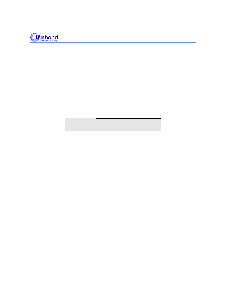
TABLE 7.1: PIN-SELECTABLE COMPRESSION FORMAT
µ
/A-Law Pin
Format
V
DD
(HIGH)
A-Law
V
SSA
(LOW)
µ
-Law
The digital 8-bit
µ
-Law or A-Law samples are fed to the PCM interface for serial or parallel
transmission at the sample rate supplied by the external frame sync FST.
7.1.1. AI1, AI2, AO1-, AO2-
AI1 and AI2 are the transmit analog inputs for channels 1 and 2. AO1- and AO2- are the transmit level
feedback for channels 1 and 2. AI1 and AI2 are inverting inputs for the Op-Amps. AO1- and AO2- are
connected to the outputs of the Op-Amps and are used to set the level, as illustrated below. When AI1
and AI2 are not used, connect AI1 to AO1- and AI2 to AO2-. During power saving mode and power
down mode, the AO1- and AO2- outputs are tied weakly to V
SSA
on the W682510 or are high
impedance on the W682310 (See table on page 14).
AO1
-
AI1
-
+
C1
R1
R2
AO2
-
AI2
-
+
C2
R3
R4
CH1 Analog Input
CH2 Analog Input
Gain=R2/R1
10
R2 > 20 k Ohm
Gain=R4/R3
10
R4 > 20 k Ohm
AO1
-
AI1
-
+
C1
R1
R2
AO2
-
AI2
-
+
C2
R3
R4
AO1
-
AI1
-
+
C1
R1
R2
AO1
-
AI1
-
+
C1
R1
R2
AO2
-
AI2
-
+
C2
R3
R4
AO2
-
AI2
-
+
C2
R3
R4
CH1 Analog Input
CH2 Analog Input
Gain=R2/R1
10
R2 > 20 k Ohm
Gain=R4/R3
10
R4 > 20 k Ohm
7.1.2. PCMT1
The PCM signal output of channel 1 when the parallel mode is selected. The PCM output signal is
sent from PCMT1 in a sequential order, synchronizing with the rising edge of the BCLK signal. The
MSB may be output at the rising edge of the FST signal, based on the timing between BCLK and FST.
This output pin is in a high impedance state except during 8-bit PCM output. It is also in a high
impedance state during power-saving state or power-down. When serial operation is selected, this pin
is configured to be the output of the serial multiplexed two channel PCM signal. A pull-up resistor must
Publication Release Date: May 2003
- 9 -
Revision 0.35
W682510/W682310
be connected to this pin , as it is an open drain output. This device is compatible with the ITU-T coding
law and output coding format recommendation.
TABLE 7.15: PCM CODES FOR ZERO AND FULL SCALE
µ
-Law
A-Law
Level
Sign bit
Chord bits
Step bits
Sign Bit
Chord Bits
Step Bits
+ Full Scale
1
000
0000
1
010
1010
+
Zero
1 111 1111 1 101 0101
-
Zero
0 111 1111 0 101 0101
- Full Scale
0
000
0000
0
010
1010
7.1.3. PCMT2
The PCM signal output for channel 2 when the parallel mode is selected. The PCM output signal is
sent from PCMT2 in a sequential order, synchronized with the rising edge of the BCLK signal. The
MSB may be output at the rising edge of the FST signal, based on the timing between BCLK and FST.
This pin is in a high impedance state except during 8-bit PCM output. It is also in a high impedance
state during power-saving state or power-down. When the serial operation is selected, this pin is left
open. A pull-up resistor must be connected to this pin , as it is an open drain output. This device is
compatible with the ITU-T coding law and output coding format recommendation.
7.2. R
ECEIVE
P
ATH
The 8-bit digital input samples for the D-to-A path are serially shifted in by the PCM interface and
converted to parallel data bits. During every cycle of the frame sync FSR, the parallel data bits are fed
through the pin-selectable
µ
-Law or A-Law expander and converted to analog samples. The mode of
expansion is selected by the
µ
/A-Law pin as shown in Table 7.2. The analog samples are filtered by a
low-pass smoothing filter with a 3.4 kHz cut-off frequency, according to the ITU-T G.712 specification.
A sin(x)/x compensation is integrated with the low pass smoothing filter. The output of this filter is
buffered to provide the receive output signal RO.
7.2.1. RO1, RO2
RO1 and RO2 are the receive analog outputs for channel 1 and channel 2. The output signal of the
W682510 has an amplitude of 3.46 Vpp (2.03 Vpp for W682310) around the signal ground voltage
(V
REF
). When the digital PCM signal of +3 dBm0 is presented to PCMR1 or PCMR2, it can drive a load
of 600 Ohms or more at 5 V supply voltage for the W682510 and 1200 Ohms at 3V supply for the
W682310. During power saving mode, these outputs are at the voltage level of V
REF
with a high
impedance. These outputs have a feature that reduces audio "pop" noises when switching between
active and inactive states and back.
- 10 -

W682510/W682310
7.2.2. PCMR1
The PCM signal input for channel 1 when in the parallel mode. D/A conversion is performed on the
serial PCM signal input to this pin. The FSR signal, synchronous with the serial PCM signal, and the
BCLK signal, processes the code. Then the analog output is output from the RO1 pin. The data rate of
the PCM signal is equal to the frequency of the BCLK signal.
The PCM signal is shifted in on the falling edge of the BCLK signal. It is latched into the internal 8-bit
register. The start of the PCM data (MSB) is synchronized with the rising edge of FSR. In the serial
mode, this pin is not used and should be connected to GND (0V).
7.2.3. PCMR2
PCM signal input for channel 2 when the parallel mode is selected. D/A conversion is performed with
the serial PCM signal input to this pin, the FSR signal, synchronous with the serial PCM signal, and
the BCLK signal, and then the analog output is output from the RO2 pin. The data rate of the PCM
signal is equal to the frequency of the BCLK signal. The PCM signal is shifted at the falling edge of the
BCLK signal and latched into the internal register when shifted by eight bits. The start of the PCM data
(MSB) is identified at the rising edge of FSR. In the serial mode this pin is used for the two channel
multiplexed PCM signal input.
7.3. P
OWER
S
IGNALS
7.3.1. V
DD
The power supply for the analog and digital parts of the W682510 must be 5V +/- 10% and 2.7V to
3.8V for the W682310. This supply voltage is connected to the V
DD
pin. The V
DD
pin needs to be
decoupled to ground through a 0.1
µ
F ceramic capacitor. A power supply for an analog circuit in the
system to which the device is applied should be used. A bypass capacitor of 0.1 µF to 1 µF with good
high-frequency characteristics (Low ESR) and a capacitor of 10 µF to 20 µF should be connected
between this pin and the V
SSA
pin if needed.
7.3.2. V
SSA
Ground for the analog signal circuits. This ground is separate from the digital signal ground. The V
SSA
pin must be connected to the V
SSD
pin on the printed circuit board to make a common ground.
However, it's advised to connect the PCB traces of these pins at the main supply hookup of the PCB
and run the V
SSA
and V
SSD
traces separately to the device.
7.3.3. V
SSD
Ground for the digital signal circuits. This ground is separate from the analog signal ground. The V
SSD
pin must be connected to the V
SSA
pin on the printed circuit board to make a common ground.
However, it's advised to connect the PCB traces of these pins at the main supply hookup of the PCB
and run the V
SSA
and V
SSD
traces separately to the device
Publication Release Date: May 2003
- 11 -
Revision 0.35
W682510/W682310
7.3.4. V
REF
This pin carries the signal ground voltage level and requires a bypass capacitor. A 0.1
µ
F ceramic
(with low ESR for good high frequency response) capacitor needs to be connected between the V
SSA
pin and the V
REF
pin.
7.3.5. PUI
Power up input signal. When the PUI pin is set to logic "0" level, the CODEC will go into power down
mode.
7.4. PCM I
NTERFACE
The PCM interface is controlled by pins PCMMS, BCLK, FSR & FST. The input data is received
through the PCMR pin and the output data is transmitted through the PCMT pin. The modes of
operation of the interface are shown in Table 7.2.
TABLE 7.2: PCM INTERFACE MODE SELECTIONS
PCMMS
PCM Mode
Data Available
V
DD
[HIGH]
Parallel
Mode
CH1 data on PCMT1 & PCMR1
CH2 data on PCMT2 and PCMR2 (same timing as CH1)
V
SS
[LOW]
Serial Mode
CH1 data followed by CH2 receive data on PCMR2 (total 16 bits)
CH1 data followed by CH2 transmit data on PCMT1 (total 16 bits)
7.4.1.
µ
/A-Law
This pin selects the desired companding law. The CODEC will operate in the
µ
-law when this pin is at
a logic "0" level and in the A-law when at a logic "1" level. The CODEC operates
µ
-law if the pin is left
open, since this pin is internally pulled down.
TABLE 7.25: PIN-SELECTABLE COMPRESSION FORMAT
µ
/A-Law pin
Format
HIGH (V
DD
) A-Law
LOW (V
SS
), Floating
µ
-Law
- 12 -

W682510/W682310
7.4.2. BCLK
This is the shift clock signal input for the PCMR1, PCMR2, PCMT1, and PCMT2 signals. The
frequency, equal to the data rate, is 64, 96, 128, 192, 256, 384, 512, 768, 1024, 1536, 1544, 2048 or
200 kHz. Setting this signal to a steady logic "1" or "0" sets both transmit and receive circuits to the
power saving state.
7.4.3. FSR
This is the receive synchronizing signal input. The required eight-bits of PCM data are selected from
the PCM data signal to the PCMR1 and PCMR2 pins by the receive synchronizing signal. All timing
signals in the receive section are synchronized by this synchronizing signal. This signal must be in
phase with the BCLK. The frequency should be 8 kHz
±
50 ppm to guarantee the AC characteristics.
This device can operate in the range of 6 kHz to 9 kHz, but the electrical characteristics specified in
the data sheet are not guaranteed.
7.4.4. FST
The transmit synchronizing signal input. The PCM output signal from PCMT1 and PCMT2 is sent in
synchronization with this transmit synchronizing signal. This FST signal triggers the PLL and
synchronizes all timing signals of the transmit section. The synchronizing signal must be in phase with
BCLK. The frequency should be 8 kHz
±
50 ppm to guarantee the AC characteristics. This device can
operate in the range of 6 kHz to 9 kHz sample rates, but the electrical characteristics are not
guaranteed. Setting this signal to logic HIGH or LOW drives both transmit and receive circuits to
power saving state.
7.4.5. PCMMS
The control signal for mode selection of the PCM input and output. When this signal is HIGH, the PCM
input and output are in the parallel mode. The PCM data of CH1 and CH2 is input to PCMR1 and
PCMR2, and output from PCMT1 and PCMT2, with the same timing. When this signal is at a LOW
level, the PCM input and output are in the serial mode. The PCM data of CH1 and CH2 is input to
PCMR2 and output from PCMT1 as two serial 8-bit bytes.
7.5. P
OWER
S
TATE
M
ODES
7.5.1. Power Save Mode
In the power save mode, all internal analog circuits except the internal reference are powered down.
The CODEC automatically enters the power save mode when the FST or BCLK signal is set to digital
"1" or digital "0";
Upon power up with FST and BCLK signals present, it will take 2 to 10 milliseconds for the internal
PLL to lock. In addition to the PLL lock-in time, the analog outputs will be set to the internal signal
ground for 1 millisecond. This will avoid power up glitches at the outputs. The digital open drain
outputs will remain at high impedance during this power up delay.
Publication Release Date: May 2003
- 13 -
Revision 0.35
W682510/W682310
7.5.2. Power Down Mode
When the power up indicator pin, PUI, is set LOW all internal circuits will go into the power down state.
It will take 2 to 10 milliseconds for the PLL to lock when operation is resumed with the FST and BCLK
signals applied and PUI set HIGH. An additional 1-millisecond delay is used to set the analog outputs
to the signal ground reference in order to avoid power up glitches. The digital open drain outputs will
remain at high impedance during this power up delay.
7.5.3. Power Save/Down Output pin state
The following table shows the states of the output pins in the power save or power down mode.
TABLE 7.5: OUTPUT PIN STATES
Output Pin
Product Name
AO1-, A02-
RO1, RO2
W682510 V
SSA
Signal
Ground
W682310
High Z
Signal Ground
- 14 -

W682510/W682310
8. TIMING DIAGRAMS
Figure 8-1a. Transmit Side Serial Mode Timing (PCMMS=0)
FST
PCMT1
D0
D1
D2
D3
D4
D5
D6
MSB
D0
D1
D2
D3
D4
D5
D6
MSB
BCLK
Figure 8-1b. Receive Side Serial Mode Timing (PCMMS=0)
FSR
PCMR2
D0
D1
D2
D3
D4
D5
D6
MSB
D0
D1
D2
D3
D4
D5
D6
MSB
BCLK
Channel 1 Transmit PCM Data
Channel 2 Transmit PCM Data
Channel 2 Receive PCM Data
Channel 1 Receive PCM Data
FIGURE 8.1: SERIAL MODE PCM TIMING
Figure 8-2a. Transmit Side Parallel Mode Timing (PCMMS=1)
FST
PCMT1
PCMT2
D0
D1
D2
D3
D4
D5
D6
MSB
BCLK
Figure 8-2b. Receive Side Parallel Mode Timing (PCMMS=1)
FSR
PCMR1
PCMR2
D0
D1
D2
D3
D4
D5
D6
MSB
BCLK
FIGURE 8.2: PARALLEL MODE PCM TIMING
Publication Release Date: May 2003
- 15 -
Revision 0.35

W682510/W682310
Figure 8-3a. Burst Mode with Serial Timing (PCMMS=0)
FST
FSR
PCMT1
PCMR2
D0
D1
D2
D3
D4
D5
D6
MSB
D0
D1
D2
D3
D4
D5
D6
MSB
BCLK
Figure 8-3b. Burst Mode with Parallel Timing (PCMMS=1)
FST
FSR
PCMTx
PCMRx
D0
D1
D2
D3
D4
D5
D6
MSB
BCLK
Channel 1 PCM Data
Channel 2 PCM Data
1 2 3 4 5 6 7 8 9
1 2 3 4 5 6 7 8 9
10 11 12 13 14 15 16 17
FIGURE 8.3: BURST MODE PCM TIMING
- 16 -

W682510/W682310
TABLE 8.1: PCM SYNCHRONIZATION PARAMETERS
SYMBOL
DESCRIPTION
MIN
TYP
MAX UNIT
f
FS
FST, FSR frequency
---
8 --- KHz
t
WS
FST, FSR Pulse Width
1
---
7
T
BCLK
t
j
FST, FSR allowable jitter
0
---
500
nsec
f
BCLK
BCLK frequency
64, 128, 256, 512,
1024, 2048, 96, 192,
384, 768, 1536,
1544, 200
kHz
D
C
BCLK
Duty
Cycle
40 50 60 %
t
Ir
FSR, FST, BCLK, PCMR1, PCMR2, PUI, PCMMS
input rise time
--- --- 50 nsec
t
If
FSR, FST, BCLK, PCMR1, PCMR2, PUI, PCMMS
input fall time
--- --- 50 nsec
BCLK
t
WS
8
7
6
5
4
3
2
1
FSR
FST
t
j
T
BCLK
=1/f
BCLK
T
FS
=1/f
FS
D
C
t
Ir
t
If
FIGURE 8.4: PCM SYNCHRONIZATION PARAMETERS
Publication Release Date: May 2003
- 17 -
Revision 0.35

W682510/W682310
TABLE 8.2: PCM TIMING PARAMETERS
SYMBOL
DESCRIPTION
MIN
TYP
MAX UNIT
t
WS
FST, FSR Pulse Width
T
BCLK
---
100
µ
sec
t
XS
BCLK low to FST high setup time
100
---
---
nsec
t
SX
FST high to BCLK low hold time
100
---
---
nsec
t
SD
PCMT1, PCMT2 output delay; Cl = 100 pF
20
---
200
nsec
t
XD1
PCMT1, PCMT2 output delay; Cl = 100 pF
20
---
200
nsec
t
XD2
PCMT1, PCMT2 output delay; Cl = 100 pF
20
---
200
nsec
t
XD3
PCMT1, PCMT2 output delay; Cl = 100 pF
20
---
200
nsec
t
RS
BCLK low to FSR high setup time
100
---
---
nsec
t
SR
FSR high to BCLK low hold time
100
---
---
nsec
t
DS
PCMR1, PCMR2 Data in setup time
100
---
---
nsec
t
DH
PCMR1, PCMR2 Data in hold time
100
---
---
nsec
R
TL
PCMT1, PCMT2 Pull-up resistor
500
---
---
Ohm
C
TL
PCMT1, PCMT2 Load capacitance
---
---
100
pF
Figure 8-5a. Transmit Timing
FST
PCMT1
PCMT2
BCLK
MSB
D0
D1
D2
D3
D4
D5
D6
t
WS
t
SX
t
XS
t
XD1
t
SD
t
XD2
t
XD3
Figure 8-5b. Receive Timing
FSR
PCMR1
PCMR2
BCLK
11
MSB
D0
D1
D2
D3
D4
D5
D6
t
WS
t
SR
t
RS
t
DH
t
DS
10
9
8
7
6
5
4
3
2
1
11
10
9
8
7
6
5
4
3
2
1
FIGURE 8.5 PCM TIMING PARAMETERS
- 18 -

W682510/W682310
9. ABSOLUTE MAXIMUM RATINGS
TABLE 9.1: ABSOLUTE MAXIMUM RATINGS (PACKAGED PARTS)
Condition
Value
Junction temperature
150
0
C
Storage temperature range
-65
0
C to +150
0
C
Voltage Applied to any pin
(V
SS
- 0.3V) to (V
DD
+ 0.3V)
Voltage applied to any pin (Input current limited to +/-20 mA)
(V
SS
≠ 1.0V) to (V
DD
+ 1.0V)
Lead temperature (soldering ≠ 10 seconds)
300
0
C
V
DD
- V
SS
-0.5V to +6V
Note
: Exposure to conditions beyond those listed under Absolute Maximum Ratings may adversely
affect the life and reliability of the device. Functional operation is not implied at these
conditions.
TABLE 9.2: OPERATING CONDITIONS (PACKAGED PARTS)
Condition
Value
Industrial operating temperature
-40
0
C to +85
0
C
Supply voltage (V
DD
) W682510 5V
+4.5V to +5.5V
Supply voltage (V
DD
) W682310 3V
+2.7V to +3.8V
Ground voltage (V
SS
) 0V
Publication Release Date: May 2003
- 19 -
Revision 0.35
W682510/W682310
10. ELECTRICAL CHARACTERISTICS
10.1. G
ENERAL
P
ARAMETERS
W682510 4.5V
≠ 5.5V
Symbol Parameters
Conditions
Min
(2)
Typ
(1)
Max
(2)
Units
V
IL
Input Low Voltage
0.0
0.8
V
V
IH
Input High Voltage
2.2
V
DD
V
V
OL
PCMT1, PCMT2 Output
Low Voltage
R
pullup
>500
0.0 0.2 0.4 V
I
DD
V
DD
Current (Operating) -
ADC + DAC
No Load, No Signal
7 14
mA
I
SB
V
DD
Current (Standby)
FST or BCLK =OFF; PUI=V
DD
800 1300
µ
A
I
PD
V
DD
Current (Power Down) PUI= V
ss
1
10
µ
A
I
IL
Input Low Leakage Current
V
SS
<V
IN
<V
DD
0.5
µ
A
I
IH
Input High Leakage Current V
SS
<V
IN
<V
DD
2
µ
A
I
OL
PCMT1, PCMT2 Output
Leakage Current
V
SS
<PCMT<V
DD
High Z State
+/-10
µ
A
C
IN
Digital Input Capacitance
5
10
pF
C
OUT
PCMT1, PCMT2 Output
Capacitance
PCMT1, PCMT2 = High Z
15
pF
1. Typical values: T
A
= 25∞C,
V
DD
= 5.0 V
2. All min/max limits are guaranteed by Winbond via electrical testing or characterization. Not all
specifications are 100 percent tested.
10.2. G
ENERAL
P
ARAMETERS
W682310 2.7V ≠ 3.8V
Symbol Parameters
Conditions
Min
(2)
Typ
(1)
Max
(2)
Units
V
IL
Input Low Voltage
0.0
0.16xV
DD
V
V
IH
Input High Voltage
0.45xV
DD
V
DD
V
V
OL
PCMT1, PCMT2 Output
Low Voltage
R
pullup
>500
0.0 0.2 0.4 V
I
DD
V
DD
Current (Operating) -
ADC + DAC
No Load, No Signal
7.4 14 mA
I
SB
V
DD
Current (Standby)
FST or BCLK =OFF; PUI=V
DD
700 2000
µ
A
I
PD
V
DD
Current (Power Down) PUI= V
ss
1
10
µ
A
I
IL
Input Low Leakage Current
V
SS
<V
IN
<V
DD
0.5
µ
A
- 20 -

W682510/W682310
Symbol Parameters
Conditions
Min
(4)
Typ
(3)
Max
(4)
Units
I
IH
Input High Leakage Current V
SS
<V
IN
<V
DD
2
µ
A
I
OL
PCMT1, PCMT2 Output
Leakage Current
V
SS
<PCMT<V
DD
High Z State
+/-10
µ
A
C
IN
Digital Input Capacitance
5
10
pF
C
OUT
PCMT1, PCMT2 Output
Capacitance
PCMT1, PCMT2 = High Z
15
pF
1. Typical values: T
A
= 25∞C,
V
DD
= 3.0 V
2. All min/max limits are guaranteed by Winbond via electrical testing or characterization. Not all
specifications are 100 percent tested.
Publication Release Date: May 2003
- 21 -
Revision 0.35

W682510/W682310
10.3. A
NALOG
S
IGNAL
L
EVEL AND
G
AIN
P
ARAMETERS
W682510: V
DD
=5V
±
10%; V
SS
=0V; T
A
=-40
∞
C to +85
∞
C; all analog signals referred to V
REF
;
W682310: V
DD
=2.7V to 3.8V; V
SS
=0V; T
A
=-40
∞
C to +85
∞
C; all analog signals referred to V
REF
;
TRANSMIT (A/D) RECEIVE (D/A)
UNIT
PARAMETER
SYM.
CONDITION
TYP.
MIN.
MAX.
MIN.
MAX.
Reference Level
Out
W682510 5V
L
ABS
0 dBm0 = +0.8 dBm @
600
load 1020 Hz
0.850
--- --- --- --- V
RMS
Reference Level
In
W682510 5V
T
0TLP
1020
Hz
0.850
--- --- --- --- V
RMS
Reference Level
Out
W682310 3V
L
ABS
0 dBm0 = -3.8 dBm @
1200
load 1020 Hz
0.500
--- --- --- --- V
RMS
Reference Level
Out
W682310 3V
T
0TLP
1020
Hz
0.350
--- --- --- --- V
RMS
Max. Transmit
Level In
W682510 5V
T
XMAX
3.17 dBm0 for
µ
-Law
3.14 dBm0 for A-Law
1.732
1.726
---
---
---
---
---
---
---
---
V
PK
V
PK
Max. Transmit
Level In
W682310 3V
T
XMAX
3.17 dBm0 for
µ
-Law
3.14 dBm0 for A-Law
0.712
0.708
---
---
---
---
---
---
---
---
V
PK
V
PK
Absolute Gain
(0 dBm0 @
1020 Hz;
T
A
=+25
∞
C)
G
ABS
0 dBm0 @ 1020 Hz;
T
A
=+25
∞
C
0
-0.2 +0.2 -0.2 +0.2 dB
Absolute Gain
variation with
Temperature
G
ABST
T
A
=0
∞
C to T
A
=+70
∞
C
T
A
=-40
∞
C to T
A
=+85
∞
C
0 -0.08
-0.1
+0.08
+0.1
-0.08
-0.1
+0.08
+0.1
dB
Frequency
Response,
Relative to
0dBm0 @ 1020
Hz
G
RTV
15
Hz
50 Hz
60 Hz
200 Hz
300 to 3000 Hz
3300 Hz
3400 Hz
3600 Hz
4000 Hz
4600 Hz to 100 kHz
---
---
---
---
---
---
---
---
---
---
---
---
---
-1.5
-0.20
-0.50
-0.8
---
---
---
-40
-30
-20
-0.4
+0.20
+0.20
0
0
-14
-32
-0.5
-0.5
-0.5
-0.5
-0.20
-0.50
-0.8
---
---
---
0
0
0
0
+0.20
+0.20
0
0
-14
-30
dB
- 22 -

W682510/W682310
Gain Variation
vs. Level Tone
(1020 Hz
relative to ≠10
dBm0)
G
LT
+3 to ≠40 dBm0
-40 to ≠50 dBm0
-50 to ≠55 dBm0
---
---
---
-0.3
-0.5
-1.2
+0.3
+0.5
+1.2
-0.3
-0.5
-1.2
+0.3
+0.5
+1.2
DB
Publication Release Date: May 2003
- 23 -
Revision 0.35

W682510/W682310
10.4. A
NALOG
D
ISTORTION AND
N
OISE
P
ARAMETERS
W682510: V
DD
=5V
±
10%; V
SS
=0V; T
A
=-40
∞
C to +85
∞
C; all analog signals referred to V
REF
;
W682310: V
DD
=2.7V to 3.8V; V
SS
=0V; T
A
=-40
∞
C to +85
∞
C; all analog signals referred to V
REF
;
TRANSMIT (A/D)
RECEIVE (D/A)
PARAMETER
SYM.
CONDITION
MIN.
TYP. MAX.
MIN.
TYP. MAX.
UNIT
Total Distortion vs.
Level Tone (1020 Hz,
µ
-Law, C-Message
Weighted)
D
LT
µ
+3 dBm0
0 dBm0 to -30 dBm0
-40 dBm0
-45 dBm0
36
36
29
25
---
---
---
---
---
---
---
---
34
36
30
25
---
---
---
---
---
---
---
---
dBC
Total Distortion vs.
Level Tone (1020 Hz,
A-Law, Psophometric
Weighted)
D
LTA
+3
dBm0
0 dBm0 to -30 dBm0
-40 dBm0
-45 dBm0
36
36
29
25
---
---
---
---
---
---
---
---
34
36
30
25
---
---
---
---
---
---
---
---
dBp
Spurious Out-Of-Band
at RO- (300 Hz to
3400 Hz @ 0dBm0)
D
SPO
4600 Hz to 7600 Hz
7600 Hz to 8400 Hz
8400 Hz to 100000 Hz
---
---
---
---
---
---
---
---
---
---
---
---
---
---
---
-30
-40
-30
dB
Spurious In-Band (700
Hz to 1100 Hz @
0dBm0)
D
SPI
300 to 3000 Hz
---
--- -47
---
--- -47
dB
Intermodulation
Distortion (300 Hz to
3400 Hz ≠4 to ≠21
dBm0
D
IM
Two
tones
--- --- -41 --- --- -41 dB
Crosstalk (1020 Hz @
0dBm0)
D
XT
--- --- -75 --- --- -75 dBm0
Channel to Channel
Crosstalk (1020 Hz @
0dBm0)
D
XTCH
--- --- -75 --- --- -75 dBm0
Absolute Group Delay
ABS
1600
Hz
--- --- 360
--- --- 240
µ
sec
Group Delay
Distortion (relative to
group delay @ 1200
Hz)
D
500 Hz
600 Hz
1000 Hz
2600 Hz
2800 Hz
---
---
---
---
---
---
---
---
---
---
750
380
130
130
750
---
---
---
---
---
---
---
---
---
---
750
370
120
120
750
µ
sec
Idle Channel Noise
N
IDL
µ
-Law; C-message
A-Law; Psophometric
---
---
---
---
5
-69
---
---
---
---
13
-79
dBrnc
dBm0p
- 24 -

W682510/W682310
10.5. A
NALOG
I
NPUT AND
O
UTPUT
A
MPLIFIER
P
ARAMETERS
W682510: V
DD
=5V
±
10%; V
SS
=0V; T
A
=-40
∞
C to +85
∞
C; all analog signals referred to V
REF
;
W682310: V
DD
=2.7V to 3.8V; V
SS
=0V; T
A
=-40
∞
C to +85
∞
C; all analog signals referred to V
REF
;
PARAMETER
SYM.
CONDITION
MIN.
TYP.
MAX.
UNIT.
AI1, AI2 Input Offset Voltage
V
OFF,AI
Unity
Gain
---
---
±
20
mV
AI1, AI2 Input Resistance
R
IN,AI
AI1, AI2 to V
REF
10
---
---
M
AO1-, AO2- Output Amplitude
V
AD
W682510
W682310
0 ---
3.4
1.4
Vpp
AO1-, AO2- Load Resistance
R
LOAD
20
--- ---
k
AO1-, AO2- Load Capacitance
C
LOAD
AO1-,
AO2-
---
--- 30
pF
RO1, RO2 Load Resistance
R
LOAD
W682510
W682310
0.6
1.2
--- ---
k
RO1, RO2 Load Capacitance
C
LOAD
RO1,
RO2
---
--- 50
pF
RO1, RO2 Output Amplitude
V
ORO
W682510
W682310
--- ---
3.4
2.0
Vpp
RO1, RO2 Output Offset Voltage
V
OFF,RO
RO to V
REF
---
---
±
100
mV
Signal Ground Voltage to V
SSA
V
REF
V
DD
/2 ≠ 0.1
V
DD
/2
V
DD
/2+ 0.1 V
Power Supply Rejection Ratio (0 to
100 kHz to V
DD
, C-message)
PSRR
Transmit; 50 mVpp
Receive; 50 mVpp
--
--
40
40
---
---
dBC
Publication Release Date: May 2003
- 25 -
Revision 0.35

W682510/W682310
10.6. D
IGITAL
I/O
TABLE 10.61:
µ
-LAW ENCODE DECODE CHARACTERISTICS
Digital Code
D7 D6 D5 D4 D3 D2 D1 D0
Normalized
Encode
Decision
Levels
Sign Chord Chord Chord Step Step Step Step
Normalized
Decode
Levels
1 0 0 0 0 0 0 0 8031
:
1 0 0 0 1 1 1 1 4191
:
1 0 0 1 1 1 1 1 2079
:
1 0 1 0 1 1 1 1 1023
:
1 0 1 1 1 1 1 1 495
:
1 1 0 0 1 1 1 1 231
:
1 1 0 1 1 1 1 1 99
:
1 1 1 0 1 1 1 1 33
:
1 1 1 1 1 1 1 0 2
1 1 1 1 1 1 1 1 0
8159
7903
:
4319
4063
:
2143
2015
:
1055
991
:
511
479
:
239
223
:
103
95
:
35
31
:
3
1
0
Notes:
Sign bit = 0 for negative values, sign bit = 1 for positive values
- 26 -

W682510/W682310
TABLE 10.62: A-LAW ENCODE DECODE CHARACTERISTICS
Digital Code
D7 D6 D5 D4 D3 D2 D1 D0
Normalized
Encode
Decision
Levels
Sign Chord Chord Chord Step Step Step Step
Normalized
Decode
Levels
1 0 1 0 1 0 1 0 4032
:
1 0 1 0 0 1 0 1 2112
:
1 0 1 1 0 1 0 1 1056
:
1 0 0 0 0 1 0 1 528
:
1 0 0 1 0 1 0 1 264
:
1 1 1 0 0 1 0 1 132
:
1 1 1 0 0 1 0 1 66
:
1 1 0 1 0 1 0 1 1
4096
3968
:
2048
2048
:
1088
1024
:
544
512
:
272
256
:
136
128
:
68
64
:
2
0
Notes:
1. Sign bit = 0 for negative values, sign bit = 1 for positive values
2. Digital code includes inversion of all even number bits
Publication Release Date: May 2003
- 27 -
Revision 0.35

W682510/W682310
TABLE 10.63: PCM CODES FOR ZERO AND FULL SCALE
µ
-Law
A-Law
Level
Sign bit
(D7)
Chord bits
(D6,D5,D4)
Step bits
(D3,D2,D1,D0)
Sign bit
(D7)
Chord bits
(D6,D5,D4)
Step bits
(D3,D2,D1,D0)
+ Full Scale
1
000
0000
1
010
1010
+ Zero
1
111
1111
1
101
0101
- Zero
0
111
1111
0
101
0101
- Full Scale
0
000
0000
0
010
1010
TABLE 10.64: PCM CODES FOR 0DBM0 OUTPUT
µ
-Law
A-Law
Sample
Sign bit
(D7)
Chord bits
(D6,D5,D4)
Step bits
(D3,D2,D1,D0)
Sign bit
(D7)
Chord bits
(D6,D5,D4)
Step bits
(D3,D2,D1,D0)
1 0
001
1110
0
011
0100
2 0
000
1011
0
010
0001
3 0
000
1011
0
010
0001
4 0
001
1110
0
011
0100
5 1
001
1110
1
011
0100
6 1
000
1011
1
010
0001
7 1
000
1011
1
010
0001
8 1
001
1110
1
011
0100
- 28 -

W682510/W682310
11. TYPICAL APPLICATION CIRCUIT
0.1
µ
F
1
µ
F
V
DD
Bit Clock Input
PCM 2 Ch. Serial Output
1k
AI2 24
AO2
-
23
AO1
-
22
AI1 21
NC 20
W682510/W2310
1 VREF
2 RO2
3 NC
4 RO1
5 PUI
6 PCMMS
7 NC
8 V
DD
9 V
SSD
11 PCMR2
SOP
10 FSR
12 PCMR1
A/
µ
19
V
SSA
18
NC 17
BCLK 16
PCMT2 14
FST 15
PCMT1 13
PCMT1 13
Channel
Analog
Input
Channel
Analog
Input
Channel 2
Analog
Output
Channel 1
Analog
Output
Power Up
Input
Frame Sync Input
PCM 2 Ch Serial Input
V
DD
FIGURE 11.1: APPLICATION CIRCUIT FOR SERIAL MODE OPERATION
Publication Release Date: May 2003
- 29 -
Revision 0.35

W682510/W682310
0.1
µ
F
1
µ
F
V
DD
Bit Clock Input
PCM Ch1
Serial Output
AI2 24
AO2
-
23
AO1
-
22
AI1 21
NC 20
W682510/W682310
1 VREF
2 RO2
3 NC
4 RO1
5 PUI
6 PCMMS
7 NC
8 V
DD
9 V
SSD
11 PCMR2
SOP
10 FSR
12 PCMR1
A/
µ
19
V
SSA
18
NC 17
BCLK 16
PCMT2 14
FST 15
PCMT1 13
Channel 1
Analog
Input
Channel 2
Analog
Output
Channel 1
Analog
Output
Power Up
Input
Frame Sync Input
PCM Ch1 Serial Input
1k
V
DD
1k
V
DD
PCM Ch2 Serial Input
1k
PCM Ch2
Serial Output
FIGURE 11.2: APPLICATION CIRCUIT FOR PARALLEL MODE OPERATION
- 30 -
W682510/W682310
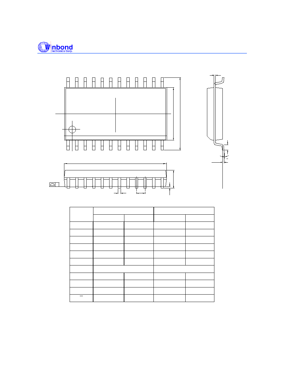
12. PACKAGE DRAWING AND DIMENSIONS
12.1. 20L (PDIP) P
LASTIC
D
UAL
I
NLINE
P
ACKAGE
D
IMENSIONS
(W682510
ONLY
)
Seating
A
e
2
A
1
1
1
2
B
B
1
D
1
E
S
A
e
1
1
A
Base
E
c
·
L
DIMENSION (MM)
DIMENSION (INCH)
SYMBOL
MIN. NOM. MAX. MIN. NOM. MAX.
A - - 4.45 - - 0.175
A
1
0.25 -
- 0.010 -
-
A
2
3918
3.30 3.43
0.125 0.130 0.135
B 0.41
0.46
0.56
0.016 0.018 0.022
B
1
1.47
1.52 1.63
0.058 0.060 0.064
c 0.20
0.25
0.36
0.008 0.010 0.014
D -
20.06
26.42
-
1.026
1.046
E 7.37
7.62
7.87
0.290 0.300 0.310
E
1
6.22
6.35 6.48
0.245 0.250 0.255
e
1
2.29
2.54 2.79
0.090 0.100 0.110
L 3.05
3.30
3.56
0.120 0.130 0.140
· 0∫ - 15∫ 0∫ - 15∫
e
A
8.51
9.02 9.53
0.335 0.355 0.375
S - - 1.91 - - 0.075
Publication Release Date: May 2003
- 31 -
Revision 0.35
W682510/W682310
- 32 -
12.2. 20L SSOP ≠ 209
MIL
S
HRINK
S
MALL
O
UTLINE
P
ACKAGE
D
IMENSIONS
D
1
2
DTEAIL
E
H E
1
1
DIMENSION (MM)
DIMENSION (INCH)
SYMBOL
MIN. NOM. MAX. MIN. NOM. MAX.
A - - 2.00
- - 0.079
A1 0.05 -
- 0.002 -
-
A2 1.65 1.75 1.85
0.065
0.069 -
b 0.22 - 0.38
0.009 - 0.015
c 0.09 - 0.25
0.004 - 0.010
D 6.90
7.20 7.50
0.272 0.283 0.295
E 5.00
5.30 5.60
0.197 0.209 0.220
H
E
7.40 7.80 8.20 0.291 0.307 0.323
e -
0.65 - -
0.0256
-
L 0.55
0.75 0.95
0.021 0.030 0.037
L1 -
1.25 - -
0.050 -
Y - - 0.10
- - 0.004
0 0∫ - 8∫ 0 - 8∫
e
Y
b
A
A A
SEATING
L
L
DETAIL
SEATING
b
W682510/W682310
12.3. 24 SOP ≠ 300
MIL
L
O
c
E
H
A1
A
e
b
D
SEATI
NG PLANE
Y
0.25
GAUGE PLANE
DIMENSION (MM)
DIMENSION (INCH)
SYMBOL
MIN. MAX. MIN. MAX.
A 2.35 2.65 0.093 0.104
A1 0.10 0.30 0.004 0.012
b 0.33 0.51 0.013 0.020
c 0.23 0.32 0.009 0.013
E 7.40 7.60 0.291 0.299
D 15.20 15.60 0.598 0.614
e
1.27 BSC
0.050 BSC
H
E
10.00 10.65 0.394 0.419
Y 0.10 0.004
L 0.10 1.27 0.016 0.050
0 0∫ 8∫ 0 8∫
Publication Release Date: May 2003
- 33 -
Revision 0.35

W682510/W682310
13. ORDERING INFORMATION
Product Number Descriptor Key
Product Family
W682510 Product
W682510 _
Package Type:
E
=
20-Lead Plastic Dual Inline Package (PDIP)
S
=
24-Lead Plastic Small Outline Package (SOP)
R
=
20-Lead Plastic Small Outline Package (SSOP)
When ordering W682510 series devices, please refer to the following part numbers.
Part Number
W682510E
W682510S
W682510R
Product Family
W682310 Product
W682310 _
Package Type:
S
=
24-Lead Plastic Small Outline Package (SOP)
R
=
20-Lead Plastic Small Outline Package (SSOP)
When ordering W682310 series devices, please refer to the following part numbers.
Part Number
W682310S
W682310R
For the latest product information, access Winbond's worldwide website at
HTTP://WWW.WINBOND-USA.COM
- 34 -
W682510/W682310
14. VERSION HISTORY
VERSION
DATE
PAGE
DESCRIPTION
0.31
Mar 2003
All
Preliminary Specifications
0.34 Apr.
2003 Updates
0.35
May 2003
Frequency response updated
Publ
Headquarters
Winbond Electronics Corporation America Winbond Electronics (Shanghai) Ltd.
No. 4, Creation Rd. III
2727 North First Street, San Jose,
27F, 299 Yan An W. Rd. Shanghai,
Science-Based Industrial Park, CA 95134, U.S.A.
200336 China
Hsinchu, Taiwan
TEL: 1-408-9436666
TEL: 86-21-62365999
TEL: 886-3-5770066
FAX: 1-408-5441797
FAX: 86-21-62356998
FAX: 886-3-5665577
http://www.winbond-usa.com/
http://www.winbond.com.tw/
Taipei Office
Winbond Electronics Corporation Japan Winbond Electronics (H.K.) Ltd.
9F, No. 480, Pueiguang Rd. 7F Daini-ueno BLDG. 3-7-18
Unit 9-15, 22F, Millennium City,
Neihu District
Shinyokohama Kohokuku,
No. 378 Kwun Tong Rd.,
Taipei, 114 Taiwan
Yokohama, 222-0033
Kowloon, Hong Kong
TEL: 886-2-81777168
TEL: 81-45-4781881
TEL: 852-27513100
FAX: 886-2-87153579
FAX: 81-45-4781800
FAX: 852-27552064
Please note that all data and specifications are subject to change without notice.
All the trademarks of products and companies mentioned in this datasheet belong to their respective owners.
This product incorporates SuperFlashÆ technology licensed From SST.
ication Release Date: May 2003
- 35 -
Revision 0.35