 | –≠–ª–µ–∫—Ç—Ä–æ–Ω–Ω—ã–π –∫–æ–º–ø–æ–Ω–µ–Ω—Ç: W78IE52 | –°–∫–∞—á–∞—Ç—å:  PDF PDF  ZIP ZIP |

Preliminary W78IE52
8-BIT MICROCONTROLLER
Publication Release Date: April 20, 2005
- 1 -
Revision A2
1. GENERAL DESCRIPTION
The W78IE52 is an 8-bit microcontroller which can accommodate a wider frequency range with low
power consumption. The instruction set for the W78IE52 is fully compatible with the standard 8051.
The W78IE52 contains an 8K bytes Flash EPROM; a 256 bytes RAM; four 8-bit bi-directional and bit-
addressable I/O ports; an additional 4-bit I/O port P4; three 16-bit timer/counters; a hardware
watchdog timer and a serial port. These peripherals are supported by eight sources two-level interrupt
capability. To facilitate programming and verification, the Flash EPROM inside the W78IE52 allows the
program memory to be programmed and read electronically. Once the code is confirmed, the user can
protect the code for security.
The W78IE52 microcontroller has two power reduction modes, idle mode and power-down mode, both
of which are software selectable. The idle mode turns off the processor clock but allows for continued
peripheral operation. The power-down mode stops the crystal oscillator for minimum power
consumption. The external clock can be stopped at any time and in any state without affecting the
processor.
2. FEATURES
∑
Fully static design 8-bit CMOS microcontroller
∑
Wide supply voltage of 2.4V to 5.5V
∑
Industrial temperature grade -40∫C
-
85∫C
∑
256 bytes of on-chip scratchpad RAM
∑
8 KB electrically erasable/programmable Flash EPROM
∑
64 KB program memory address space
∑
64 KB data memory address space
∑
Four 8-bit bi-directional ports
∑
One extra 4-bit bit-addressable I/O port, additional INT2 / INT3
(available on 44-pin PLCC package)
∑
Three 16-bit timer/counters
∑
One full duplex serial port (UART)
∑
Watchdog Timer
∑
Eight sources, two-level interrupt capability
∑
EMI reduction mode
∑
Built-in power management
∑
Code protection mechanism
∑
Packages:
-
DIP 40: W78IE52
-
PLCC 44: W78IE52P
Comment [W1]:
Preliminary W78IE52
- 2 -
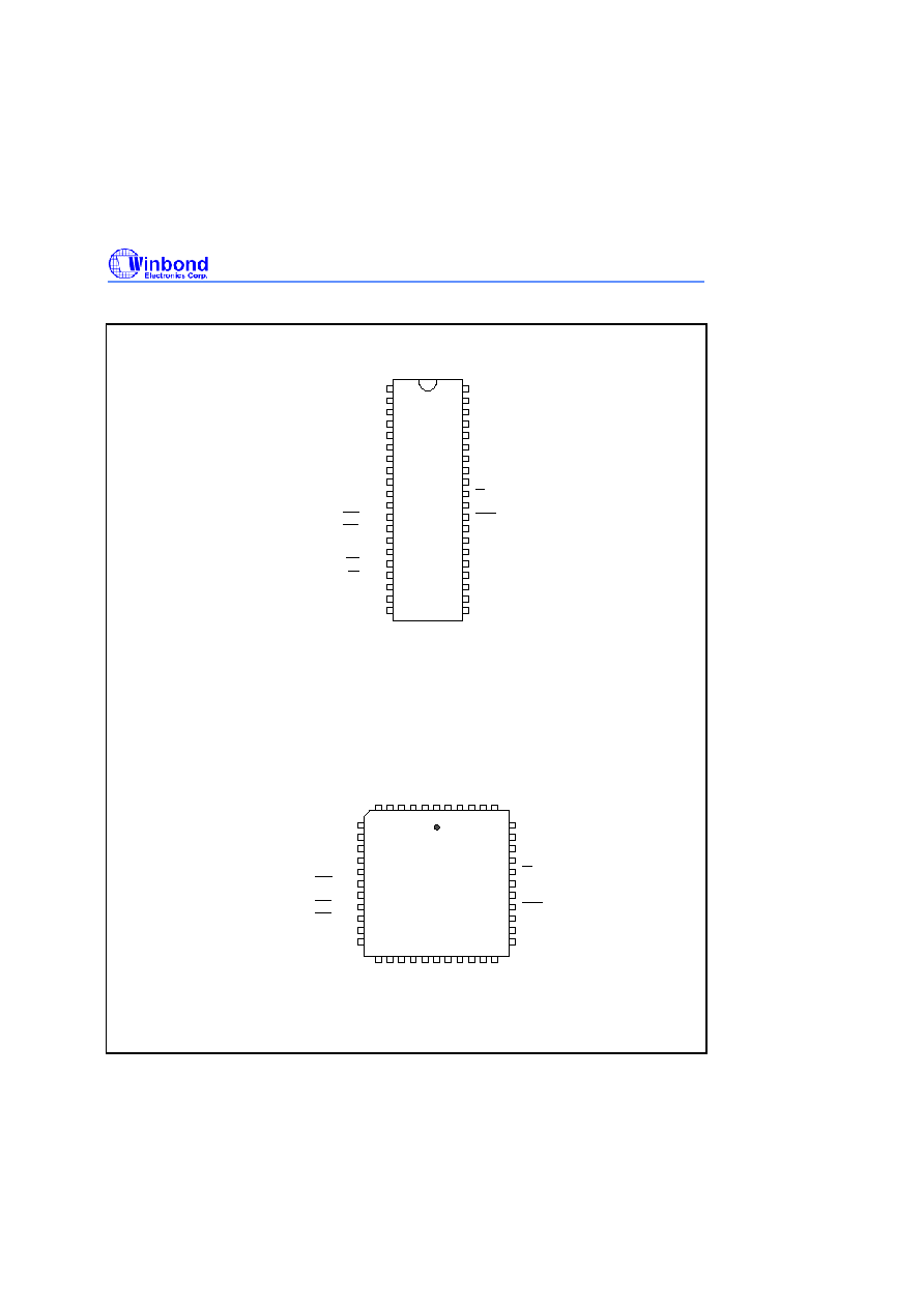
3. PIN CONFIGURATIONS
VDD
1
2
3
4
5
6
7
8
9
10
11
12
13
14
15
16
17
18
19
20
39
40
34
35
36
37
38
30
31
32
33
26
27
28
29
21
22
23
24
25
P0.0, AD0
P0.1, AD1
P0.2, AD2
P0.3, AD3
P0.4, AD4
P0.5, AD5
P0.6, AD6
P0.7, AD7
EA
ALE
PSEN
P2.5, A13
P2.6, A14
P2.7, A15
P2.0, A8
P2.1, A9
P2.2, A10
P2.3, A11
P2.4, A12
T2, P1.0
40-Pin DIP (W78IE52)
P1.2
P1.3
P1.4
P1.5
P1.6
RXD, P3.0
TXD, P3.1
P1.7
RST
INT0, P3.2
INT1, P3.3
T0, P3.4
T1, P3.5
WR, P3.6
RD, P3.7
XTAL1
XTAL2
VSS
T2EX, P1.1
44-Pin PLCC (W78IE52P)
40
2 1 44 43 42 41
6 5 4 3
39
38
37
36
35
34
33
32
31
30
29
P0.4, AD4
P0.5, AD5
P0.6, AD6
P0.7, AD7
EA
ALE
PSEN
P2.7, A15
P2.6, A14
P2.5, A13
28
27
26
25
24
23
22
21
20
19
18
17
10
9
8
7
14
13
12
11
16
15
P1.5
P1.6
P1.7
RST
RXD, P3.0
TXD, P3.1
INT0, P3.2
INT1, P3.3
T0, P3.4
T1, P3.5
A
D
3
,
P
0
.
3
T
2
,
P
1
.
0
P
1
.
2
V
D
D
A
D
2
,
P
0
.
2
A
D
1
,
P
0
.
1
A
D
0
,
P
0
.
0
T
2
E
X
,
P
1
.
1
P
1
.
3
P
1
.
4
X
T
A
L
1
V
S
S
P
2
.
4
,
A
1
2
P
2
.
3
,
A
1
1
P
2
.
2
,
A
1
0
P
2
.
1
,
A
9
P
2
.
0
,
A
8
X
T
A
L
2
P
3
.
7
,
/
R
D
P
3
.
6
,
/
W
R
P4.1
P
4
.
0
INT2, P4.3
/
I
N
T
3
,
P
4
.
2

Preliminary W78IE52
Publication Release Date: April 20, 2005
- 3 -
Revision A2
4. PIN DESCRIPTION
SYMBOL DESCRIPTIONS
EA
EXTERNAL ACCESS ENABLE: This pin forces the processor to execute out of
external ROM. It should be kept high to access internal ROM. The ROM address and
data will not be presented on the bus if EA pin is high and the program counter is
within on-chip ROM area.
PSEN
PROGRAM STORE ENABLE: PSEN enables the external ROM data onto the Port 0
address/ data bus during fetch and MOVC operations. When internal ROM access is
performed, no PSEN strobe signal outputs from this pin.
ALE
ADDRESS LATCH ENABLE: ALE is used to enable the address latch that separates
the address from the data on Port 0.
RST
RESET: A high on this pin for two machine cycles while the oscillator is running resets
the device.
XTAL1
CRYSTAL1: This is the crystal oscillator input. This pin may be driven by an external
clock.
XTAL2
CRYSTAL2: This is the crystal oscillator output. It is the inversion of XTAL1.
V
SS
GROUND: Ground potential
V
DD
POWER SUPPLY: Supply voltage for operation.
P0.0
-
P0.7 PORT 0: Port 0 is a bi-directional I/O port which also provides a multiplexed low order
address/data bus during accesses to external memory. The Port 0 is also an open-drain
port and external pull-ups need to be connected while in programming.
P1.0
-
P1.7 PORT 1: Port 1 is a bi-directional I/O port with internal pull-ups. The bits have alternate
functions which are described below:
T2(P1.0): Timer/Counter 2 external count input
T2EX(P1.1): Timer/Counter 2 Reload/Capture control
P2.0
-
P2.7 PORT 2: Port 2 is a bi-directional I/O port with internal pull-ups. This port also provides
the upper address bits for accesses to external memory.
P3.0
-
P3.7 PORT 3: Port 3 is a bi-directional I/O port with internal pull-ups. All bits have alternate
functions, which are described below:
RXD(P3.0) : Serial Port receiver input
TXD(P3.1) : Serial Port transmitter output
INT0 (P3.2): External Interrupt 0
INT1(P3.3): External Interrupt 1
T0(P3.4) : Timer 0 External Input
T1(P3.5) : Timer 1 External Input
WR
(P3.6) : External Data Memory Write Strobe
RD (P3.7) : External Data Memory Read Strobe
P4.0
-
P4.3 PORT 4: Another bit-addressable bidirectional I/O port P4. P4.3 and P4.2 are alternative
function pins. It can be used as general I/O port or external interrupt input sources
(INT2 /INT3 ).
Preliminary W78IE52
- 4 -
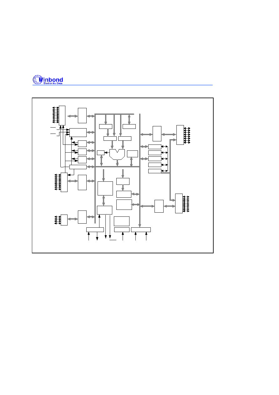
5. BLOCK DIAGRAM
P3.0
~
P3.7
P1.0
~
P1.7
ALU
Port 0
Latch
Port 1
Latch
Timer
1
Timer
0
Timer
2
Port
1
UART
XTAL1
PSEN
ALE
Vss
Vcc
RST
XTAL2
Oscillator
Interrupt
PSW
Instruction
Decoder
&
Sequencer
Reset Block
Bus & Clock
Controller
SFR RAM
Address
Power control
256 bytes
RAM & SFR
Stack
Pointer
B
Addr. Reg.
Incrementor
PC
DPTR
Temp Reg.
T2
T1
ACC
Port 3
Latch
Port 4
Latch
Port
3
Port 2
Latch
P4.0
~
P4.3
Port
4
Port
0
Port
2
P2.0
~
P2.7
P0.0
~
P0.7
INT2
INT3
Watchdog
Timer
ROM
6. FUNCTIONAL DESCRIPTION
The W78IE52 architecture consists of a core controller surrounded by various registers, five general
purpose I/O ports, 256 bytes of RAM, three timer/counters, and a serial port. The processor supports
111 different opcodes and references both a 64K program address space and a 64K data storage
space.
Timers 0, 1, and 2
Timers 0, 1, and 2 each consist of two 8-bit data registers. These are called TL0 and TH0 for Timer 0,
TL1 and TH1 for Timer 1, and TL2 and TH2 for Timer 2. The TCON and TMOD registers provide
control functions for timers 0 and 1. The T2CON register provides control functions for Timer 2.
RCAP2H and RCAP2L are used as reload/capture registers for Timer 2.
Preliminary W78IE52
Publication Release Date: April 20, 2005
- 5 -
Revision A2
The operations of Timer 0 and Timer 1 are the same as in the W78C51. Timer 2 is a special feature of
the W78IE52: it is a 16-bit timer/counter that is configured and controlled by the T2CON register. Like
Timers 0 and 1, Timer 2 can operate as either an external event counter or as an internal timer,
depending on the setting of bit C/T2 in T2CON. Timer 2 has three operating modes: capture, auto-
reload, and baud rate generator. The clock speed at capture or auto-reload mode is the same as that
of Timers 0 and 1.
New Defined Peripheral
In order to be more suitable for I/O, an extra 4-bit bit-addressable port P4 and two external interrupt
INT2 , INT3 has been added to either the PLCC or QFP 44 pin package. And description follows:
1.
INT2
/
INT3
Two additional external interrupts, INT2 and INT3 , whose functions are similar to those of external
interrupt 0 and 1 in the standard 80C52. The functions/status of these interrupts are
determined/shown by the bits in the XICON (External Interrupt Control) register. The XICON register is
bit-addressable but is not a standard register in the standard 80C52. Its address is at 0C0H. To
set/clear bits in the XICON register, one can use the "SETB (/CLR) bit" instruction. For example,
"SETB 0C2H" sets the EX2 bit of XICON.
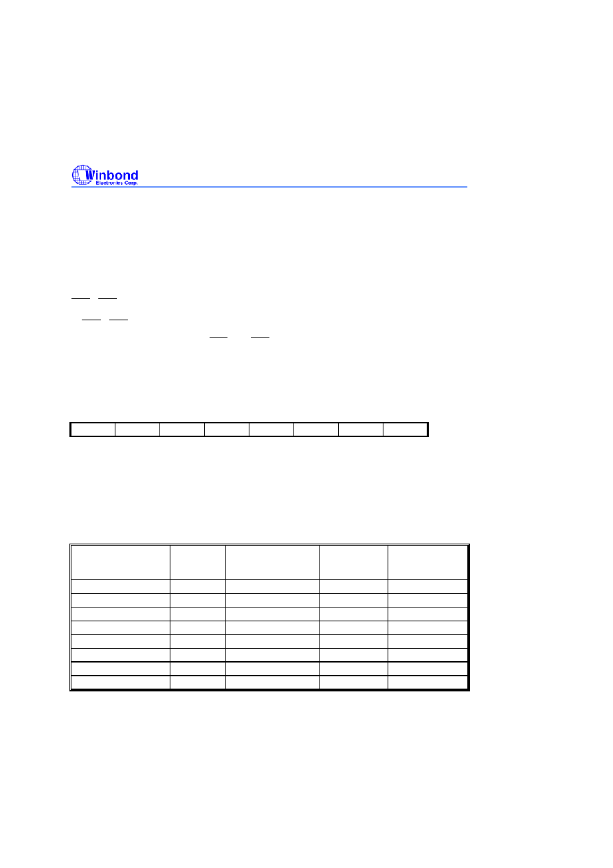
XICON - external interrupt control (C0H)
PX3 EX3 IE3 IT3 PX2 EX2 IE2 IT2
PX3: External interrupt 3 priority high if set
EX3: External interrupt 3 enable if set
IE3: If IT3 = 1, IE3 is set/cleared automatically by hardware when interrupt is detected/serviced
IT3: External interrupt 3 is falling-edge/low-level triggered when this bit is set/cleared by software
PX2: External interrupt 2 priority high if set
EX2: External interrupt 2 enable if set
IE2: If IT2 = 1, IE2 is set/cleared automatically by hardware when interrupt is detected/serviced
IT2: External interrupt 2 is falling-edge/low-level triggered when this bit is set/cleared by software
INTERRUPT SOURCE
VECTOR
ADDRESS
POLLING
SEQUENCE WITHIN
PRIORITY LEVEL
ENABLE
REQUIRED
SETTINGS
INTERRUPT
TYPE
EDGE/LEVEL
External Interrupt 0
03H
0 (highest)
IE.0
TCON.0
Timer/Counter 0
0BH
1
IE.1
-
External Interrupt 1
13H
2
IE.2
TCON.2
Timer/Counter 1
1BH
3
IE.3
-
Serial Port
23H
4
IE.4
-
Timer/Counter 2
2BH
5
IE.5
-
External Interrupt 2
33H
6
XICON.2
XICON.0
External Interrupt 3
3BH
7 (lowest)
XICON.6
XICON.3