
W83194AR-96
200MHZ CLOCK FOR WHITNEY CHIPSET
Publication Release Date: June 1999
W83194AR-96
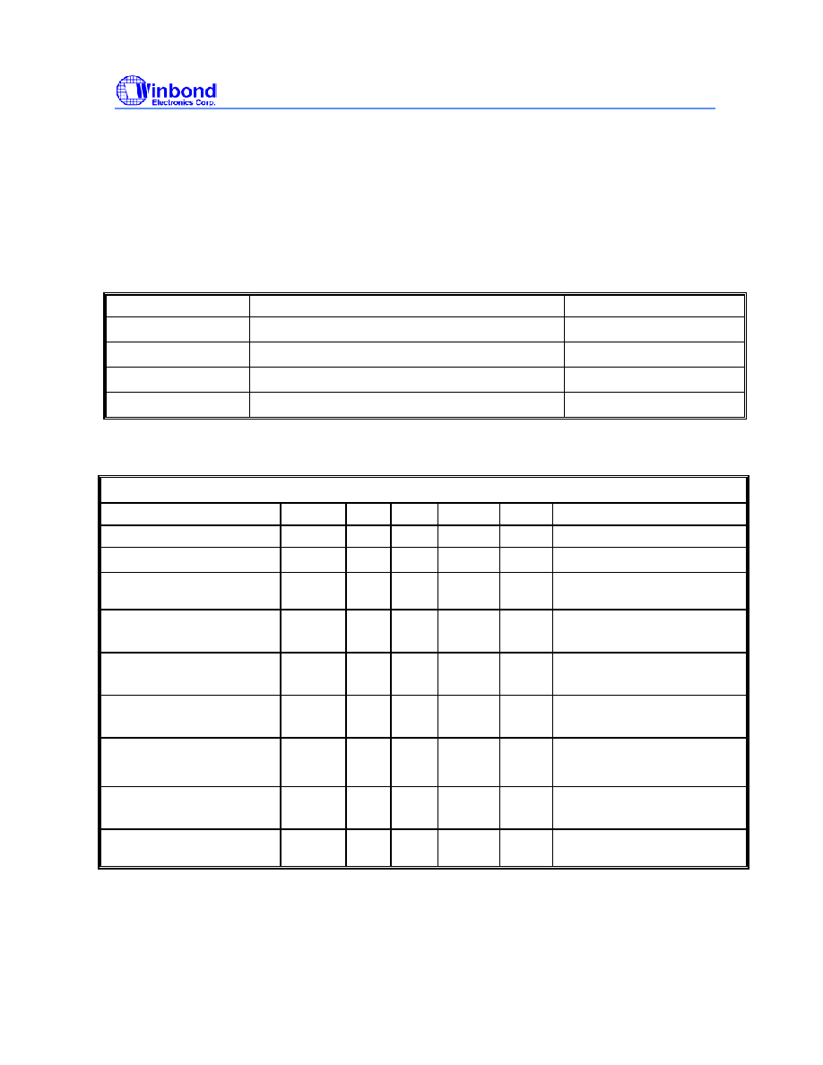
Data Sheet Revision History
Pages Dates Version Version
On Web
Main Contents
1
n.a.
n.a.
All of the versions before 0.50 are for internal use.
2
n.a.
02/Apr
1.0
1.0
Change version and version on web site to 1.0
3
4
5
6
7
8
9
10
Please note that all data and specifications are subject to change without notice. All the trademarks of
products and companies mentioned in this data sheet belong to their respective owners.
LIFE SUPPORT APPLICATIONS
These products are not designed for use in life support appliances, devices, or systems where
malfunction of these products can reasonably be expected to result in personal injury. Winbond
customers using or selling these products for use in such applications do so at their own risk and
agree to fully indemnify Winbond for any damages resulting from such improper use or sales.
- 1 - Revision 1.0

W83194AR-96
Publication Release Date: June 1999
1.0 GENERAL DESCRIPTION
The W83194AR-96 is a Clock Synthesizer for Intel Whitney chipset. W83194AR-96 provides all
clocks required for high-speed RISC or CISC microprocessor and also provides 32 different
frequencies of CPU, SDRAM, PCI, 3V66, IOAPIC clocks frequency setting. All clocks are externally
selectable with smooth transitions.
The W83194AR-96 provides I
2
C serial bus interface to program the registers to enable or disable
each clock outputs and provides 0.25% center and 0-0.5% down type spread spectrum to reduce EMI.
The W83194AR-96 accepts a 14.318 MHz reference crystal as its input and runs on a 3.3V supply.
High drive PCI and SDRAM CLOCK outputs typically provide greater than 1 V /ns slew rate into 30 pF
loads. CPU CLOCK outputs typically provide better than 1 V /ns slew rate into 20 pF loads as
maintaining 50� 5% duty cycle. The fixed frequency outputs as REF, 24MHz, and 48 MHz provide
better than 0.5V /ns slew rate.
1.0 PRODUCT FEATURES
� 2 CPU clocks
� 9 SDRAM clocks for 2 DIMMs
� 8 PCI synchronous clocks.
� Optional single or mixed supply:
(VDDR = VDDP=VDDS = VDD48 = VDD3 = 3.3V, VDDA=VDDC=2.5V)
� Skew form CPU to PCI clock -1 to 4 ns, center 2.6 ns
� Smooth frequency switch with selections from 66.8 to 200MHz
� I
2
C 2-Wire serial interface and I
2
C read back
� 0.25% or 0.5% center type spread spectrum
� Programmable registers to enable/stop each output and select modes
(mode as Tri-state or Normal )
� 48 MHz for USB
� 24 MHz for super I/O
� Packaged in 48-pin SSOP
- 2 - Revision 1.0
W83194AR-96
Publication Release Date: June 1999
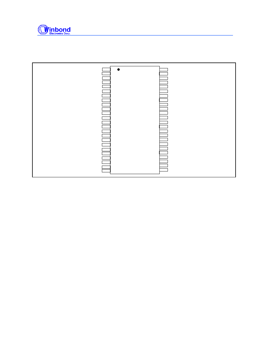
3.0 PIN CONFIGURATION
48
47
46
45
44
43
42
41
40
39
38
37
36
35
34
33
32
31
30
29
28
27
26
25
1
2
3
4
5
6
7
8
9
10
11
12
13
14
15
16
17
18
19
20
21
22
23
24
VDDR
VSS
Xin
Xout
VDD3
PCICLK0/ FS0#
VSS
PCICLK6
PCICLK2/*SEL24_48#
PCICLK3/ FS4#
PCICLK4
SDRAM_F
VSS
3V66-0
VDDP
PD#
*SDATA
*SDCLK
VddA
IOAPIC
VSS
REF1/*APIC_SEL
CPUCLK0
VDDC
CPUCLK1
VSS
SDRAM 0
SDRAM 1
SDRAM 2
VDDS
SDRAM 3
VSS
SDRAM 4
SDRAM 5
SDRAM 6
SDRAM 7
VSS
VDDS
48MHz-1/ FS3#
24_48MHz/ FS2#
PCICLK5
VDD48
VSS
3V66-1
VDDP
PCICLK1/ FS1#
PCICLK7
48MHz-0
- 3 - Revision 1.0
W83194AR-96
Publication Release Date: June 1999
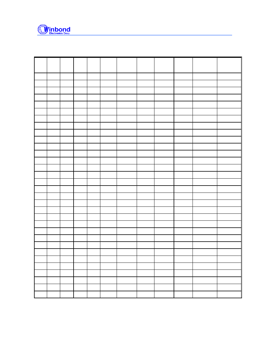
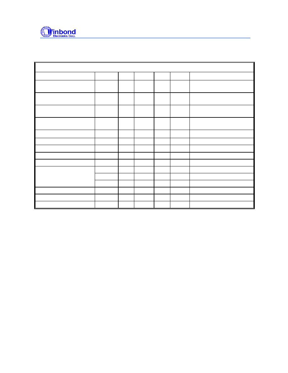
4.0 FREQUENCY SELECTION BY HARDWARE
FS4 FS3 FS2 FS1 FS0 CPU
(MHz)
SDRAM
(MHz)
CPU
/SDRAM
3V66
(MHz)
PCI(MHz) IOAPIC (MHz)
APIC_SEL=1
IOAPIC (MHz)
APIC_SEL=0
0 0 0 0 0
66.8 100.2 2/3
66.80
33.40
16.70
33.40
0
0
0
0
1
90
90
1
60.00
30.00
15.00
30.00
0 0 0 1 0
100.2 100.2 1
66.80
33.40
16.70
33.40
0 0 0 1 1 72 108 2/3 72.00
36.00
18.00
36.00
0 0 1 0 0
133.6 133.6 1
66.80
33.40
16.70
33.40
0 0 1 0 1
95.25
95.25 1 63.50
31.75
15.88
31.75
0 0 1 1 0
133.6 100.2 4/3
66.80
33.40
16.70
33.40
0
0
1
1
1
124
124
1
82.67
41.33
20.67
41.33
0
1
0
0
0
119
119
1
79.33
39.67
19.83
39.67
0
1
0
0
1
114
114
1
76.00
38.00
19.00
38.00
0
1
0
1
0
110
110
1
73.33
36.67
18.33
36.67
0
1
0
1
1
105
105
1
70.00
35.00
17.50
35.00
0 1 1 0 0
83.3 124.95 2/3
83.30
41.65
20.83
41.65
0 1 1 0 1
75 112.5 2/3
75.00
37.50
18.75
37.50
0 1 1 1 0
89.07 133.6 2/3 89.07
44.53
22.27
44.53
0 1 1 1 1
121
121
1
80.67
40.33
20.17
40.33
1 0 0 0 0 135 101.25 4/3 67.50
33.75
16.88
33.75
1
0
0
0
1
125
125
1
83.33
41.67
20.83
41.67
1
0
0
1
0
127
127
1
84.67
42.33
21.17
42.33
1
0
0
1
1
130
130
1
86.67
43.33
21.67
43.33
1
0
1
0
0
140
140
1
70.00
35.00
17.50
35.00
1
0
1
0
1
136
136
1
68.00
34.00
17.00
34.00
1
0
1
1
0
166
166
1
83.00
41.50
20.75
41.50
1
0
1
1
1
155
155
1
77.50
38.75
19.38
38.75
1 1 0 0 0
150 112.5 4/3 75.00
37.50
18.75
37.50
1
1
0
0
1
117
117
1
78.00
39.00
19.50
39.00
1
1
0
1
0
107
107
1
71.33
35.67
17.83
35.67
1 1 0 1 1
100.9
100.9 1 67.27
33.63
16.82
33.63
1 1 1 0 0
145 108.75 4/3 72.50
36.25
18.13
36.25
1 1 1 0 1
140 105 4/3 70.00
35.00
17.50
35.00
1 1 1 1 0
138 103.5 4/3 69.00
34.50
17.25
34.50
1 1 1 1 1
137 102.75 4/3 68.50
34.25
17.13
34.25
- 4 - Revision 1.0

W83194AR-96
Publication Release Date: June 1999
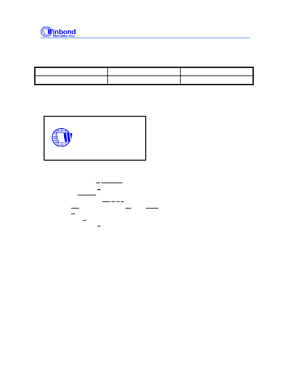
5.0
SERIAL CONTROL 0REGISTERS
The Pin column lists the affected pin number and the @PowerUp column gives the state at true power
up. Registers are set to the values shown only on true power up. "Command Code" byte and "Byte
Count" byte must be sent following the acknowledge of the Address Byte. Although the data (bits)
in these two bytes are considered "don't care", they must be sent and will be acknowledge. After
that, the below described sequence (Register 0, Register 1, Register 2, ....) will be valid and
acknowledged.
Frequency Table Setting by I2C (SEL5 ~ SEL0)
SS
EL5
SS
EL4
SS
EL3
SS
EL2
SS
EL1
SS
EL0
CPU
(MHz)
SDRAM
(MHz)
CPU/SD
RAM
3V66
(MHz)
PCI
(MHz)
IOAPIC (MHz)
APIC_SEL=1
IOAPIC (MHz)
APIC_SEL=0
0 0 0 0 0 0
66.8 100.2 2/3
66.80
33.40
16.70
33.40
0
0
0
0
0
1
90
90
1
60.00
30.00
15.00
30.00
0 0 0 0 1 0
100.2 100.2
1
66.80
33.40
16.70
33.40
0 0 0 0 1 1 72 108 2/3 72.00
36.00
18.00
36.00
0 0 0 1 0 0
133.6 133.6
1
66.80
33.40
16.70
33.40
0 0 0 1 0 1 95.25
95.25 1 63.50
31.75
15.88
31.75
0 0 0 1 1 0
133.6 100.2 4/3
66.80
33.40
16.70
33.40
0
0
0
1
1
1
124
124
1
82.67
41.33
20.67
41.33
0
0
1
0
0
0
119
119
1
79.33
39.67
19.83
39.67
0
0
1
0
0
1
114
114
1
76.00
38.00
19.00
38.00
0
0
1
0
1
0
110
110
1
73.33
36.67
18.33
36.67
0
0
1
0
1
1
105
105
1
70.00
35.00
17.50
35.00
0 0 1 1 0 0 83.3
124.95 2/3
83.30
41.65
20.83
41.65
0 0 1 1 0 1 75 112.5 2/3
75.00
37.50
18.75
37.50
0 0 1 1 1 0 89.07
133.6 2/3 89.07
44.53
22.27
44.53
0
0
1
1
1
1
121
121
1
80.67
40.33
20.17
40.33
0 1 0 0 0 0 135 101.25 4/3 67.50 33.75
16.88
33.75
0
1
0
0
0
1
125
125
1
83.33
41.67
20.83
41.67
0
1
0
0
1
0
127
127
1
84.67
42.33
21.17
42.33
0
1
0
0
1
1
130
130
1
86.67
43.33
21.67
43.33
0
1
0
1
0
0
140
140
1
70.00
35.00
17.50
35.00
0
1
0
1
0
1
136
136
1
68.00
34.00
17.00
34.00
0
1
0
1
1
0
166
166
1
83.00
41.50
20.75
41.50
0
1
0
1
1
1
155
155
1
77.50
38.75
19.38
38.75
0 1 1 0 0 0
150 112.5 4/3 75.00 37.50
18.75
37.50
0
1
1
0
0
1
117
117
1
78.00
39.00
19.50
39.00
0
1
1
0
1
0
107
107
1
71.33
35.67
17.83
35.67
0 1 1 0 1 1 100.9
100.9 1 67.27
33.63
16.82
33.63
0 1 1 1 0 0
145 108.75 4/3 72.50 36.25
18.13
36.25
0 1 1 1 0 1
140 105 4/3 70.00
35.00
17.50
35.00
0 1 1 1 1 0
138 103.5 4/3 69.00 34.50
17.25
34.50
0 1 1 1 1 1
137 102.75 4/3 68.50 34.25
17.13
34.25
- 5 - Revision 1.0
W83194AR-96
Publication Release Date: June 1999
SS
EL5
SS
EL4
SS
EL3
SS
EL2
SS
EL1
SS
EL0
CPU
(MHz)
SDRAM
(MHz)
CPU/SD
RAM
3V66
(MHz)
PCI
(MHz)
IOAPIC (MHz)
APIC_SEL=1
IOAPIC (MHz)
APIC_SEL=0
1 0 0 0 0 0 136 102.00 4/3 68.00
34.00
17.00
34.00
1 0 0 0 0 1 138 138.00 1 69.00
34.50
17.25
34.50
1 0 0 0 1 0 139 104.25 4/3 69.50
34.75
17.38
34.75
1 0 0 0 1 1 141 141.00 1 70.50
35.25
17.63
35.25
1 0 0 1 0 0 142 142.00 1 71.00 35.50
17.75
35.50
1 0 0 1 0 1 142 106.50 4/3 71.00 35.50
17.75
35.50
1 0 0 1 1 0 143 143.00 1 71.50 35.75
17.88
35.75
1 0 0 1 1 1 143 107.25 4/3 71.50 35.75
17.88
35.75
1 0 1 0 0 0 144 144.00 1 72.00
36.00
18.00
36.00
1 0 1 0 0 1 144 108.00 4/3 72.00 36.00
18.00
36.00
1
0
1
0
1
0
146
146
1
73.00
36.50
18.25
36.50
1 0 1 0 1 1 146 109.50 4/3 73.00 36.50
18.25
36.50
1 0 1 1 0 0 147 147 1
73.50
36.75
18.38
36.75
1 0 1 1 0 1 147 110.25 4/3 73.50 36.75
18.38
36.75
1 0 1 1 1 0 148 148.00 1 74.00 37.00
18.50
37.00
1 0 1 1 1 1 148 111.00 4/3 74.00 37.00
18.50
37.00
1 1 0 0 0 0 149 111.75 4/3 74.50 37.25
18.63
37.25
1 1 0 0 0 1 152 152.00 1 76.00 38.00
19.00
38.00
1 1 0 0 1 0
153 114.75 4/3 76.50 38.25
19.13
38.25
1 1 0 0 1 1 156 156.00 1 78.00 39.00
19.50
39.00
1 1 0 1 0 0
157 117.75 4/3 78.50 39.25
19.63
39.25
1 1 0 1 0 1 158 158.00 1 79.00 39.50
19.75
39.50
1 1 0 1 1 0
159 119.25 4/3 79.50 39.75
19.88
39.75
1 1 0 1 1 1 160 160.00 1 80.00 40.00
20.00
40.00
1 1 1 0 0 0
162 121.5 4/3 81.00 40.50
20.25
40.50
1 1 1 0 0 1 164 164.00 1 82.00 41.00
20.50
41.00
1 1 1 0 1 0 170 170.00 1 85.00 42.50
21.25
42.50
1 1 1 0 1 1
175
175
1
87.5
43.75
21.88
43.75
1 1 1 1 0 0
180
90
2
60
30
15
30
1 1 1 1 0 1
185 92.5
2 61.67 30.83
15.42
30.83
1 1 1 1 1 0 190 126.67 3/2 63.33 31.67
15.83
31.67
1 1 1 1 1 1 200.4 133.60 3/2 66.80 33.40
16.70
33.40
- 6 - Revision 1.0
W83194AR-96
Publication Release Date: June 1999
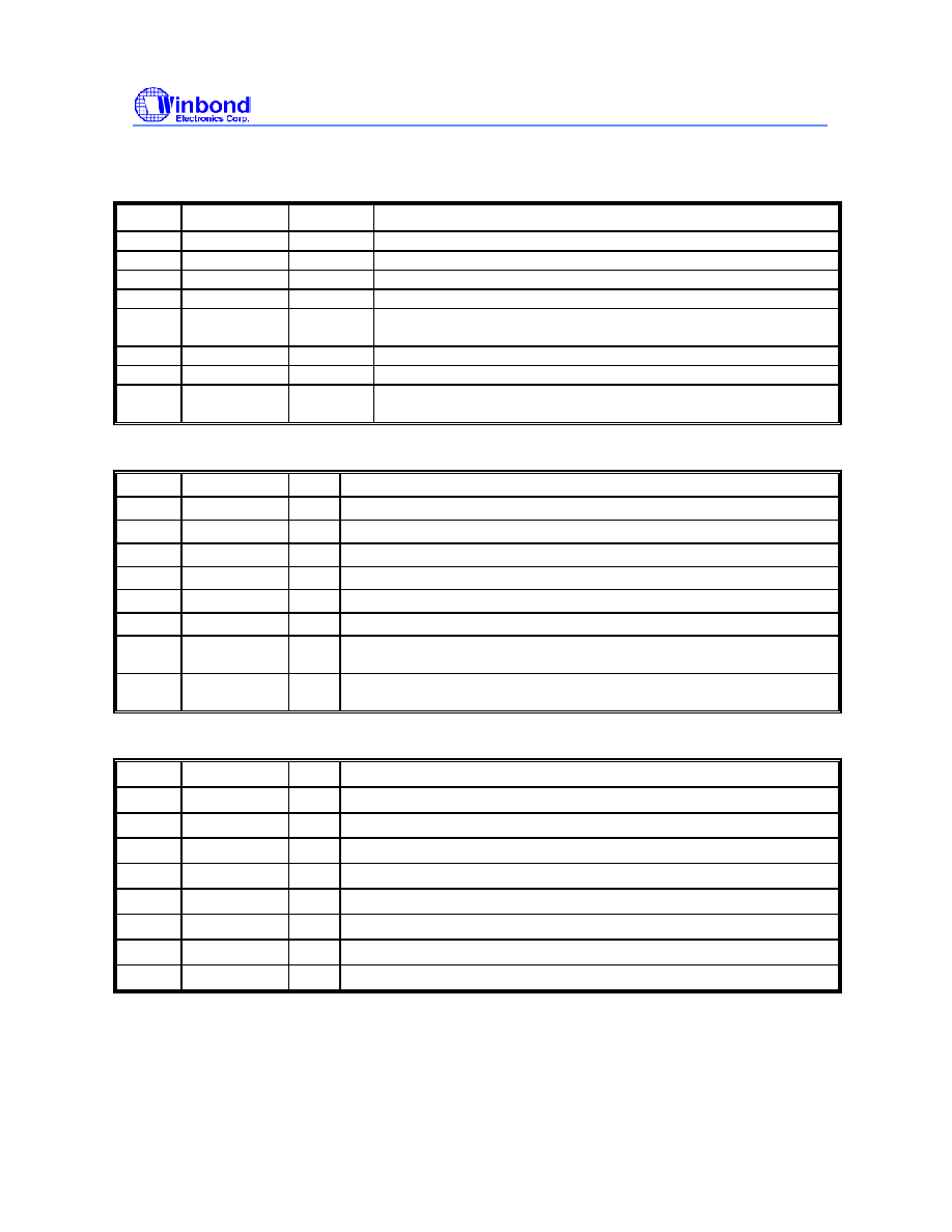
5.1 Register 0: CPU Frequency Select Register
Bit @PowerUp Pin
Description
7 0 -
SSEL3 (Frequency table selection by software via I
2
C )
6
0
-
SSEL2 ( Frequency table selection by software via I
2
C)
5
0
-
SSEL1 ( Frequency table selection by software via I
2
C)
4
0
-
SSEL0 ( Frequency table selection by software via I
2
C)
3
0
-
0 = Selection by hardware
1 = Selection by software I
2
C - Bit (2, 7:4), Register1 Bit1
2
0
-
SSEL4 (Frequency table selection by software via I
2
C )
1 0 -
SSEL5 (Frequency table selection by software via I
2
C )
0 0 -
0
= Running
1 = Tristate all outputs
5.2 Register 1 : CPU Clock Register (1 = Active, 0 = Inactive)
Bit @PowerUp
Pin
Description
7
X -
FS3#
6
X -
FS0#
5
X -
FS2#
4
1
28
24_48MHz(Active / Inactive)
3
1
27
48MHz-0(Active / Inactive)
2
1
26
48MHz-1(Active / Inactive)
1
1 -
1 = �0.25% Center type Spread Spectrum Modulation
0 =�0.5% Center type Spread Spectrum Modulation
0
0
-
0 = Normal
1 = Spread Spectrum enabled
5.3 Register 2: SDRAM Clock Register (1 = Active, 0 = Inactive)
Bit @PowerUp
Pin
Description
7
1
32
SDRAM7 (Active / Inactive)
6
1
33
SDRAM6 (Active / Inactive)
5
1
35
SDRAM5 (Active / Inactive)
4
1
36
SDRAM4 (Active / Inactive)
3
1
37
SDRAM3 (Active / Inactive)
2
1
39
SDRAM2 (Active / Inactive)
1
1
40
SDRAM1 (Active / Inactive)
0
1
41
SDRAM0 (Active / Inactive)
- 7 - Revision 1.0

W83194AR-96
Publication Release Date: June 1999
5.4 Register 3: PCI Clock Register (1 = Active, 0 = Inactive)
Bit @PowerUp
Pin
Description
7
1
20
PCICLK7 (Active / Inactive)
6
1
19
PCICLK6 (Active / Inactive)
5
1
17
PCICLK5 (Active / Inactive)
4
1
16
PCICLK4 (Active / Inactive)
3
1
15
PCICLK3 (Active / Inactive)
2
1
13
PCICLK2 (Active / Inactive)
1
1
12
PCICLK1 (Active / Inactive)
0
1
11
PCICLK0 (Active / Inactive)
5.5 Register 4: Additional Register (1 = Active, 0 = Inactive)
Bit @PowerUp
Pin
Description
7
X
- APIC_SEL#
6
1
7
3V66_0(Active / Inactive)
5 1 8
3V66_1(Active / Inactive)
4
X
-
FS4#
3 1
47
IOAPIC (Active / Inactive)
2
X
- FS1#
1
1
44
CPUCLK1(Active / Inactive)
0
1
45
CPUCLK0(Active / Inactive)
5.6 Register 5: Reserve Register
Bit @PowerUp
Pin
Description
7 1 -
Reserved
6 0 -
Reserved
5 0 -
Reserved
4
1
- SDRAM_F
3 0 -
Reserve
2 0 -
Reserve
1 0 -
Reserve
0 0 -
Reserve
- 8 - Revision 1.0

W83194AR-96
Publication Release Date: June 1999
5.7 Register 6: Winbond Chip ID Register (Read Only)
Bit @PowerUp
Pin
Description
7
1
-
Winbond Chip ID
6
0
-
Winbond Chip ID
5
0
-
Winbond Chip ID
4
1
-
Winbond Chip ID
3
1
-
Winbond Chip ID
2
0
-
Winbond Chip ID
1
0
-
Winbond Chip ID
0
0
-
Winbond Chip ID
5.8 Register 7: Winbond Chip ID Register (Read Only)
Bit @PowerUp
Pin
Description
7
0
-
Winbond Chip ID
6
0
-
Winbond Chip ID
5
1
-
Winbond Chip ID
4
0
-
Winbond Chip ID
3
0
-
Winbond Chip ID
2
0
-
Winbond Version ID
1
0
-
Winbond Version ID
0
1
-
Winbond Version ID
- 9 - Revision 1.0
W83194AR-96
Publication Release Date: June 1999
6.0 SPECIFICATIONS
6.1 ABSOLUTE MAXIMUM RATINGS
Stresses greater than those listed in this table may cause permanent damage to the device.
Precautions should be taken to avoid application of any voltage higher than the maximum rated
voltages to this circuit. Subjection to maximum conditions for extended periods may affect reliability.
Unused inputs must always be tied to an appropriate logic voltage level (Ground or Vdd).
Symbol Parameter
Rating
Vdd , V
IN
Voltage on any pin with respect to GND
- 0.5 V to + 7.0 V
T
STG
Storage Temperature
- 65
�C to + 150�C
T
B
Ambient Temperature
- 55
�C to + 125�C
T
A
Operating Temperature
0
�C to + 70�C
6.2 AC CHARACTERISTICS
VddR=Vdd3=VddP=VddS=3.3V
� 5 %, VddC = VddA= 2.375V~2.9V , T
A
= 0
�C to +70�C
Parameter Symbol
Min
Typ
Max
Units
Test
Conditions
Output Duty Cycle
45
50
55
%
Measured at 1.5V
CPU/SDRAM to PCI Offset
t
OFF
1
4
ns
15 pF Load Measured at 1.5V
Skew (CPU-CPU), (PCI-
PCI), (SDRAM-SDRAM)
t
SKEW
250
ps
15 pF Load Measured at 1.5V
CPU/SDRAM
Cycle to Cycle Jitter
t
CCJ
�250
ps
CPU/SDRAM
Absolute Jitter
t
JA
500 ps
Jitter Spectrum 20 dB
Bandwidth from Center
BW
J
500
KHz
Output Rise (0.4V ~ 2.0V)
& Fall (2.0V ~0.4V) Time
t
TLH
t
THL
0.4
1.6
ns
15 pF Load on CPU and PCI
outputs
Overshoot/Undershoot
Beyond Power Rails
V
over
0.7 1.5 V 22
at source of 8 inch
PCB run to 15 pF load
Ring Back Exclusion
V
RBE
0.7
2.1
V
Ring Back must not enter this
range.
- 10 - Revision 1.0
W83194AR-96
Publication Release Date: June 1999
6.3 DC CHARACTERISTICS
VddR=Vdd3=VddP=VddS=3.3V
� 5 %, VddC = VddA= 2.375V~2.9V , T
A
= 0
�C to +70�C
Parameter Symbol
Min
Typ
Max
Units
Test
Conditions
Input Low Voltage
V
IL
Vss-
0.3
0.8
V
dc
Input High Voltage
V
IH
2.0 Vdd
+0.3
V
dc
Input Low Current
(no pull-up Resistors)
I
IL
-5 2.0
�A
Input Low Current
(pull-up Resistors)
I
IL
-200 -100
�A
Input High Current
I
IH
-5 5
�A
Operating Current
I
DD
60
100
mA
@66M
Power Down Current
I
DDPD
400
600
�A
C
L
= 0pF
Input Frequency
Fi
14.318 MHz
Vdd=3.3V
Pin Inductance
Lpin
7
nH
Input Capacitance
C
IN
5
pF
Logic
Inputs
C
OUT
6
pF
Output pins capacitance
C
INX
13.5
22.5
pF
X1 & X2 pins
Transition Time
T
Tra
3
mS
Disable/Enable Delay
T
1
10
nS
Clock stabilization
T
STA
3 mS
- 11 - Revision 1.0
W83194AR-96
Publication Release Date: June 1999
7.0 ORDERING INFORMATION
Part Number
Package Type
Production Flow
W83194AR-96
48 PIN SSOP
Commercial, 0
�C to +70�C
8.0 HOW TO READ THE TOP MARKING
- 12 - Revision 1.0
W83194AR-96
28051234
814GAB
1st line: Winbond logo and the type number: W83194AR-96
2nd line: Tracking code 2 8051234
2: wafers manufactured in Winbond FAB 2
8051234: wafer production series lot number
3rd line: Tracking code 814 G B B
814: packages made in '98, week 14
G: assembly house ID; O means OSE, G means GR
A: Internal use code
B: IC revision
All the trade marks of products and companies mentioned in this data sheet belong to their
respective owners.
W83194AR-96
Publication Release Date: June 1999
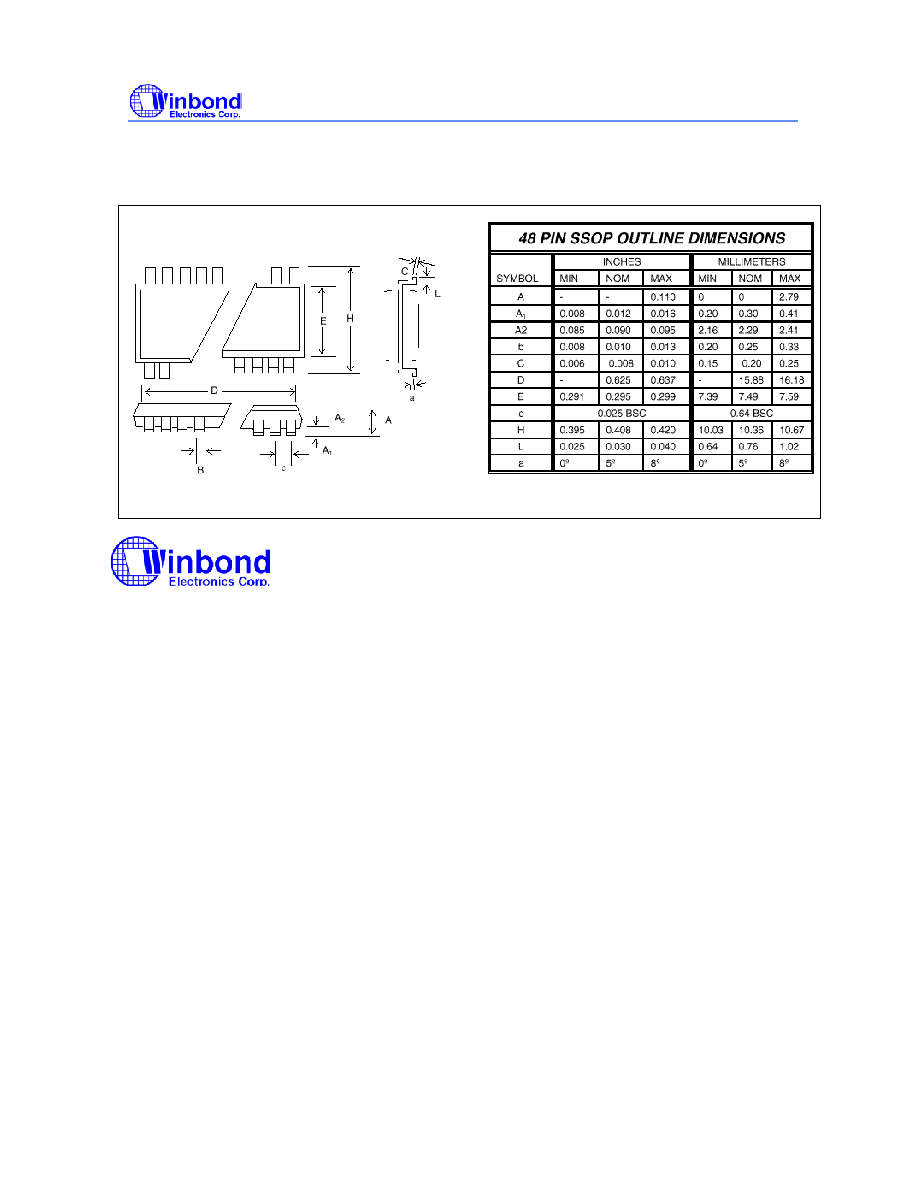
9.0 PACKAGE DRAWING AND DIMENSIONS
Headquarters
No. 4, Creation Rd. III
Science-Based Industrial Park
Hsinchu, Taiwan
TEL: 886-35-770066
FAX: 886-35-789467
www: http://www.winbond.com.tw/
Taipei Office
11F, No. 115, Sec. 3, Min-Sheng East Rd.
Taipei, Taiwan
TEL: 886-2-7190505
FAX: 886-2-7197502
TLX: 16485 WINTPE
Winbond Electronics (H.K.) Ltd.
Rm. 803, World Trade Square, Tower II
123 Hoi Bun Rd., Kwun Tong
Kowloon, Hong Kong
TEL: 852-27516023-7
FAX: 852-27552064
Winbond Electronics
(North America) Corp.
2730 Orchard Parkway
San Jose, CA 95134 U.S.A.
TEL: 1-408-9436666
FAX: 1-408-9436668
Please note that all data and specifications are subject to change without notice. All the trade
marks of products and companies mentioned in this data sheet belong to their respective
owners.
These products are not designed for use in life support appliances, devices, or systems
where malfunction of these products can reasonably be expected to result in personal injury.
Winbond customers using or selling these products for use in such applications do so at their
own risk and agree to fully indemnify Winbond for any damages resulting from such improper
use or sale.
- 13 - Revision 1.0