
W83194BR-KT
STEP-LESS 3-DIMM K7 CLOCK
Publication Release Date: June 2000
- 1 - Revision 0.43
1.0 GENERAL DESCRIPTION
The W83194BR-KT is a Clock Synthesizer which provides all clocks required for AMD K7.
W83194BR-KT provides 64 CPU/PCI frequencies which are selectable with smooth transitions by
hardware or software. W83194BR-KT also provides 13 SDRAM clocks controlled by the none-delay
buffer_in pin.
The W83194BR-KT provides step-less frequency programming by controlling the VCO freq. and the
programmable PCI clock output divisor ratio. A watchdog timer is quipped and when time out, the
RESET# pin will output 4ms pulse signal.
The W83194BR-KT accepts a 14.318 MHz reference crystal as its input. Spread spectrum built in at
±0.5% or ±0.25% to reduce EMI. Programmable stopping individual clock outputs and frequency
selection through I
2
C interface. The device meets the Pentium power-up stabilization, which requires
CPU and PCI clocks be stable within 2 ms after power-up. Using dual function pin for the slots (ISA,
PCI, CPU, DIMM) is not recommend.
2.0 PRODUCT FEATURES
∑
Supports AMD CPU with I
2
C.
∑
3 CPU clocks (one free-running chipset clock controlled by I2C)
∑
13 SDRAM clocks for 3 DIMMs
∑
6 PCI synchronous clocks
∑
Optional single or mixed supply:
(Vddq2 =2.5V, Vddq3 =3.3V)
∑
< 250ps skew among CPU and SDRAM clocks
∑
< 250ps skew among PCI clocks
∑
< 5ns propagation delay SDRAM from buffer input
∑
Skew from CPU (earlier) to PCI clock 1 to 4ns, center 2.6ns.
∑
Smooth frequency switch with selections from 66 MHz to 200 MHz CPU
∑
Step-less frequency programming by controlling the VCO freq. and the clock output divisor ratio
∑
I
2
C 2-Wire serial interface and I
2
C read back
∑
±0.25% or ±0.5% spread spectrum function to reduce EMI
∑
Programmable spread spectrum in the M/N step-less mode
∑
Programmable registers to enable/stop each output and select modes
∑
MODE pin for power Management and RESET# out when Watch Dog Timer time out
∑
One 48 MHz for USB & one 24 MHz for super I/O
∑
48-pin SSOP package
W83194BR-KT
PRELIMINARY
Publication Release Date: June 2000
- 2 - Revision 0.43
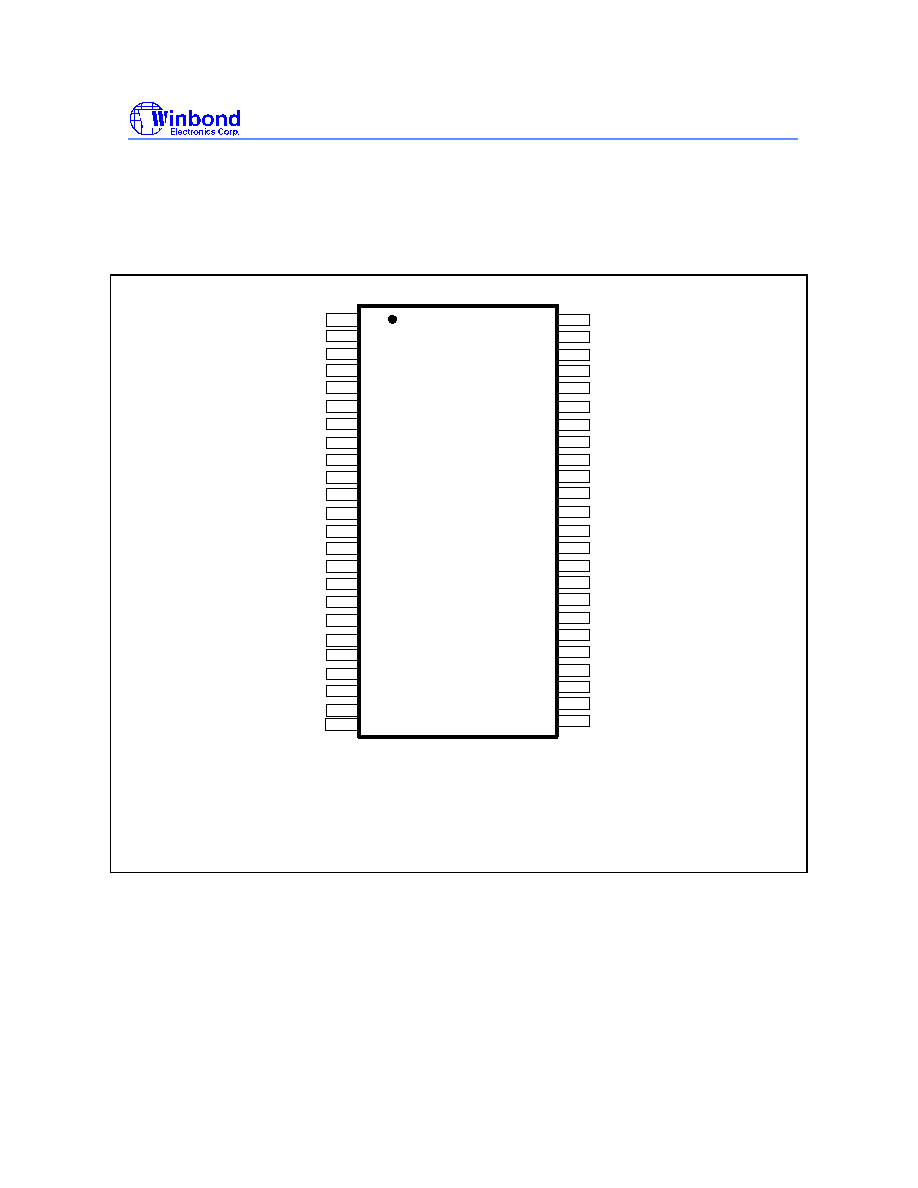
3.0 PIN CONFIGURATION
48
47
46
45
44
43
42
41
40
39
38
37
36
35
34
33
32
31
30
29
28
27
26
25
1
2
3
4
5
6
7
8
9
10
11
12
13
14
15
16
17
18
19
20
21
22
23
24
Vddq3
^ REF0/FS4*
Vss
Xin
Xout
Vddq3
PCICLK_F^/MODE1*
PCICLK1^ /FS3*
Vss
PCICLK2^/SEL24_48*
PCICLK3^
PCICLK4^
PCICLK5
Vddq3
BUFFER IN
Vss
SDRAM11
SDRAM10
Vddq3
SDRAM 9
SDRAM 8
Vss
SDATA*
SDCLK*
REF1/FS2*
Vss
CPUT_CS
CPU_C0$
Vddq2
RESET$/^PD#
SDRAM12
Vss
SDRAM 0
SDRAM 1
SDRAM 2
Vddq3
SDRAM 3
Vss
SDRAM 4
SDRAM 5
SDRAM 6
SDRAM 7
Vddq3
Vddq3
48MHz/FS0*
24_48MHz/FS1*
CPU_T0$
Vss
* : Internal pull-up
^ : 1.5X~2X driving strength
& : Internal pull-low
$ : Open Drain
# : Active Low
4.0 PIN DESCRIPTION
IN - Input
OUT - Output
I/O - Bi-directional Pin
# - Active Low
& - Internal 120k
pull-down
W83194BR-KT
PRELIMINARY
Publication Release Date: June 2000
- 3 - Revision 0.43
* - Internal 120k
pull-up
4.1 Crystal I/O
SYMBOL
PIN
I/O
FUNCTION
Xin
4
IN Crystal input with internal loading capacitors and
feedback resistors.
Xout
5
OUT Crystal output at 14.318MHz nominally.
4.2 CPU, SDRAM, PCI, IOAPIC Clock Outputs
SYMBOL
PIN
I/O
FUNCTION
CPU_C0$
CPU_T0$
43
44
OD CPU_C0 and CPU_T0 are the differential open drain
CPU clocks for AMD Athlone
TM
CPU. CPUT_CS is
the open drain pin for the chipset. It has the same
phase relationship as CPU_T0.
CPUT_CS
46
OUT CPUT_CS is the output pin for the chipset. It has the
same phase relationship as CPU_T0.
SDRAM [ 0 :12]
17,18,20,21,28,
29,31,32,34,
35,37,38,40
OUT SDRAM clock outputs. Fanout buffer outputs from
BUFFER IN pin.(Controlled by chipset) They are
disabled when PD# is set LOW.
PCICLK_F^/
*MODE1
7
I/O Free running PCI clock during normal operation.
Latched Input. Mode1=1(default), Pin 41 is RESET#
open drain. (4ms low active pulse when Watch Dog
time out), *Mode1=0, PD# input
PCICLK1^/*FS1
8
I/O Low skew (< 250ps) PCI clock outputs.
Latched input for FS1 at initial power up for H/W
selecting the output frequency of CPU, SDRAM and
PCI clocks.
PCICLK2^/SEL24_48*
10
I/O Low skew (< 250ps) PCI clock outputs.
Latched input for at initial power up for H/W
selecting the output frequency of 24_48MHz.
SEL24_48*=1(default), pin25 is 24MHz,
SEL24_48=0, pin25 is 48MHz.
PCICLK ^[ 3 : 4 ]
PCICLK 5
11,12,13
OUT Low skew (< 250ps) PCI clock outputs.
PCICLK_F and PCICLK [1:4] are double strength
pins
PCICLK 5 is not..
BUFFER IN
15
IN Inputs to fanout for SDRAM outputs.
RESET$/*PD#
41
I/O The all clocks will be stopped when this pin set to
LOW. Mode1=1(default), Pin41 is RESET$ open
drain. (4ms low active pulse when Watch Dog time
W83194BR-KT
PRELIMINARY
Publication Release Date: June 2000
- 4 - Revision 0.43
out); *Mode1=0, PD# input
4.3 I
2
C Control Interface
SYMBOL
PIN
I/O
FUNCTION
*SDATA
23
I/O Serial data of I
2
C 2-wire control interface with internal
pull-up resistor.
*SDCLK
24
IN Serial clock of I
2
C 2-wire control interface with
internal pull-up resistor.
4.4 Fixed Frequency Outputs
SYMBOL
PIN
I/O
FUNCTION
^REF0/ *FS4
2
I/O 14.318MHz reference clock.
Latched input for FS4 at initial power up for H/W
selecting the output frequency of CPU and PCI
clocks
REF1/FS2*
48
I/O 14.318MHz reference clock.
Latched input for FS2 at initial power up for H/W
selecting the output frequency of CPU and PCI
clocks.
24_48MHz / *FS1
25
I/O 24MHz output clock.
Latched input for FS1 at initial power up for H/W
selecting the output frequency of CPU and PCI
clocks.
48MHz / *FS0
26
I/O 48MHz output for USB during normal operation.
Latched input for FS0 at initial power up for H/W
selecting the output frequency of CPU and PCI
clocks.
4.5 Power Pins
SYMBOL
PIN
FUNCTION
Vddq2
42
Power supply for CPU clocks, 2.5V or 3.3V.
Vddq3
1,6,14,19,27,30,36 Power supply for PCI, 24_48MHz, SDRAM [0:12], and
CPU PLL core, nominal 3.3V.

W83194BR-KT
PRELIMINARY
Publication Release Date: June 2000
- 5 - Revision 0.43
Vss
3,9,16,22,33,39,45,
47
Circuit Ground.

W83194BR-KT
PRELIMINARY
Publication Release Date: June 2000
- 6 - Revision 0.43
5.0 FREQUENCY SELECTION
5.1 H/W Setting Frequency Table
FS4
FS3
FS2
FS1
FS0
CPU (MHz)
PCI (MHz)
0
0
0
0
0
166.00
41.60
0
0
0
0
1
160.00
40.00
0
0
0
1
0
155.00
38.70
0
0
0
1
1
150.00
37.50
0
0
1
0
0
145.00
36.20
0
0
1
0
1
140.00
35.00
0
0
1
1
0
136.00
34.00
0
0
1
1
1
130.00
32.50
0
1
0
0
0
127.00
31.70
0
1
0
0
1
124.00
31.00
0
1
0
1
0
120.00
40.00
0
1
0
1
1
118.00
39.30
0
1
1
0
0
116.00
38.60
0
1
1
0
1
115.00
38.30
0
1
1
1
0
114.00
38.00
0
1
1
1
1
113.00
37.60
1
0
0
0
0
112.00
37.30
1
0
0
0
1
111.00
37.00
1
0
0
1
0
110.00
36.60
1
0
0
1
1
109.00
36.30
1
0
1
0
0
108.00
36.00
1
0
1
0
1
107.00
35.60
1
0
1
1
0
106.00
35.30
1
0
1
1
1
104.00
34.60
1
1
0
0
0
102.00
34.00
1
1
0
0
1
133.60
33.40
1
1
0
1
0
133.90
33.40
1
1
0
1
1
133.30
33.30
1
1
1
0
0
95.00
31.70
1
1
1
0
1
100.30
33.30
1
1
1
1
0
100.90
33.40
1
1
1
1
1
100.60
33.30

W83194BR-KT
PRELIMINARY
Publication Release Date: June 2000
- 7 - Revision 0.43
6.0 MODE PIN -POWER MANAGEMENT INPUT CONTROL
MODE1, Pin7 (Latched Input)
PIN 41
1
RESET# (Open Drain)
0
PD# (Input)
7.0 FUNTION DESCRIPTION
7.1 SERIAL CONTROL REGISTERS
The Pin column lists the affected pin number and the @PowerUp column gives the default state at
true power up. "Command Code" byte and "Byte Count" byte must be sent following the
acknowledge of the Address Byte. Although the data (bits) in these two bytes are considered "don't
care", they must be sent and will be acknowledge. After that, the sequence described below
(Register 0, Register 1, Register 2, ....) will be valid and acknowledged.
Frequency table by software via I2C
SSEL4 SSEL3 SSEL2 SSEL1 SSEL0
CPU (MHz)
PCI (MHz)
0
0
0
0
0
166.00
41.60
0
0
0
0
1
160.00
40.00
0
0
0
1
0
155.00
38.70
0
0
0
1
1
150.00
37.50
0
0
1
0
0
145.00
36.20
0
0
1
0
1
140.00
35.00
0
0
1
1
0
136.00
34.00
0
0
1
1
1
130.00
32.50
0
1
0
0
0
127.00
31.70
0
1
0
0
1
124.00
31.00
0
1
0
1
0
120.00
40.00
0
1
0
1
1
118.00
39.30
0
1
1
0
0
116.00
38.60
0
1
1
0
1
115.00
38.30

W83194BR-KT
PRELIMINARY
Publication Release Date: June 2000
- 8 - Revision 0.43
0
1
1
1
0
114.00
38.00
0
1
1
1
1
113.00
37.60
SSEL4 SSEL3 SSEL2 SSEL1 SSEL0
CPU (MHz)
PCI (MHz)
1
0
0
0
0
112.00
37.30
1
0
0
0
1
111.00
37.00
1
0
0
1
0
110.00
36.60
1
0
0
1
1
109.00
36.30
1
0
1
0
0
108.00
36.00
1
0
1
0
1
107.00
35.60
1
0
1
1
0
106.00
35.30
1
0
1
1
1
104.00
34.60
1
1
0
0
0
102.00
34.00
1
1
0
0
1
133.60
33.40
1
1
0
1
0
133.90
33.40
1
1
0
1
1
133.30
33.30
1
1
1
0
0
95.00
31.70
1
1
1
0
1
100.30
33.30
1
1
1
1
0
100.90
33.40
1
1
1
1
1
100.60
33.30
7.2.1 Register 0 : Frequency Select Register (default = 0)
Bit
@PowerUp
Pin
Description
7
0
-
Reserved
6
0
-
SSEL2 (for frequency table selection by software via I
2
C)
5
0
-
SSEL1 (for frequency table selection by software via I
2
C)
4
0
-
SSEL0 (for frequency table selection by software via I
2
C)
3
0
-
0 = Selection by hardware
1 = Selection by software I
2
C - Bit 6:4, Bit2
2
0
-
SSEL4 (for frequency table selection by software via I
2
C)
1
0
-
SSEL3 (for frequency table selection by software via I
2
C)
0
0
-
0 = Running
1 = Tristate all outputs
W83194BR-KT
PRELIMINARY
Publication Release Date: June 2000
- 9 - Revision 0.43
7.2.2 Register 1 : CPU Clock Register (1 = enable, 0 = Stopped)
Bit
@PowerUp Pin
Description
7
1
-
Reserved
6
1
-
1=center type S.S.T.
0= 0-0.5% down type S.S.T.
5
0
-
0 = Normal
1 = Spread Spectrum enabled
4
0
-
0 = ±0.25% Spread Spectrum Modulation
1 = ±0.5% Spread Spectrum Modulation
3
1
-
Reserved
2
1
40 SDRAM12 (Active / Inactive)
1
1
43
44
CPUT0
CPUC0 (Active / Inactive)
0
1
46 CPUT_CS (Active / Inactive)
7.2.3 Register 2: PCI Clock Register (1 = enable, 0 = Stopped)
Bit
@PowerUp Pin
Description
7
1
-
Reserved
6
1
7
PCICLK_F (Active / Inactive)
5
1
-
Reserved
4
1
13 PCICLK5 (Active / Inactive)
3
1
12 PCICLK4 (Active / Inactive)
2
1
11 PCICLK3 (Active / Inactive)
1
1
10 PCICLK2 (Active / Inactive)
0
1
8
PCICLK1 (Active / Inactive)
7.2.4 Register 3: SDRAM, 24MHz, 48MHz Clock Register ( 1 = enable, 0 = Stopped )
Bit
@PowerUp
Pin
Description
7
1
48
REF1 (Active / Inactive)
6
1
2
REF0 (Active / Inactive)
5
1
26
48MHz (Active / Inactive)
4
1
25
24_48MHz (Active / Inactive)
3
1
17
SDRAM11 (Active / Inactive)
2
1
18
SDRAM10 (Active / Inactive)
1
1
20
SDRAM 9 (Active / Inactive)
0
1
21
SDRAM 8 (Active / Inactive)
W83194BR-KT
PRELIMINARY
Publication Release Date: June 2000
- 10 - Revision 0.43
7.2.5 Register 4: Reserved Register (1 = enable, 0 = Stopped)
Bit
@PowerUp Pin
Description
7
X
-
Latched FS4#
6
X
-
Latched FS3#
5
X
-
Latched FS2#
4
X
-
Latched FS1#
3
X
-
Latched FS0#
2
X
-
Latched SEL24_48#
1
1
-
Reserved
0
1
-
Reserved
7.2.6 Register 5: Peripheral Control (1 = enable, 0 = Stopped)
Bit
@PowerUp Pin
Description
7
1
28 SDRAM 7 (Active / Inactive)
6
1
29 SDRAM 6 (Active / Inactive)
5
1
31 SDRAM 5 (Active / Inactive)
4
1
32 SDRAM 4 (Active / Inactive)
3
1
34 SDRAM 3 (Active / Inactive)
2
1
35 SDRAM 2 (Active / Inactive)
1
1
37 SDRAM 1 (Active / Inactive)
0
1
38 SDRAM 0 (Active / Inactive)
7.2.7 Register 6~11: Step-less M/N mode control registers
7.2.12 Register 11: Winbond Chip ID Register (Read Only)
Bit
@PowerUp Pin
Description
7
0
-
Winbond Chip ID
6
1
-
Winbond Chip ID
5
1
-
Winbond Chip ID
4
0
-
Winbond Chip ID
3
0
-
Winbond Chip ID
2
0
-
Winbond Chip ID
1
1
-
Winbond Chip ID
0
0
-
Winbond Chip ID
W83194BR-KT
PRELIMINARY
Publication Release Date: June 2000
- 11 - Revision 0.43
7.2.13 Register 12: Winbond Chip ID Register (Read Only)
Bit
@PowerUp Pin
Description
7
0
- Winbond Chip ID
6
1
- Winbond Chip ID
5
1
- Winbond Chip ID
4
0
- Winbond Chip ID
3
0
- Winbond Version ID
2
0
- Winbond Version ID
1
0
- Winbond Version ID
0
1
- Winbond Version ID

W83194BR-KT
PRELIMINARY
Publication Release Date: June 2000
- 12 - Revision 0.43
8.0 ORDERING INFORMATION
Part Number
Package Type
Production Flow
W83194BR-KT
48 PIN SSOP
Commercial, 0
∞
C to +70
∞
C
9.0 HOW TO READ THE TOP MARKING
1st line: Winbond logo and the type number: W83194BR-KT
2nd line: Tracking code 2 8051234
2: wafers manufactured in Winbond FAB 2
8051234: wafer production series lot number
3rd line: Tracking code 814 G A B
814: packages made in '98, week 14
G: assembly house ID; A means ASE, S means SPIL, G means GR
A: Internal use ID
B: IC revision
All the trade marks of products and companies mentioned in this data sheet belong to
their respective owners.
W83194BR-KT
28051234
814GAB
W83194BR-KT
PRELIMINARY
Publication Release Date: June 2000
- 13 - Revision 0.43
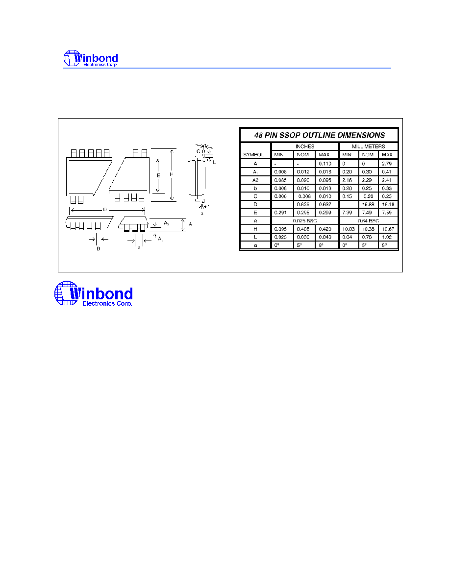
10.0 PACKAGE DRAWING AND DIMENSIONS
Headquarters
No. 4, Creation Rd. III
Science-Based Industrial Park
Hsinchu, Taiwan
TEL: 886-35-770066
FAX: 886-35-789467
www: http://www.winbond.com.tw/
Taipei Office
11F, No. 115, Sec. 3, Min-Sheng East Rd.
Taipei, Taiwan
TEL: 886-2-7190505
FAX: 886-2-7197502
TLX: 16485 WINTPE
Winbond Electronics (H.K.) Ltd.
Rm. 803, World Trade Square, Tower II
123 Hoi Bun Rd., Kwun Tong
Kowloon, Hong Kong
TEL: 852-27516023-7
FAX: 852-27552064
Winbond Electronics
(North America) Corp.
2730 Orchard Parkway
San Jose, CA 95134 U.S.A.
TEL: 1-408-9436666
FAX: 1-408-9436668
Please note that all data and specifications are subject to change without notice. All the
trade marks of products and companies mentioned in this data sheet belong to their
respective owners.
These products are not designed for use in life support appliances, devices, or systems
where malfunction of these products can reasonably be expected to result in personal
injury. Winbond customers using or selling these products for use in such applications
do so at their own risk and agree to fully indemnify Winbond for any damages resulting
from such improper use or sale.