
W83196R-718
W83196G-718
VIA BUFFER CHIP (4 X DDR or 2 X
DDR + 3 X SDRAM)
Date: Jan/23/2006 Revision: 2.2

W83196R-718/W83196G-718
Publication Release Date: January, 2006
- I - Revision 2.2
W83196R-718/W83196G-718 Data Sheet Revision History
PAGES
DATES
VERSION
WEB
VERSION
MAIN CONTENTS
1
n.a.
n.a.
All of the versions before 0.50 are for
internal use.
2
n.a
7/01/02
1.0
1.0
Change version and version on web site to
1.0
3
All
2/21/03
2.0
1.0
Update new form
4
4.6 12/18/03 2.1
1.0 Correction
IC
version, add register default
value and correction some description and
default value
5
01/23/06 2.2
2.2 Add
lead-free part number W83196G-718
6
7
8
9
10
Please note that all data and specifications are subject to change without notice. All
the trademarks of products and companies mentioned in this data sheet belong to
their respective owners.
LIFE SUPPORT APPLICATIONS
These products are not designed for use in life support appliances, devices, or
systems where malfunction of these products can reasonably be expected to result
in personal injury. Winbond customers using or selling these products for use in such
applications do so at their own risk and agree to fully indemnify Winbond for any
damages resulting from such improper use or sales.

W83196R-718/W83196G-718
-II-
Table of Content-
1.
GENERAL DESCRIPTION ......................................................................................................... 1
2.
PRODUCT FEATURES .............................................................................................................. 1
3.
PIN CONFIGURATION ............................................................................................................... 2
4.
BLOCK DIAGRAN....................................................................................................................... 3
5.
PIN DESCRIPTION..................................................................................................................... 4
5.1
Pin Description .........................................................................................................................4
5.2
Power Pins................................................................................................................................5
6.
I2C CONTROL AND STATUS REGISTERS .............................................................................. 6
6.1
Register 6: Output Control (1 = Enable, 0 = Disable) (Default = FFH)...................................6
6.2
Register 7: Output Control (1 = Enable, 0 = Disable) (Default = FFH)...................................6
7.
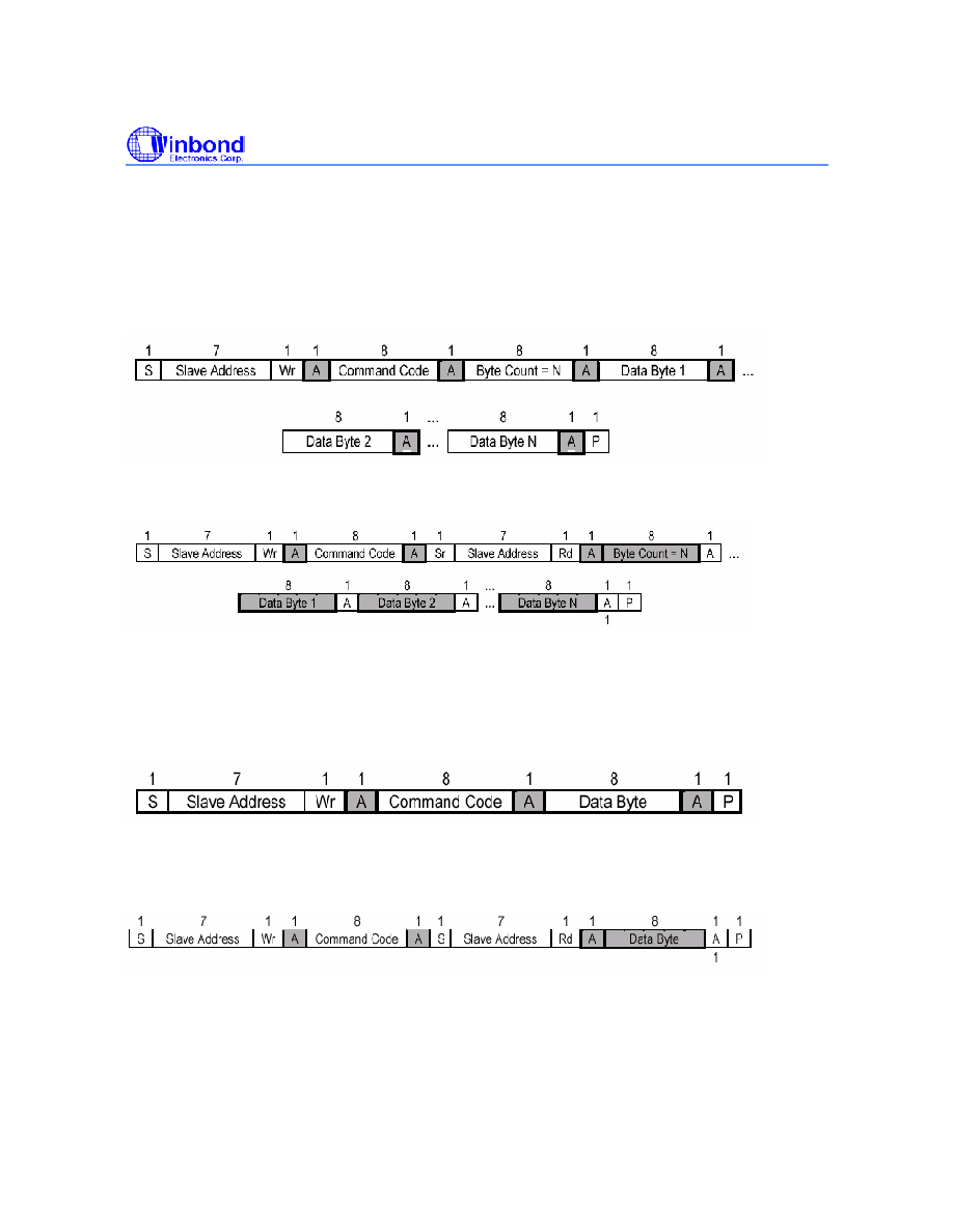
ACCESS INTERFACE ................................................................................................................ 7
7.1
Block Write protocol .................................................................................................................7
7.2
Block Read protocol .................................................................................................................7
7.3
Byte Write protocol ...................................................................................................................7
7.4
Byte Read protocol...................................................................................................................7
8.
SPECIFICATIONS ...................................................................................................................... 8
8.1
ABSOLUTE MAXIMUM RATINGS .........................................................................................8
9.
ORDERING INFORMATION....................................................................................................... 8
10.
HOW TO READ THE TOP MARKING........................................................................................ 9
11.
PACKAGE DRAWING AND DIMENSIONS.............................................................................. 10

W83196R-718/W83196G-718
Publication Release Date: January, 2006
- 1 - Revision 2.2
1. GENERAL
DESCRIPTION
The W83196R-718 is a 2.5V/3.3V Clock buffer. W83196R_718 can support 4 D.D.R. DRAM DIMMs or
3 standard SDRAM and 2 D.D.R. DRAM DIMMs.
W83196R-718 can be incorporated with W83194BR-P4X or W83194BR-325.
The W83196R_718 provides I
2
C serial bus interface to program the registers to enable or disable
each clock outputs. The W83196R_718 accepts a reference clock as its input and runs on a 3.3V or
2.5V supply.
2. PRODUCT
FEATURES
� One input to 24 outputs buffer
� Supports up to 4 D.D.R. DIMMs or 3 SDRAM DIMMs and 2 D.D.R. DIMMs
� One additional output for feedback
� Low Skew outputs (< 100ps)
� Supports up to 200MHz D.D.R. SDRAM
� I
2
C 2-Wire serial interface and supports Byte or Block Date RW
� Power management pin for power down control
� 48-pin SSOP package

W83196R-718/W83196G-718
-2-
3. PIN
CONFIGURATION
48
47
46
45
44
43
42
41
40
39
38
37
36
35
34
33
32
31
30
29
28
27
26
25
1
2
3
4
5
6
7
8
9
10
11
12
13
14
15
16
17
18
19
20
21
22
23
24
FB_output
Vss
DDR5T_SDRAM10
DDR0C_SDRAM1
PD#*
DDR7C
DDR6T
Vss
DDR11T
Vss
Vdd2.5
DDR9T
Vdd2.5
DDR9C
SEL_DDR*
Vss
DDR8C
Vss
DDR8T
DDR7T
SDATA*
Vdd3.3_2.5
DDR1T_SDRAM2
Buffer_IN
DDR5C_SDRAM11
SCLK*
DDR6C
Vdd2.5
Vss
Vdd2.5
DDR10C
DDR10T
DDR11C
Vdd3.3_2.5
DDR0T_SDRAM0
DDR1C_SDRAM3
Vdd3.3_2.5
Vss
DDR2T_SDRAM4
DDR2C_SDRAM5
Vdd3.3_2.5
Vss
DDR3T_SDRAM6
DDR3C_SDRAM7
Vdd3.3_2.5
Vss
DDR4T_SDRAM8
DDR4C_SDRAM9
*: Internal pull-up resistor 120K to Vdd3.3_2.5
#: Active low
W83196R-718/W83196G-718
Publication Release Date: January, 2006
- 3 - Revision 2.2
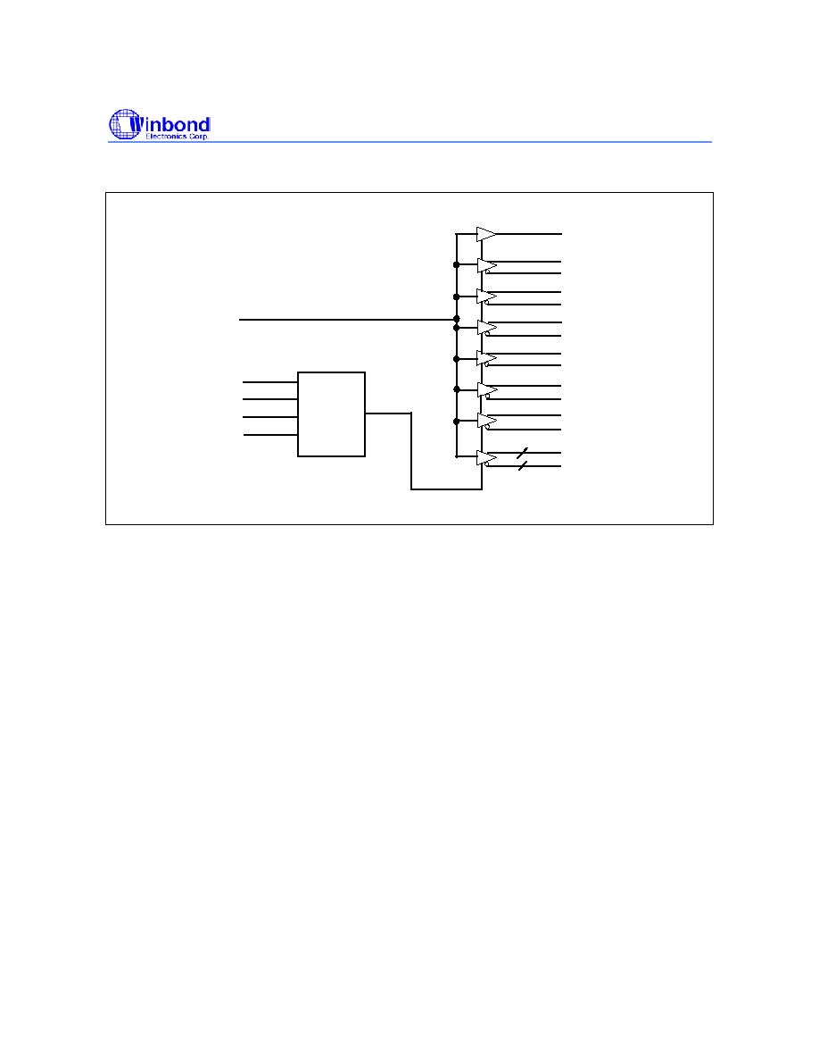
4. BLOCK
DIAGRAN
DDRT0_SDRAM0
FB_OUT
DDRC0_SDRAM1
DDRT1_SDRAM2
DDRC1_SDRAM3
DDRC2_SDRAM5
DDRT3_SDRAM6
DDRC3_SDRAM7
DDRT2_SDRAM4
DDRT4_SDRAM8
DDRC4_SDRAM9
DDRT5_SDRAM10
DDRC5_SDRAM11
DDRC(11:6)
DDRT(11:6)
Control
Logic
SCLK*
SDATA*
SEL_DDR*
PD#*
BUF_IN
6
6
W83196R-718/W83196G-718
-4-
5. PIN
DESCRIPTION
BUFFER TYPE SYMBOL
DESCRIPTION
IN Input
OUT Output
I/O Bi-directional
Pin
#
Active Low
*
Internal 120K
pull-up
5.1 Pin
Description
PIN
PIN NAME
TYPE
DESCRIPTION
48 SEL_DDR*
IN
1= DDR only mode
0=Standard SDRAM mode
When SEL_DDR is pulled high. Pin
4,5,6,7,10,11,15,16,19,20,21,
22,27,28,29,30,33,34,38,39,42,43,44 and 45 will be D.D.R.
outputs. Vdd3.3_2.5 should be connected to 2.5V for DDR
power supply.
When SEL_DDR is pulled low.
Pin 4,5,6,7,10,11,15,16,19, 20,21 and 22 will be standard
SDRAM outputs.
Pin 27,28,29,30,33,34,38,39,42,43,44 and 45 will be DDR
outputs,
Vdd3.3_2.5 should be connected to 3.3V for SDRAM.
24 SDATA* I/O
Serial data of I
2
C 2-wire control interface
Internal pull-up resistor 120K to Vdd3.3_2.5
25 SCLK* IN
Serial clock of I
2
C 2-wire control interface
Internal pull-up resistor 120K to Vdd3.3_2.5
13 Buffer_IN
IN
Reference input from chipset. 2.5V input for DDR only
mode. 3.3V for standard SDRAM mode.
1 FB_output
OUT
Feedback clock for chipset. Output voltage depends on
Vdd3.3_2.5
36 PD#*
IN
Active LOW input to enable Power Down mode and
All outputs will be Three-Stated
Internal pull-up resistor 120K to Vdd3.3_2.5
28,30,34,39,43,45 DDR [6:11] T OUT Clock outputs. Copies of Buffer_IN.
27,29,33,38,42,44 DDR [6:11] C OUT Complementary copies of Buffer_IN
4,6,10,15,19,
21
DDR [0:5]
T_SDRAM
[0,2,4,6,8,10]
OUT
Clock outputs.
SEL_DDR=1, these pins are copies of Buffer_IN.
SEL_DDR=0, these pins are copies of Buffer_IN.
Voltage depends on the Vdd3.3_2.5
5,7,11,16,20
22
DDR [0:5]
C_SDRAM
[1,3,5,7,9,11]
OUT
Clock outputs.
SEL_DDR=1, these pins are complementary copies of
Buffer_IN.
SEL_DDR=0, these pins are copies of Buffer_IN.
Voltage depends on the Vdd3.3_2.5
W83196R-718/W83196G-718
Publication Release Date: January, 2006
- 5 - Revision 2.2
5.2 Power
Pins
PIN
PIN NAME
DESCRIPTION
2,8,12,17,23 Vdd3.3_2.5
Connected to 2.5V when SEL_DDR=1 and 3.3V when
SEL_DDR=0
32,37,41,47
Vdd2.5
Power supply 2.5V.
3,9,14,18,26,31,35,
40,46
Vss Ground
W83196R-718/W83196G-718
-6-
6. I2C CONTROL AND STATUS REGISTERS
Note: The Register 1~5 is reserved for main clock
6.1 Register 6: Output Control (1 = Enable, 0 = Disable) (Default = FFH)
BIT
@POWERUP
PIN
DESCRIPTION
7
1 48
SEL_DDR (Read back only)
6:5
11
-
Reserved for Winbond internal use, do not change them
4 1 -
When the pin is low �level, Pin
27,28,29,30,32,33,34,,38,39,42,43
, 44,45 will be Three-Stated in the SDRAM Mode.
3 1
45,44
DDR11T,
DDR11C
output control
2 1
43,42
DDR10T,
DDR10C
output control
1 1
39,38
DDR9T,
DDR9C
output control
0 1
34,33
DDR8T,
DDR8C
output control
6.2 Register 7: Output Control (1 = Enable, 0 = Disable)
(Default = FFH)
BIT
@POWERUP
PIN
DESCRIPTION
7 1
30,39
DDR7T,
DDR7C
output control
6 1
28,27
DDR6T,
DDR6C
output control
5 1
21,22
DDR5T_SDRAM10,
DDR5C_SDRAM11
output control
4 1
19,20
DDR4T_SDRAM8,
DDR4C_SDRAM9
output control
3 1
15,16
DDR3T_SDRAM6,
DDR3C_SDRAM7
output control
2 1
10,11
DDR2T_SDRAM4,
DDR2C_SDRAM5
output control
1 1 6,7
DDR1T_SDRAM2,
DDR1C_SDRAM3
output control
0 1 4,5
DDR0T_SDRAM0,
DDR0C_SDRAM1
output control
W83196R-718/W83196G-718
Publication Release Date: January, 2006
- 7 - Revision 2.2
7. ACCESS
INTERFACE
The W83196R-718 provides I
2
C Serial Bus for microprocessor to read/write internal registers. In the
W83196R-718 is provided Block Read/Block Write and Byte-Data Read/Write protocol. The I
2
C
address is defined at 0xD2.
7.1 Block Write protocol
7.2 Block Read protocol
## In block mode, the command code must filled 8'h00
7.3 Byte Write protocol
7.4 Byte
Read
protocol

W83196R-718/W83196G-718
-8-
8. SPECIFICATIONS
8.1 ABSOLUTE MAXIMUM RATINGS
Stresses greater than those listed in this table may cause permanent damage to the device.
Precautions should be taken to avoid application of any voltage higher than the maximum rated
voltages to this circuit. Subjection to maximum conditions for extended periods may affect reliability.
Unused inputs must always be tied to an appropriate logic voltage level (Ground or Vdd).
PARAMETER RATING
Supply Voltage (Vdd=3.3V)
3.0V ~ 3.6V
Supply Voltage (Vdd=2.5V)
2.3V ~2.7V
Storage Temperature
- 65
�C to + 150�C
Ambient Temperature
- 55
�C to + 125�C
Operating Temperature
0
�C to + 70�C
Input ESD protection (Human body model)
2000V
9. ORDERING
INFORMATION
PART NUMBER
PACKAGE TYPE
PRODUCTION FLOW
W83196R-718
48 PIN SSOP
Commercial, 0
�C to +70�C
W83196G-718
48 PIN SSOP (Pb-free package)
Commercial, 0
�C to +70�C
W83196R-718/W83196G-718
Publication Release Date: January, 2006
- 9 - Revision 2.2
10. HOW TO READ THE TOP MARKING
1st line: Winbond logo and the type number: W83196R-718/W83196G-718
2nd line: Tracking code 2 8051234
2: wafers manufactured in Winbond FAB 2
8051234: wafer production series lot number
3rd line: Tracking code 342 G AA
342: packages made in '2003, week 42
G: assembly house ID; O means OSE, G means GR
A: Internal use code
A
: IC revision
All the trade marks of products and companies mentioned in this data sheet belong to their
respective owners.
W83196R-718
28051234
342GA
A
W83196G-718
28051234
342GA
A
W83196R-718/W83196G-718
-10-
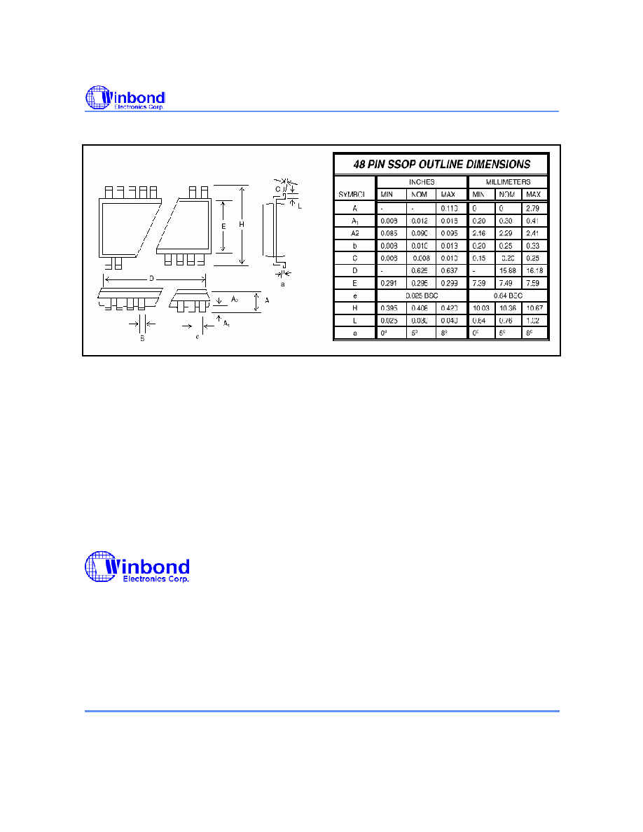
11. PACKAGE DRAWING AND DIMENSIONS
Important Notice
Winbond products are not designed, intended, authorized or warranted for use as components
in systems or equipment intended for surgical implantation, atomic energy control
instruments, airplane or spaceship instruments, transportation instruments, traffic signal
instruments, combustion control instruments, or for other applications intended to support or
sustain life. Further more, Winbond products are not intended for applications wherein failure
of Winbond products could result or lead to a situation wherein personal injury, death or
severe property or environmental damage could occur.
Winbond customers using or selling these products for use in such applications do so at their
own risk and agree to fully indemnify Winbond for any damages resulting from such improper
use or sales.
Headquarters
No. 4, Creation Rd. III,
Science-Based Industrial Park,
Hsinchu, Taiwan
TEL: 886-3-5770066
FAX: 886-3-5665577
http://www.winbond.com.tw/
Taipei Office
TEL: 886-2-8177-7168
FAX: 886-2-8751-3579
Winbond Electronics Corporation America
2727 North First Street, San Jose,
CA 95134, U.S.A.
TEL: 1-408-9436666
FAX: 1-408-5441798
Winbond Electronics (H.K.) Ltd.
No. 378 Kwun Tong Rd.,
Kowloon, Hong Kong
FAX: 852-27552064
Unit 9-15, 22F, Millennium City,
TEL: 852-27513100
Please note that all data and specifications are subject to change without notice.
All the trade marks of products and companies mentioned in this data sheet belong to their respective owners.
Winbond Electronics (Shanghai) Ltd.
200336 China
FAX: 86-21-62365998
27F, 2299 Yan An W. Rd. Shanghai,
TEL: 86-21-62365999
Winbond Electronics Corporation Japan
Shinyokohama Kohoku-ku,
Yokohama, 222-0033
FAX: 81-45-4781800
7F Daini-ueno BLDG, 3-7-18
TEL: 81-45-4781881
9F, No.480, Rueiguang Rd.,
Neihu District, Taipei, 114,
Taiwan, R.O.C.