
Winbond
Integrated Media Reader
W83L519D

W83L519D
The trademarks and intellectual property rights of Memory Stick belong to SONY Corporation
Publication Release Date: Jul. 2002
The trademarks and intellectual property rights of SD belong to SD GROUP
Revision 1.0
All trademarks and brand names belong to their respective owners
1
W83L519D
Datasheet Revision History
Pages Dates Version Version
on Web
Main Contents
1 02/Jul. 1.0 1.0 1
st
Release
2
02/Sep.
1.01 1.01
Remove GPIO function and modify recommend
circuit.
3
4
5
6
7
8
Please note that all data and specifications are subject to change without notice. All the
trademarks of products and companies mentioned in this data sheet belong to their
respective owners.
LIFE SUPPORT APPLICATIONS
These products are not designed for use in life support appliances, devices, or systems
where malfunction of these products can reasonably be expected to result in personal
injury. Winbond customers using or selling these products for use in such applications
do so at their own risk and agree to fully indemnify Winbond for any damages resulting
from such improper use or sales.

W83L519D
The trademarks and intellectual property rights of Memory Stick belong to SONY Corporation
Publication Release Date: Jul. 2002
The trademarks and intellectual property rights of SD belong to SD GROUP
Revision 1.0
All trademarks and brand names belong to their respective owners
2
CONTENT
1
GENERAL DESCRIPTION...............................................................................................................3
2
FUNCTIONS .....................................................................................................................................4
2.1
G
ENERAL
........................................................................................................................................4
2.2
S
MART
C
ARD
I
NTERFACE
.................................................................................................................4
2.3
M
EMORY
S
TICK
I
NTERFACE
..............................................................................................................4
2.4
SD M
EMORY
C
ARD
I
NTERFACE
........................................................................................................4
2.5
P
ACKAGE
........................................................................................................................................4
3
PIN CONFIGURATION ....................................................................................................................5
4
PIN DESCRIPTION ..........................................................................................................................6
4.1
B
US
I
NTERFACE
...............................................................................................................................6
4.2
S
MART
C
ARD
I
NTERFACE
P
INS
.........................................................................................................7
4.3
M
EMORY
S
TICK
I
NTERFACE
/SD M
EMORY
I
NTERFACE
P
INS
................................................................8
4.4
C
RYSTAL AND
P
OWER
P
INS
..............................................................................................................9
5
CONFIGURATION REGISTER ......................................................................................................10
5.1
P
LUG AND
P
LAY
C
ONFIGURATION
...................................................................................................10
5.2
C
OMPATIBLE
P
N
P..........................................................................................................................10
5.2.1
Extended Function Register ................................................................................................10
5.2.2
Extended Functions Enable Register (EFER) .....................................................................11
5.2.3
Extended Function Index Register (EFIR), Extended Function Data Register (EFDR) ......11
5.3
C
ONFIGURATION
S
EQUENCE
..........................................................................................................11
5.3.1
Software programming example..........................................................................................12
5.4
G
LOBAL
R
EGISTERS
......................................................................................................................12
5.5
L
OGICAL
D
EVICE
0 (S
MART
C
ARD
I
NTERFACE
)................................................................................14
5.6
L
OGICAL
D
EVICE
1 (M
EMORY
S
TICK
I
NTERFACE
) ............................................................................15
5.7
L
OGICAL
D
EVICE
3 (SD M
EMORY
I
NTERFACE
) ..............................................................................15
5
6
ORDERING INSTRUCTION.........................................................................................................17
6
7
HOW TO READ THE TOP MARKING.........................................................................................17
6
8
PACKAGE DRAWING AND DIMENSIONS ..................................................................................
17
9
THE W83L519D SCHEMATIC .......................................................................................................
18

W83L519D
The trademarks and intellectual property rights of Memory Stick belong to SONY Corporation
Publication Release Date: Jul. 2002
The trademarks and intellectual property rights of SD belong to SD GROUP
Revision 1.0
All trademarks and brand names belong to their respective owners
3
1 GENERAL
DESCRIPTION
W83L519D is Winbond's innovative solution to a new class of storage devices for IA Noetebook, Desktop
PC and PC system-related products. It incorporates a security Application: Smart Card Interface and two
most promising compact storage interfaces: Memory Stick interface, and Secure Digital Memory Card
interface in IT era.
To cater boundless IT implementation possibilities, W83L519D can be configured to interface with host
through ISA bus. Base on the ISA interface, one Smart Card Interface port and an optional Memory
Stick/SD memory Interface ports are provided. The kind of versatility allows user to design very cost-
effective products in a very flexible way.
The whole chip of W83L519D operates at voltage level of 3.3 V except Smart Card Interface port's I/O
pins and ISA bus interface that are at 5 V to be compatible with mainstream Smart Card implementations.
Advanced power management feature further optimizes power consumption whether in operation or in
power down mode.
W83L519D comes as a 48-pin LQFP streamline package. Combining with powerful functions, effective
power management, and versatile configurability, this integrated media reader offers a perfect approach
for design of storage device of IT products.
The trademarks and intellectual property rights of Memory Stick belong to SONY Corporation. Information
check: http://www.memorystick.org/
The trademarks and intellectual property rights of Secure Digital belong to SD Group. Information check:
http://www.sdcard.org/

W83L519D
The trademarks and intellectual property rights of Memory Stick belong to SONY Corporation
Publication Release Date: Jul. 2002
The trademarks and intellectual property rights of SD belong to SD GROUP
Revision 1.0
All trademarks and brand names belong to their respective owners
4
2 FUNCTIONS
2.1 General
Support ISA bus
Programmable configuration settings
48 MHz crystal inputs
2.2 Smart Card Interface
ISO-7816 compliant
PC/SC T=0, T=1 compliant
16-byte transmitter FIFO and 16-byte receiver FIFO
FIFO threshold interrupt to optimize system performance
Programmable transmission clock frequency
Versatile baud rate configuration
UART-like register file structure
2.3 Memory
Stick
Interface
Memory Stick Standard Format Specifications ver. 1.3 compliant
Support interrupt polling transmission
Support FIFO threshold interrupt to optimize system performance
Automatic clock halt to prevent underrun/overrun
16 MHz interface clock
2.4 SD Memory Card Interface
SD Memory Card Specifications: Part 1 PHYSICAL LAYER SPECIFICATION Version 1.0
Compliant
Support interrupt polling transmission
Support FIFO threshold interrupt to leverage system performance
24 MHz interface clock
2.5 Package
48-pin LQFP
W83L519D
The trademarks and intellectual property rights of Memory Stick belong to SONY Corporation
Publication Release Date: Jul. 2002
The trademarks and intellectual property rights of SD belong to SD GROUP
Revision 1.0
All trademarks and brand names belong to their respective owners
5
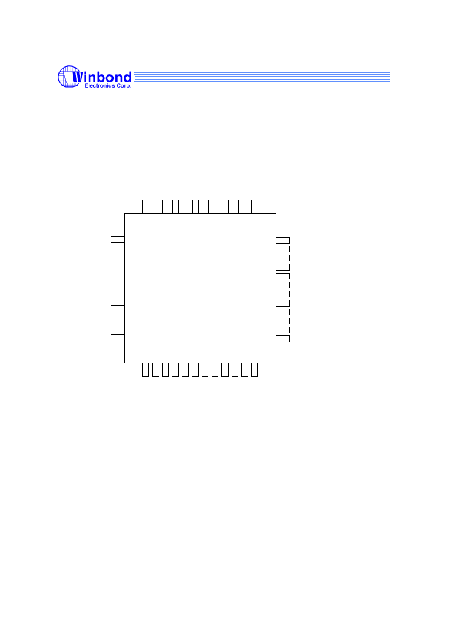
3 PIN CONFIGURATION
W83L519D
IRQ
A
IOR
#
IOW
#
RE
SE
T
#
PM
E
#
VS
S
D7
D6
D5
D4
D3
D2
1
2
3
4
5
6
7
8
9
10
11
12
36
35
34
33
32
31
30
29
28
27
26
25
A
EN
TC
DACK
#
DRQ
MS
LED/S
D
LE
D/SD_W
P
MS
PW
R#/SDP
W
R
#
VS
S
M
S
C
L
K
/
SD
C
L
K
MS
1/SD1
MS
2/SD2
MS
3/SD3
MS
4/SD4
A9
A8
A7
VDD3V
A6
A5
A4
A3
A2
A1
A0
IRQB
MS5/SD5
XIN
XOUT
SCRST#
SCIO
SCCLK
SCPSNT
SCPWR#
SCLED
VDD
D0
D1
24
23
22
21
20
19
18
17
16
15
14
13
37
38
39
40
41
42
43
44
45
46
47
48

W83L519D
The trademarks and intellectual property rights of Memory Stick belong to SONY Corporation
Publication Release Date: Jul. 2002
The trademarks and intellectual property rights of SD belong to SD GROUP
Revision 1.0
All trademarks and brand names belong to their respective owners
6
4 PIN DESCRIPTION
Note:
INtp3
- 3.3V TTL level input pin
INts
- 5V TTL level Schmitt-trigger input pin
INtsp3
- 3.3V TTL level Schmitt-trigger input pin
I/O12t
- 5V TTL level bi-directional pin with 12 mA drive-sink capability
I/O24t
- 5V TTL level bi-directional pin with 24 mA drive-sink capability
I/O24tp3
- 3.3V TTL level bi-directional pin with 24 mA drive-sink capability
O2
- 5V output pin with 2 mA drive-sink capability
O12
- 5V output pin with 12 mA drive-sink capability
O24p3
- 3.3V output pin with 24 mA drive-sink capability
OD12
- Open-drain output pin with 12 mA sink capability
4.1 Bus
Interface
SYMBOL PIN I/O
FUNCTION
RESET#
4 IN
tsp3
Active-low system reset signal.
IOW#
3 IN
tsp3
ISA configuration: Active-low signal to enable ISA I/O write
accesses.
IOR# 2
IN
tsp3
ISA configuration: Active-low signal to enable ISA I/O read
accesses.
IRQA 1
O
24p3
ISA configuration: Interrupt output of Smart Card interface port.
IRQB 48
O
24p3
ISA configuration: Interrupt output of Memory Stick/SD Memory
Card interface port.
A0 47
IN
tp3
ISA configuration: Address bit 0.
A1 46
IN
tp3
ISA configuration: Address bit 1.
A2 45
IN
tp3
ISA configuration: Address bit 2.
A3 44
IN
tp3
ISA configuration: Address bit 3.
A4 43
IN
tp3
ISA configuration: Address bit 4.
A5 42
IN
tp3
ISA configuration: Address bit 5.
A6 41
IN
tp3
ISA configuration: Address bit 6.
A7 39
IN
tp3
ISA configuration: Address bit 7.
A8 38
IN
tp3
ISA configuration: Address bit 8.
A9 37
IN
tp3
ISA configuration: Address bit 9.

W83L519D
The trademarks and intellectual property rights of Memory Stick belong to SONY Corporation
Publication Release Date: Jul. 2002
The trademarks and intellectual property rights of SD belong to SD GROUP
Revision 1.0
All trademarks and brand names belong to their respective owners
7
4.1 Bus Interface (continued.)
SYMBOL PIN I/O
FUNCTION
AEN
36 IN
tp3
ISA configuration: Active-low I/O address enable signal. It is
pulled high in DMA accesses.
TC 35
IN
tp3
ISA configuration: This pin signals termination of DMA accesses.
DACK#
34 IN
tp3
ISA configuration: DMA acknowledge. This active-low signal
validates DMA accesses.
DRQ 33
O
24p3
ISA configuration: DMA request signal.
D7 7
I/O
12t
ISA configuration: System data bit 7.
D6 8
I/O
12t
ISA configuration: System data bit 6.
D5 9
I/O
12t
ISA configuration: System data bit 5.
D4 10
I/O
12t
ISA configuration: System data bit 4.
D3 11
I/O
12t
ISA configuration: System data bit 3.
D2 12
I/O
12t
ISA configuration: System data bit 2.
D1 13
I/O
24t
ISA configuration: System data bit 1.
D0 14
I/O
24t
ISA configuration: System data bit 0.
PME#
5 OD
12
Active-low
PME
event.
4.2 Smart Card Interface Pins
SYMBOL PIN I/O
FUNCTION
SCLED 16
O
24
This pin outputs an oscillating clock signal of various frequencies
depending on traffic of primary Smart Card interface.
SCPWR# 17 O
24
Primary Smart Card interface power control signal.
SCPSNT 18
IN
ts
Primary Smart Card interface card present detection Schmitt-
trigger input.
SCCLK 19
O
2
Primary Smart Card interface clock output.
SCIO 20
I/O
12t
Primary Smart Card interface data I/O channel.
SCRST# 21
O
12
Primary Smart Card interface reset output.

W83L519D
The trademarks and intellectual property rights of Memory Stick belong to SONY Corporation
Publication Release Date: Jul. 2002
The trademarks and intellectual property rights of SD belong to SD GROUP
Revision 1.0
All trademarks and brand names belong to their respective owners
8
4.3 Memory Stick Interface/SD Memory Interface Pins
SYMBOL PIN I/O
FUNCTION
MSLED
SDLED
SD_WP
32 O
24p3
O
24p3
IN
ts
MS/SD select = 0, MS function - This pin outputs an oscillating
clock signal of various frequencies depending on traffic of
primary Memory Stick interface;
MS/SD select = 1, SD function - This pin outputs an oscillating
clock signal of various frequencies depending on traffic of
primary SD memory card interface.
MS/SD select = 1, SD function � Write protect input signal.
MSPWR#
SDPWR#
31 O
24p3
O
24p3
MS/SD select = 0, MS function - This pin is power control signal
for primary Memory Stick interface;
MS/SD select = 1, SD function - This pin is power control signal
for primary SD memory card interface.
MSCLK
SDCLK
29 O
24p3
O
24p3
MS/SD select = 0, MS function - This pin is SCLK for primary
Memory Stick interface;
MS/SD select = 1, SD function - This pin is CLK for primary SD
memory card interface.
MS1
SD1
28 O
24p3
I/O
24tp3
MS/SD select = 0, MS function - This pin is MS1 for primary
Memory Stick interface;
MS/SD select = 1, SD function - This pin is SD1 for primary SD
memory card interface.
MS2
SD2
27 I/O
24tp3
I/O
24tp3
MS/SD select = 0, MS function - This pin is MS2 for primary
Memory Stick interface;
MS/SD select = 1, SD function - This pin is SD2 for primary SD
memory card interface.
MS3
SD3
26 ---
I/O
24tp3
MS/SD select = 0, MS function - This pin is MS3 for primary
Memory Stick interface;
MS/SD select = 1, SD function - This pin is SD3 for primary SD
memory card interface.
MS4
SD4
25 IN
tsp3
I/O
24tp3
MS/SD select = 0, MS function - This pin is MS4 for primary
Memory Stick interface;
MS/SD select = 1, SD function - This pin is SD4 for primary SD
memory card interface.
W83L519D
The trademarks and intellectual property rights of Memory Stick belong to SONY Corporation
Publication Release Date: Jul. 2002
The trademarks and intellectual property rights of SD belong to SD GROUP
Revision 1.0
All trademarks and brand names belong to their respective owners
9
4.3 Memory Stick Interface/SD Memory Interface Pins (Continued.)
SYMBOL PIN I/O
FUNCTION
MS5
SD5
24 ---
I/O
24tp3
MS/SD select = 0, MS function - This pin is MS5 for primary
Memory Stick interface;
MS/SD select = 1, SD function - This pin is SD5 for primary SD
memory card interface.
4.4 Crystal and Power Pins
SYMBOL PIN
FUNCTION
XOUT, XIN
22, 23
Connected to a 48 MHz crystal and function as the working
clock for all the media reader interfaces.
VDD3V
40
+3.3V power supply for host interface, MSI/SDI interfaces, and
internal core.
VDD
15
+5V power supply for Smart Card interface I/O pins.
VSS
6, 30
Ground.

W83L519D
The trademarks and intellectual property rights of Memory Stick belong to SONY Corporation
Publication Release Date: Jul. 2002
The trademarks and intellectual property rights of SD belong to SD GROUP
Revision 1.0
All trademarks and brand names belong to their respective owners
10
5 CONFIGURATION
REGISTER
5.1 Plug and Play Configuration
W83L519D implement compatible PNP protocol to access configuration registers for setting up
different types of configurations. There are three Logical Devices (Logical Device 0 to Logical Device
2) in W83L518D/W83L519D which correspond to three major functions: Smart Card Interface (logical
device 0), Memory Stick Interface/SD memory Interface (logical device 1), GPIO (logical device 2).
Each Logical Device has its own configuration registers (CR30 and above). Host can access those
registers by writing an appropriate logical device number into logical device select register at CR7 first.
One set per
logical device
logical device select
07h
30h
40h
FEh
3Fh
logical device control
global registers
logical device
configuration
5.2 Compatible
PnP
5.2.1 Extended
Function
Register
W83L518D/W83L519D provide two methods to enter Extended Function mode (compatible PnP)
and access configuration registers dependent on value of HEFRAS (bit 6 of CR26) as follows:
HEFRAS
address and value
0
write 83h to I/O address 2Eh twice
1
write 83h to I/O address 4Eh twice
In Compatible PnP, a specific value (83h) must be written twice to the Extended Function Enable
Register (EFER at I/O address 2Eh or 4Eh). Secondly, an index value (02h, 07h-FFh) must be
written to the Extended Function Index Register (EFIR, I/O address at 2Eh or 4Eh which is the same
as EFER) to identify which configuration register is to be accessed. User can then access the
addressed configuration register through the Extended Function Data Register (EFDR, I/O address
at 2Fh or 4Fh).

W83L519D
The trademarks and intellectual property rights of Memory Stick belong to SONY Corporation
Publication Release Date: Jul. 2002
The trademarks and intellectual property rights of SD belong to SD GROUP
Revision 1.0
All trademarks and brand names belong to their respective owners
11
After programming of the configuration register is completed, another specific value (AAh) should be
written to EFER to leave Extended Function mode to prevent inadvertent accesses to those
configuration registers. User may write a "1" to bit 5 of CR26 (LOCKREG) to prevent configuration
registers from accidental accesses.
5.2.2 Extended Functions Enable Register (EFER)
After a power-on reset, W83L518D/W83L519D enters the default operation mode. A specific value
must be programmed into the Extended Function Enable Register (EFER) so that configuration
registers can be accessed. On a PC/AT system, its I/O address is 2Eh or 4Eh (as described in
previous section).
5.2.3 Extended Function Index Register (EFIR), Extended Function Data Register (EFDR)
After entering Extended Function mode, Extended Function Index Register (EFIR) must be written
with an index value (02h, 07h-FEh) to specify which configuration register is to be accessed through
Extended Function Data Register (EFDR). EFIR is a write-only register at I/O address 2Eh or 4Eh
(as described in section 6.2.1) on a PC/AT system and EFDR is a read/write register at I/O address
2Fh or 4Fh.
5.3 Configuration
Sequence
To program configuration registers, specific configuration sequence must be followed:
(1) Write 83h to EFER twice to enter Extended Function mode.
(2) Select logical device select register by writing 07h to EFIR.
(3) Select logical device by writing a value to EFDR.
(4) Select control/configuration register by writing its index to EFIR.
(5) Access selected control/configuration register through EFDR.
(6) Repeat step 4 ~ 5 as needed.
(7) Leave Extended Function mode by writing AAh to EFER.
Step 2 and step 3 are not necessary for accessing global register (index 00h to 2Fh).

W83L519D
The trademarks and intellectual property rights of Memory Stick belong to SONY Corporation
Publication Release Date: Jul. 2002
The trademarks and intellectual property rights of SD belong to SD GROUP
Revision 1.0
All trademarks and brand names belong to their respective owners
12
5.3.1 Software
programming
example
The following example is written in Intel 8086 assembly language. EFER and EFIR are assumed to
be at 2Eh, and EFDR is at 2Fh. Use 4Eh/4Fh instead of 2Eh/2Fh if HEFRAS (bit 6 of CR26) is set.
;-----------------------------------------------------------------------------------
; Enter Extended Function mode, interruptible double-write |
;-----------------------------------------------------------------------------------
MOV DX,
2Eh
MOV AL,
83h
OUT DX,
AL
OUT DX,
AL
;-----------------------------------------------------------------------------
; Configure logical device 1, configuration register CRF0 |
;-----------------------------------------------------------------------------
MOV DX,
2Eh
MOV AL,
07h
OUT
DX, AL
; point to Logical Device Number Reg.
MOV DX,
2Fh
MOV AL,
01h
OUT
DX, AL
; select logical device 1
;
MOV DX, 2Eh
MOV AL,
F0H
OUT
DX, AL
; select CRF0
MOV DX,
2Fh
MOV AL,
3Ch
OUT
DX, AL
; update CRF0 with value 3CH
;------------------------------------------
; Exit extended function mode |
;------------------------------------------
MOV DX,
2Eh
MOV AL,
AAh
OUT DX,
AL
5.4 Global Registers
CR02 (Default 00h, write only)
Bit [7:1]: Reserved.
Bit 0: SWRST
= 0
Normal operation.
= 1
Software reset.
CR07 (Default 00h)
Bit [7:0]: Logical Device Number.
CR20 (read only)
Bit [7:0]: Device ID number (higher byte).
=
71h

W83L519D
The trademarks and intellectual property rights of Memory Stick belong to SONY Corporation
Publication Release Date: Jul. 2002
The trademarks and intellectual property rights of SD belong to SD GROUP
Revision 1.0
All trademarks and brand names belong to their respective owners
13
CR21 (read only)
Bit [7:0]: Device ID number (lower byte)
=
2Xh
CR22 (Default 80h)
Bit 7: SCPWD
=
0
Power down Smart Card interface.
=
1
No Power down.
Bit 6: MSPWD
=
0
Power down Memory Stick interface.
=
1
No Power down.
Bit 5: SDPWD
=
0
Power down SD memory card interface.
=
1
No Power down.
Bit [4:0]: Reserved.
CR23 (Default 00h)
Bit 7: PME_EN. Power management event enable bit.
=
0
PME_L function is disabled.
=
1
Enable to issue a low pulse on PME_L when a power management event occurs.
Bit 6: MSPME_EN. Memory Stick interface power management event enable bit.
=
0
Memory Stick interface power management event is disabled.
=
1
Enable Memory Stick interface power management event to issue a low pulse on
PME_L when PME_EN is also enabled.
Bit 5: SDPME_EN. SD memory card interface power management event enable bit.
=
0
SD memory card interface power management event is disabled.
=
1
Enable SD memory card interface power management event to issue a low pulse on
PME_L when PME_EN is also enabled.
Bit 4: SCPME_EN. Smart Card interface power management event enable bit.
=
0
Smart Card interface power management event is disabled.
=
1
Enable Smart Card interface power management event to issue a low pulse on
PME_L when PME_EN is also enabled.
Bit [3:0]: Reserved.
CR24 (Default 00h)
Bit 7: Reserved.
Bit 6: MSPME_STS. Memory Stick interface power management event status bit.

W83L519D
The trademarks and intellectual property rights of Memory Stick belong to SONY Corporation
Publication Release Date: Jul. 2002
The trademarks and intellectual property rights of SD belong to SD GROUP
Revision 1.0
All trademarks and brand names belong to their respective owners
14
=
0
No Memory Stick interface power management event occurs.
=
1
Memory Stick interface power management event occurs.
Bit 5: SDPME_STS. SD memory card interface power management event status bit.
=
0
No SD memory card interface power management event occurs.
=
1
SD memory card interface power management event occurs.
Bit 4: SCPME_STS. Smart Card interface power management event status bit.
=
0
No Smart Card interface power management event occurs.
=
1
No Smart Card interface power management event occurs.
Bit [3:0]: Reserved.
CR26 (Default 00h)
Bit 7: Reserved
Bit 6: HEFRAS, Extended Function Register Address Select.
= 0
Extended Function Registers are at 2Eh/2Fh.
= 1
Extended Function Registers are at 4Eh/4Fh.
Bit 5: LOCKREG
= 0
Enable accesses of Configuration Registers.
= 1
Disable accesses of Configuration Registers.
Bit [4:0]: Reserved
5.5 Logical Device 0 (Smart Card Interface)
CR30 (Default 0x00)
Bit
[7:1]:
Reserved.
Bit 0: Logical device active bit.
= 0
Logical device is inactive.
= 1
Activates the logical device.
CR60, CR61 (Default 0x00, 0x00)
These two registers select Smart Card base address [0x100:0xFFF] on 8-byte boundary.
CR70 (Default 0x00)
Bit [7:4]: Reserved.
Bit [3:0]: These bits select IRQ resource for Smart Card interface.
CRF0 (Default 0x00)
Bit [7:1]: Reserved.
Bit 0: SCPSNT_POL (Smart Card PreSeNT POLarity). SCPSNT polarity bit.
=
0
SCPSNT is active high.
= 1
SCPSNT is active low.

W83L519D
The trademarks and intellectual property rights of Memory Stick belong to SONY Corporation
Publication Release Date: Jul. 2002
The trademarks and intellectual property rights of SD belong to SD GROUP
Revision 1.0
All trademarks and brand names belong to their respective owners
15
5.6 Logical Device 1 (Memory Stick Interface)
CR30 (Default 0x00)
Bit [7:1]: Reserved.
Bit 0: Logical device active bit.
= 0: Logical device is inactive.
= 1: Activates the logical device.
CR60, CR61 (Default 0x00, 0x00)
These two registers select MSI base address [0x100:0xFFF] on 8-byte boundary.
CR70 (Default 0x00)
Bit [7:4]: Reserved.
Bit [3:0]: These bits select IRQ resource for MSI.
CR74 (Default 0x04)
Bit [7:4]: Reserved.
Bit [3:0]: These bits select DRQ resource for MSI.
5.7 Logical Device 3 (SD Memory Interface)
CR30 (Default 0x00)
Bit [7:1]: Reserved.
Bit 0: Logical device active bit.
= 0
Logical device is inactive.
= 1
Activates the logical device.
CR60, CR61 (Default 0x00, 0x00)
These two registers select SD Card interface base address [0x100:0xFFF] on 8-byte boundary.
CR70 (Default 0x00)
Bit
[7:4]:
Reserved.
Bit [3:0]: These bits select IRQ resource for SD interface.
CR74 (Default 0x00)
Bit
[7:4]:
Reserved.
Bit [3:0]: These bits select DRQ resource for SD interface.

W83L519D
The trademarks and intellectual property rights of Memory Stick belong to SONY Corporation
Publication Release Date: Jul. 2002
The trademarks and intellectual property rights of SD belong to SD GROUP
Revision 1.0
All trademarks and brand names belong to their respective owners
16

W83L519D
The trademarks and intellectual property rights of Memory Stick belong to SONY Corporation
Publication Release Date: Jul. 2002
The trademarks and intellectual property rights of SD belong to SD GROUP
Revision 1.0
All trademarks and brand names belong to their respective owners
17
6 ORDERING
INSTRUCTION
PART NO.
PACKAGE
REMARKS
W83L519D
48-pin LQFP
7 HOW TO READ THE TOP MARKING
1st line: Winbond logo and the SMART@IO Trademark
2nd line: The chip part number.
3rd line: Tracking code 114 G BSB
114: packages made in '01, week 14
G: assembly house ID; O means OSE, G means GR, ...
BSB: IC revision
S
MART@
IO
W83L519D
114GBSB

W83L519D
The trademarks and intellectual property rights of Memory Stick belong to SONY Corporation
Publication Release Date: Jul. 2002
The trademarks and intellectual property rights of SD belong to SD GROUP
Revision 1.0
All trademarks and brand names belong to their respective owners
18
8 PACKAGE DRAWING AND DIMENSIONS
Package- 48-pin LQFP
1
12
48
H
H
Controlling dimension : Millimeters
0.10
0
7
0
0.004
1.00
0.75
0.60
0.45
0.039
0.030
0.024
0.018
9.10
9.00
8.90
0.358
0.354
0.350
0.50
0.20
0.25
1.45
1.40
0.10
0.15
1.35
0.008
0.010
0.057
0.055
0.026
7.10
7.00
6.90
0.280
0.276
0.272
0.004
0.006
0.053
Symbol
Min Nom Max
Max
Nom
Min
Dimension in inch
Dimension in mm
A
b
c
D
e
H
D
H
E
L
Y
0
A
A
L
1
1
2
E
0.008
0.006
0.15
0.20
7
0.020
0.35
0.65
0.10
0.05
0.002 0.004
0.006
0.15
9.10
9.00
8.90
0.358
0.354
0.350
7.10
7.00
6.90
0.280
0.276
0.272
0.014
37
36
25
24
13

W83L519D
The trademarks and intellectual property rights of Memory Stick belong to SONY Corporation
Publication Release Date: Jul. 2002
The trademarks and intellectual property rights of SD belong to SD GROUP
Revision 1.0
All trademarks and brand names belong to their respective owners
19
9 THE W83L519D SCHEMATIC
W83L519D schematic circuit
0.2
B
2
2
Monday, June 10, 2002
Title
Size
Document Number
Rev
Date:
Sheet
of
RESET#
XOUT
Q3
MOSFET P
MSPWCTL#/SDPWCTL#
A3
X1
48MHz
1
2
D3
+
C7
1U
SCPSNT
D3
LED
R16
1K
The LC resonance
circuit is used to
filter base
frequency of 3rd
overtone crystal.
SCC8
SD3
3VCC
D[7:0]
R12 33
1
2
MS3/SD3
A6
C6
0.1U
1
2
A0
C16
10P
R18
20K
1
2
SCIO
XOUT
MS2/SD2
SCIO
SC_VCC
SD_3VCC
SD4
R35
4.7K
1
2
D4
R34
1K
1
2
S2
2
1
3
SCC4
L1
2.2UH
1
2
SCRST#
XIN
DACK#
R20
1M
inbond
WINBOND ELECTRONICS CORP.
A9
Q2
NPN
SC_VCC
SCPWCTL#
SDLED
SD1
D6
AEN
3VCC
D0
C15
10P
SC_VCC
SCLED
A8
R15 1K
1
2
DRQ
IRQA
SD_3VCC
D4
LED
SDCLK
R14
1M
SCLED
MSCLK/SDCLK
Q1
MOSFET P
Wr_Pt
SDLED
SD_3VCC
SCPWCTL#
SCPSNT
IRQB
Soft start to
protect
MOSFET(Optional)
R11
330
A[9..0]
C14
4.7U
1
2
SCCLK
D2
LED
A5
R17
4.7K
U2
48MHZ
7
8
14
GN
D
O
U
T
VC
C
R13
10K
A1
3VCC
SC_VCC
SD_3VCC
MS4/SD4
Soft start to
protect
MOSFET(Optional)
A7
R7 330
1
2
3VCC
SCRST#
+
C5
1U
D1
MSLED/SDLED
D5
XIN
SC
read/write LED
SDPWCTL#
A2
3VCC
SD2
SD Socket Circuit.
5VCC
IOR#
MS5/SD5
J2
SC_SOCKET
1
2
3
4
5
6
7
8
9
10
C1
C2
C3
C4
C5
C6
C7
C8
S1
S2
Q4
NPN
5VCC
R10
330
SC_VCC
U1
W83519D
11
10
9
6
8
7
5
4
45
3
2
12
40
42
1
48
47
46
44
43
39
41
13
14
15
16
17
18
19
20
22
23
24
21
25
30
26
27
28
29
34
36
31
32
33
35
38
37
D3
D4
D5
VSS1
D6
D7
PME#
R
ESET
#
A2
IOW#
IOR#
D2
VDD3V
A5
IRQA
IRQB
A0
A1
A3
A4
A7
A6
D1
D0
VDD
SCLED
SCPWRCTL#
SCPSNT
SCCLK
SCIO
XOUT
XIN
MSA/SD5
SCRST#
MS4
/
SD
4
VSS2
MS3
/
SD
3
MS2
/
SD
2
MS1
/
SD
1
M
S
CLK
/
S
DCLK
DA
CK
#
AEN
MSPW
C
T
L
#
/
SD
PW
C
T
L
#
M
S
LE
D/S
D
LE
D
DRQ
TC
A8
A9
RP1
8P4R-4.7K
1
3 5
7
2
4 6
8
MS1/SD1
PME#
SC Socket Circuit.
Without SD LED
function
D1
LED
TC
SCCLK
SD5
D7
D2
R20 330
1
2
IOW#
R19
4.7K
1
2
C4
0.1U
1
2
J2
SD_SOCKET
1
2
3
4
5
6
7
8
9
10
11
SD1
SD2
Vss1
Vdd
SDCLK
Vss2
SD3
SD4
SD5
Wr_Pt
Wr_Pt_Vss
A4
R5 33
1
2
5VCC
R6
4.7K
1
2

W83L519D
The trademarks and intellectual property rights of Memory Stick belong to SONY Corporation
Publication Release Date: Jul. 2002
The trademarks and intellectual property rights of SD belong to SD GROUP
Revision 1.0
All trademarks and brand names belong to their respective owners
20
The W83L519D Schematic
5VCC
MS1
Note 5:
MS4
SCC4
MSCLK
SCRST#
+
C9
1U
PIN
10
MS2
SD4
SD1
Extension Connectors
3VCC
MS_3VCC
SCCLK
There is either function of SD and MS can be used and depeneded on the
design.
JP1
1
2
3
4
5
6
7
8
9
10
MS5
C8
0.1U
1
2
SCIO
3VCC
MSCLK
SCIO
3VCC
SD2
Note 1:
The RESET# should be connected with a low asserted signal.(active low)
SD1
R24
330
3VCC
3VCC
MSLED
2
MS5
J3
MS_SOCKET
1
2
3
4
5
6
7
8
9
10
5
MSCLK
MSPWR#
SCPWR#
R26 1K
1
2
C10
0.1U
SDCLK
SD2
MS3
JP2
1
2
3
4
5
6
7
8
9
10
inbond
WINBOND ELECTRONICS CORP.
PIN 1
10
D5
LED
MSPWCTL#
(R_JP2)
MS read/write LED
SDLED
R_JP1,2: 1x10 ; 2.0 mm(pitch)
(OPTION:reserved
for power-down)
MS5
SD1
R1
R
1
2
MS_3VCC
MS1
SCC4
SD4
Note 4:
R21 330
1
2
PIN 6
MS3
SCLED
Memory Stick Socket (1) Circuit.
SDCLK
PIN 1
3VCC
SDPWR#
R2
1M
1
2
R23
4.7K
These IRQ signals (IRQA,IRQB) can tie to IRQX(IRQ3,4,...) of ISA bus or
compatible ones.
MSPWR#
Winbond Recommended Reader Board
SCCLK
SD3
The trade marks and intellectual property rights of Memory Stick belong to SONY
Corporation.
Information check: http://www.memorystick.org
SCRST#
Note 3:
MS1
SD5
R25
200K
1
2
MS2
SCPSNT
SDPWR#
If any of SC or MS/SD function isn't intened to use, signal SCPSNT should
be tied to a pull-down resitor and MS4/SD4 to a pull-high one.
(recommended: 4.7K Ohm )
SCC8
Q6
NPN
(R_J1)
MS4
MS1
W83L519D schematic circuit
0.2
B
2
2
Monday, June 10, 2002
Title
Size
Document Number
Rev
Date:
Sheet
of
SD3
SCPWR#
JP3
HEADER 5X2
1
6
2
7
3
8
4
9
5
10
Note 6:
MSLED
MS4
MS2
D6
LED
Note 2:
SDLED
R_J1 : 2x5 ; 2.54 mm(pitch)
<<Connector Side>>
SCPSNT
MS3
PIN
10
SCC8
R3
1M
1
2
SCLED
R22 33
1
2
SCPSNT
R5
1M
1
2
MS_3VCC
These DMA signals (DRQ,DACK#) can tie to which pair (DRQ1,DACK1#,...) of
ISA bus or compatible ones.(except 16 bits DMA transaction)
SD4
SD5
MS4
R4
1M
1
2
MSLED
(R_JP1)
PIN 1
Soft start to
protect
MOSFET(Optional)
Q5
MOSFET P

W83L519D
The trademarks and intellectual property rights of Memory Stick belong to SONY Corporation
Publication Release Date: Jul. 2002
The trademarks and intellectual property rights of SD belong to SD GROUP
Revision 1.0
All trademarks and brand names belong to their respective owners
21
Headquarters
No. 4, Creation Rd. III
Science-Based Industrial Park
Hsinchu, Taiwan
TEL: 886-35-770066
FAX: 886-35-789467
www: http://www.winbond.com.tw/
Taipei Office
9F, No. 480, Rueiguang Road, Neihu District,
Taipei, 114, Taiwan
TEL: 886-2-81777168
FAX: 886-2-87153579
Winbond Electronics (H.K.) Ltd.
Rm. 803, World Trade Square, Tower II
123 Hoi Bun Rd., Kwun Tong
Kowloon, Hong Kong
TEL: 852-27516023-7
FAX: 852-27552064
Winbond Electronics
(North America) Corp.
2727 North First Street
San Jose, California 95134
TEL: 1-408-9436666
FAX: 1-408-9436668
Please note that all data and specifications are subject to change without notice.
All the trademarks of products and companies mentioned in this data sheet
belong to their respective owners.
These products are not designed for use in life support appliances, devices, or systems where
malfunction of these products can reasonably be expected to result in personal injury. Winbond
customers using or selling these products for use in such applications do so at their own risk and agree to
fully indemnify Winbond for any damages resulting from such improper use or sale