
Preliminary W91030B
CALLING LINE IDENTIFIER
Publication Release Date: March 2000
- 1 - Revision A1
Table of Contents-
GENERAL DESCRIPTION ..............................................................................................................................2
FEATURES......................................................................................................................................................2
PIN CONFIGURATION ....................................................................................................................................3
PIN DESCRIPTION..........................................................................................................................................3
SYSTEM DIAGRAM ........................................................................................................................................5
BLOCK DIAGRAM ...........................................................................................................................................5
FUNCTIONAL DESCRIPTION ........................................................................................................................6
Ring Detector.................................................................................................................................................6
Input Pre-processor .......................................................................................................................................7
Dual Tone Alert Signal Detection....................................................................................................................7
FSK Demodulation.........................................................................................................................................9
Other Functions ...........................................................................................................................................11
ELECTRICAL CHARACTERISTICS..............................................................................................................13
Absolute Maximum Ratings .........................................................................................................................13
Recommended Operating Conditions...........................................................................................................13
DC Electrical Characteristics........................................................................................................................13
Electrical Characteristics - Gain Control OP-Amplifier ..................................................................................15
AC Electrical Characteristics........................................................................................................................15
AC Timing Characteristics ...........................................................................................................................16
APPLICATION INFORMATION .....................................................................................................................21
Application Circuit........................................................................................................................................21
Application Environment ..............................................................................................................................23
PACKAGE DIMENSIONS..............................................................................................................................29
The information described in this document is the exclusive intellectual property of Winbond Electronics Corporation and
shall not be reproduced without permission from Winbond.
Winbond provides this document for reference purposes of W-based system design only. Winbond assumes no responsibility
for errors or omissions. All data and specifications are subject to change without notice.

Preliminary W91030B
- 2 -
GENERAL DESCRIPTION
The Winbond Caller Identification device W91030B, is a low power CMOS integrated circuit used to
receive physical layer signals transmitted according to Bellcore and British Telecom (BT)
specifications. There are two types of Caller Identifications, the first type is on-hook calling with caller
ID message and the second type is call on waiting. The W91030B device provides all the features
and functions of the Caller Identification specification for both these types, including FSK
demodulation, Tone Alert Signal detection and ring detection. The FSK demodulation function can
demodulate Bell 202 and CCITT V.23 Frequency Shift Keying (FSK) with 1200 baud rate. The Tone
Alert Signal detect function can detect the dual tones of the Bellcore CPE* Tone Alerting Signal
(CAS) and the BT idle State and Loop State Tone Alert Signal. The line reversal for BT, ring burst for
CCA or ring signal for Bellcore can be detected by the ring detector.
There are two modes of FSK data output interface. The first mode is a data transfer activated by the
device, whose clock and data change depending upon the changing frequency of the FSK analog
signal input. The second mode allows a microcontroller to extract 8-bit data from the device serially;
the device notifies the micro-controller when 8-bit data has been received.
Note: "CPE*" Customer Primises Equipment
FEATURES
�
Compatible with Bellcore TR-NWT-000030 & SR-TSV-002476, British Telecom (BT) SIN227, U.K.
Cable Communications Association (CCA) specification
�
Ring and line reversal detection
�
Bellcore CPE Alerting Signal (CAS) and BT idle State and Loop State Tone Alerting Signal
detection use dual tone alerting signal detector
�
BELL 202 and CCITT V.23 FSK demodulation with 1200 baud rate
�
Use 3.579545 MHz crystal or ceramic resonator
�
Low power CMOS technology with sleep mode
�
High input sensitivity
�
Variable gain input amplifier
�
FSK carry detect output
�
Two modes for 3-wire FSK data interface
�
Packaged in 24-pin 0.6 inch (600 mil) plastic DIP (W91030B) and 24-pin 0.3 inch (300 mil) plastic
SOP (W91030BS).
Applications
�
Bellcore Calling Identity Delivery (CID), and BT Calling Line Identity Presentation (CLIP), CCA CLIP
systems
�
Feature phones
�
Phone set adjunct boxes
�
FAX and answering machines
�
Data base telephone system and Computer Telephony Integration (CTI) systems

Preliminary W91030B
Publication Release Date: March 2000
- 3 - Revision A1
PIN CONFIGURATION
V
ALGRC
ALGR
ALGO
INTN
FCDN
FDRN
DATA
DCLK
FSKE
SLEEP/RESET
TEST2
1
2
3
4
5
6
7
8
9
10
11
12
24
23
22
21
20
19
18
17
16
15
14
13
INP
INN
GCFB
VREF
CAP
RNGDI
RNGRC
RNGON
MODE
OSCI
OSCO
V
Top View
DD
SS
PIN DESCRIPTION
PIN NAME TYPE
DESCRIPTION
1
INP
I
Non-inverting Input of the gain control op-amp.
2
INN
I
Inverting Input of the gain control op-amp.
3
GCFB
O
Op-amp Feed-back Gain Control signal. Select the input gain by
connecting this pin and the INN pin with a feed-back resistor. It is
recommended that the op-amp be set to unity gain.
4
VREF
O
Reference Voltage. Nominally, V
DD
/2 is used to bias the input of the gain
control op-amp.
5
CAP
O
Must be connected a 0.1
�
F capacitor to V
SS
.
6
RNGDI
I
Ring Detect Input (Schmitt trigger input). Used for ring detection and line
reversal detection. Must maintain a voltage between V
DD
and V
SS
.
7
RNGRC
O
Ring RC (Open drain output and schmitt trigger input). Used to set the time
interval from the end of RNGDI pin to the inactive condition of the RNGON
pin. An external resistor must connected to V
DD
and a capacitor connected
to V
SS
, the time interval is the RC time constant.
8
RNGON
O
Ring detection output (Low active). Indicates the detection of line reversal
and/or ringing.
9
MODE
I
FSK Data interface MODE select. Sets the FSK data output interface in
mode 0 when low, or in mode 1 when high.
10
OSCI
I
Oscillator Input. A 3.579545 MHz crystal or ceramic resonator should be
connected between this pin and the OSCO pin. May be driven by an
external clock source.

Preliminary W91030B
- 4 -
Pin Descriptions, continued
PIN NAME TYPE
DESCRIPTION
11
OSCO
O
Oscillator Output. A 3.579545 MHz crystal or ceramic resonator should be
connected between this pin and the OSCI pin. Should left open or to drive
another clocked device when an external clock is connected to the OSCI
pin.
12
V
SS
I
Power Supply Ground.
13
TEST
I
Test pin. Must be connected to V
SS
for normal operation.
14
SLEEP/
RESET
I
Reset or Sleep Input (Schmitt input). When high the device will be reseted
and enter a low power state by disabling the gain control op-amp, the
oscillator and other internal circuits. The function of RNGDI, RNGRC and
the RNGON pins are not affected when the device is in a sleep condition.
This pin must be set low for normal operation. The device must reseted by
micro controller or by external RC pulse after power on.
15
FSKE
I
FSK Enable. Must be set high when for FSK demodulation. May be set low
to disable the FSK demodulator when FSK signal is not expected.
16
DCLK
I, O Data Clock for the FSK interface. In the FSK data output interface mode 0
(MODE pin low), this pin is an output with a changing FSK frequency. In
the FSK interface mode 1, this pin is an input.
17
DATA
O
Data signal for the FSK interface. Serial data output according to the FSK
frequency input in FSK data output interface mode 0 (MODE pin low). Data
is shifted out on the rising edge of DCLK in FSK data output interface
mode 1. Both logic 1 for mark and logic 0 for space.
18
FDRN
O
Data Ready of the FSK interface (Low active). In FSK interface mode 0
(MODE pin low), this pin identifies the 8-bit data boundary on the serial
output string. In FSK interface mode 1, this pin is used to notify the micro-
controller to extract the 8-bit data (ie. 8-bit data has been ready internally).
19
FCDN
O
FSK Carrier Detect (Low active). When low, it indicates the FSK signal has
been detected.
20
INTN
O
Interrupt signal (open drain). It is used to interrupt the microcontroller when
RNGON or FDRN are low, or if ALGO is high. Remains low until all three
signals have become inactive.
21
ALGO
O
Dual tone Alert signal Guard time detect Output. When high, a guard time
qualified for the dual tone alert signal has been detected.
22
ALGR
O
Dual tone Alert signal Guard time Resistor. Also functions as a dual tone
alert signal detect output without guard time. An external resistor must
connected between this pin and ALGRC to implement guard time
detection.
23
ALGRC
I
Dual tone Alert signal Guard time RC (CMOS output and internal voltage
comparator input). An external resistor must be connected between this pin
and ALGR and an external capacitor between this pin and V
DD
to
implement guard time detection.
24
V
DD
I
Power supply input.

Preliminary W91030B
Publication Release Date: March 2000
- 5 - Revision A1
SYSTEM DIAGRAM
The W91030B device applications include telephone systems which have caller ID features and
which can display the calling message on an LCD display. Figure 5 shows the system diagram. It
illustrates how to use the chip to connect between the tip/ring and the microcontroller in the telephone
system. The ring signal is detected by the W91030B device and then an interrupt sent to the
microcontroller. The ring detected signal will also be directed to the ringer circuit. The data can be
decoded by the microcontroller and displayed on the LCD display. The DTMF ACK signal can also be
generated by the DTMF generator if a call on waiting is performed. Other functions are the same as
the telephone set.
Figure 5. System Diagram for Caller ID Application
BLOCK DIAGRAM
INP
INN
+
-
Anti-alias
Filter
FSK Bandpass
Filter
FSK
Demodulator
FSK
Data Output
Interface
FSK Carrier
Detector
High Tone
Bandpass
Filter
Low Tone
Bandpass
Filter
Guard
Time
Circuit
Bias Voltage
Generator
To internal
circuit
Oscillator
&
Clock Driver
To internal
circuit
VREF
ALGO
ALGRC
INTN
FCDN
FDRN
DATA
DCLK
SLEEP/
RESET
OSCI OSCO
RNGDI
RNGRC
RNGON
VDD
VSS
GCFB
FSKE
MODE
ALGR
Input Pre-processor
FSK Demodulation Circuit
Dual Tone Alert Signal Detection Circuit
Ring Detector
High Tone
Detector
Low Tone
Detector
Interrupt
Generator
Power down control
Power down control
CAP
Figure 6. The Block Diagram of W91030B
Micro
Controller
Handset
Speaker
Line
Interface
Winbond
Caller ID
(W91030B)
DTMF
Generator
Keypads
LCD Display
Ringer
Tip
Ring

Preliminary W91030B
- 6 -
FUNCTIONAL DESCRIPTION
Figure 6 is shown functional blocks of W91030B. The device must operate with a 3.579545 MHz
system clock and consists four major functions and decribed as follows:
Ring Detector
The application circuit in Figure 7-1 illustrates the relationship between the RNGDI, RNGRC and
RNGON signals. The three pin combination is used to detect an increase of the RNGDI voltage from
ground to a level above the Schmitt trigger high going threshold voltage V
T+
.
Figure 7-1. Application Circuit of the Ring Detecter
The RC time constant of the RNGRC pin is used to delay the output pulse of the RNGON pin for a
low going edge on RNGDI. This edge goes from above the V
T+
voltage to the Schmitt trigger low
going threshold voltage V
T-
. The RC time constant must be greater than the maximum period of the
ring signal, to ensure a minimum RNGON low interval and to filter the ring signal to get an envelope
output.
Tip/A
R1 = 470K
C1 = 0.1uF
Ring/B
C1 = 0.1 uF
C3 = 0.22 uF
R5 = 150 K
R2 = 470 K
R3 = 200 K
R4 = 300 K
RNGDI
W91030B
RNGRC
RNGON
Allowance minimal ring voltage (peak to peak) is:
Vpp
(max ring)
= 2 (V
T+(max)
(R1 + R3 + R4) / R4 + 0.7)
Tolerance to noise between Tip and Ring and Vss is:
Vpeak
(max noise)
= V
T+(min)
(R1 + R3 + R4) / R4 + 0.7
Time constant is:
T = R5 C3 ln [V / (V - V
T+
)]
V
T+(min)
<= V
T+
<= V
T+(max)
R5 from 10K ohm to 500K ohm.
C3 from 47 nF to 0.68 uF.
DD
DD
V
DD
V
DD

Preliminary W91030B
Publication Release Date: March 2000
- 7 - Revision A1
The diode bridge shown in Figure 7-1 works for both single ended ring signal and balanced ringing.
R1 and R2 are used to set the maximum loading and must be of equal value to achieve balanced
loading at both the tip and ring line. R1, R3 and R4 form a resistor divider to supply a reduced voltage
to the RNGDI input. The attenuation value is determined by the detection of minimal ring voltage and
maximum noise tolerance between tip/ring and ground.
Input Pre-processor
The input signal is processed by an Input Pre-Processor, which is added to the offset voltage to adjust
the input amplitude and to filter out unwanted frequencies. The gain control op-amp is used to bias
the input voltage with the VREF signal voltage. The voltage of VREF pin is V
DD
/2 typically, this pin
had
better connected a 0.1uF capacitor to V
SS
. It is also used to select the input gain by connecting a
feedback resistor between this pin and the INN pin. Figure 7-2 shows the necessary connections with
the tip/ring line inputs. In a single-ended configuration, the gain control op-amp is connected as
shown in Figure 7-3.
Figure 7-2 Differential Input Gain Control Circuit
Figure 7-3 Single-ended Input Gain Control Circuit
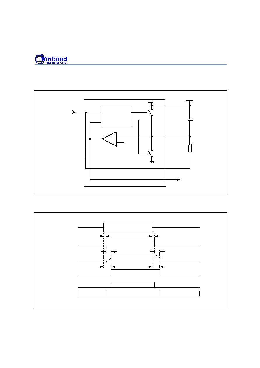
Dual Tone Alert Signal Detection
The dual tone alert signal is separated into high and low tones and detected by a high/low tone
detector. The dual tone alert signal detection circuit is always enabled when the W91030B/BS is not
in sleep state. The ALGR is the output of the dual tone detector and when high indicates that the high
tone and low tone alert signals have been detected. The guard time improves detection performance
by rejecting detected signals with insufficient duration and by masking momentary detection dropout.
Figure 7-4 shows the relationship between the ALGR, ALGRC and ALGO pins and Figure 7-5 shows
the guard time waveform of the same pins. The total recognition time is t
REC
= t
DP
+ t
GP
, where t
DP
is
the tone present detect time and t
GP
is the tone present guard time. The tone present guard time is
the RC time constant with the capacitor discharging from V
SS
to V
DD
( the ALGRC pin discharges
from V
SS
to V
DD
through a resistor). The capacitor will discharge rapidly via a discharge switch after
ALGO returns high. The total absent time is t
ABS
= t
DA
+ t
GA
, where t
DA
is the tone absent detect time
and t
GA
is the tone absent guard time. The tone absent guard time is the RC time constant with the
INP
INN
+
-
GCFB
R1
C1
C2
R2
R4
R3
R5
VREF
Tip
Ring
W91030B
Differential Input Amplifier
C1 = C2
R1 = R2
R3 = (R4 R5) / (R4 +R5)
Voltage Gain
Av = R5 / R1
Input Impedance
Zin = 2 R1
2
+ (1 / wC)
2
0.1 uF
C
R1
R2
Input
+
-
INP
INN
GCFB
VREF
Voltage Gain
V
A
= R2 / R1
W91030B
0.1 uF
Preliminary W91030B
- 8 -
capacitor charging from V
DD
to V
SS
(the ALGRC pin charges from V
DD
to V
SS
through a resistor). The
capacitor will charge rapidly via a charge switch after ALGO returns low. To obtain unequal present
and absent guard times, a diode can be connected as shown in Figure 7-6, to give the unequal
resistance required during capacitor charging and discharging.
Figure 7-4. Guard Time Circuit of Dual Tone Alert Signal Detection
ALGR
ALGRC
ALGO
Discharge
Switch
Charge
Switch
Tip/Ring
ON
ON
ON
Alerting Signal
V
CPth
V
CPth
t
DP
t
GP
t
REC
t
DA
t
GA
t
ABS
Figure 7-5. Guard Time Waveform of ALGR, ALGRC and ALGO pins
Dual tone detected
V
CPth
-
+
Comparator
W91030B
ALGRC
ALGR
ALGO
VDD
VDD
R
C
Discharge
Switch
Charge
Switch
Capacitor
Charge/Discharge
Control Circuit

Preliminary W91030B
Publication Release Date: March 2000
- 9 - Revision A1
Figure 7-6. Guard Time Circuits with Unequal Present and Absent Time
FSK Demodulation
The FSK demodulation circuit is enabled when the FSKE signal is high. An enable time is required to
enable the FSK demodulator circuitry after the FSKE signal goes from low to high.
FSK Carrier Detector
The FSK carrier detector provides an indication of the presence of a signal within the FSK frequency
band. If the output amplitude of the FSK bandpass filter is of sufficient magnitude and holds for 8 mS,
the FSK carrier detect output signal FCDN goes low. FCDN will be released if the FSK bandpass filter
output amplitude is of insufficient magnitude for greater than 8 mS. The 8 mS hysteresis of the FSK
carrier detector is to allow for momentary signal drop out after FCDN has been activated.
When FCDN is inactive, the output of the FSK demodulator is ignored by the FSK data output
interface. In mode 0 of the 3-wire FSK data output interface, DCLK DATA and FDRN are all high and
no clock and no data is driven. In mode 1, the internal shift registers are not updated, and FDRN is
inactive (high state). The DATA is undefined if DCLK is clocked.
3-wire FSK Interface
The 3-wire interface, DCLK, DATA and FDRN pins, form the data interface of the FSK demodulation.
The DCLK pin is the data clock which is either generated by the W91030B or by an external device.
The DATA pin is the serial data pin that outputs data to external devices. The FDRN pin is the data
ready signal, also an output from the W91030B to external devices. There are two modes of this 3-
wire interface that can be selected. Mode 0, where the data transfer is initiated by the W91030B
device, or Mode 1, where the data transfer is initiated by an external microcontroller.
(a) t
GP
> t
GA
t
GP
DD
= R1 C ln [V
DD
CPth
/ (V
-V
)]
t
GA
= R
P
C ln [(V
DD
-V
D
(R
P
/ R2)) / (V
CPth
-V
D
(R
P
/ R2))]
R
P
= R1 R2 / (R1 + R2)
V
D
= diode forward voltage
R1
R2
C
ALGRC
ALR
W91030B
R1
R2
C
ALGRC
ALR
W91030B
(b) t
GP
> t
GA
t
GP
DD
= R1 C ln [V
DD
CPth
/ (V
- V
)]
t
GA
= R
P
C ln [(V
DD
-V
D
(R
P
/ R2)) / (V -V
CPth
-V
D
(R
P
/ R2))]
R
P
= R1 R2 / (R1 + R2)
V
D
= diode forward voltage
DD
V
DD
V
DD

Preliminary W91030B
- 10 -
Mode 0 (MODE = low):
The W91030B processes the FSK signal and outputs signals on the DCLK, DATA and FDRN pins.
Figure 7-7 shows the timing diagram of the 3-wire signals and the input of the FSK signal in mode 0.
For each received stop and start bit sequence, the device outputs a fixed frequency clock string of 8
pulses on the DCLK pin. Each clock rising edge occurs in the middle of each data bit. DCLK is not
generated for the stop and start bits. The DCLK pin is used as a clock driving signal for a serial to
parallel shift register or for a serial data input for a microcontroller. After the 8-bit data has been
shifted out by the device, the FDRN pin will supply a low pulse to inform the microcontroller to
process the 8-bit data.
Tip/Ring
1*
1
0
b0 b1 b2
start
b3 b4 b5 b6 b7 1*
0
b0 b1 b2 b3 b4 b5 b6 b7 1
1
0
b0
stop
start
stop
start
DATA
b0 b1 b2 b3 b4 b5 b6 b7
b0 b1 b2 b3 b4 b5 b6 b7
start
stop
start
stop
start
t
IDD
DCLK
FDRN
1/f
DCLK0
t
CRD
t
RL
1st byte data
2nd byte data
1st byte data
2nd byte data
* Mark bit or redundant stop bit(s), will be omitted.
Figure 7-7. Serial Data Interface Timing of FSK Demodulation in Mode 0
Mode 1 (MODE = high):
The W91030B processes the FSK signal and sets the FDRN pin low to denote the 8-bit boundary and
to indicate to the microcontroller that new data has been transmitted. FDRN will return high on the
first rising edge of DCLK. FDRN is low for half of a nominal bit time (1/2400 sec) if DCLK is not driven
high. DCLK is used to shift 8-bit data out (LSB shift first) on the rising edge. After the last bit (MSB)
has been read, additional clock pulses on DCLK are ignored. Figure 7-8 shows the timing diagram of
the 3-wire signals and the input of the FSK signal in mode 1.

Preliminary W91030B
Publication Release Date: March 2000
- 11 - Revision A1
Demodulated
internal
bit stream
start
0
b0
b1
b2
b3
b4
b5
b6
b7
1
0
stop
stop
start
DATA
b0 b1 b2 b3 b4 b5 b6 b7
DCLK
FDRN
1/f
DCLK1
b7
b6
b5
1
b0
b0
b7
b6
t
DDS
t
DDH
Nth byte data
(N + 1)th byte data
(N - 1)th byte data
Nth byte data
t
RL
Note 2
Note 1
1. FDRN cleared to high by DCLK.
2. FDRN not cleared, low for maximum time (1/2 bit width).
Notes:
Figure 7-8. Serial Data Interface Timing of FSK Demodulation in Mode 1
Other Functions
Interrupt
The interrupt INTN is an open drain output and is used to interrupt the microcontroller. Either RNGON
low, FDRN low or ALGO high will set INTN low and will remain low until all of these three pins return
to an inactive state. The microcontroller must read these pins to know what kind of interrupt occurred
and to make the correct interrupt response.
When the system is powered on, there is no charge on the capacitors. The voltage on the RNGRC pin
is low and RNGON will be low. Also the voltage on the ALGRC pin is high and ALGO will be high if
the SLEEP pin is low. This will cause an interrupt upon power up which will not be cleared until both
capacitors are charged. The microcontroller should therefore ignore the interrupt from these source
until the capacitors are charged up. The microcontroller can examine the RNGON and ALGO pins
and wait until these signals are inactive during a power on interrupt.
It is possible to clear the ALGO pin and its interrupt quickly by setting the SLEEP pin high. In the
sleep mode, the ALGO pin is forced low and the charge switch in Figure 7-4 will turn on, forcing the
capacitor to charge up rapidly.
Sleep Mode
The W91030B can go into a sleep mode by setting SLEEP high, resulting in reduced power
consumption. In this mode, the gain control op-amp, oscillator and all internal circuits, except the ring
detector are disabled. The RNGDI, RNGRC and RNGON pins are not affected, so the device can still
react to call arrival indicators and activate an interrupt to wake up the microcontroller. The sleep
mode can be disabled by the microcontroller.

Preliminary W91030B
- 12 -
Crystal Oscillator
The operation frequency of the W91030B is 3.579545 MHz. Crystal oscillators, ceramic resonators or
other clock sources can be used. A crystal oscillator or ceramic resonator can be directly connected
to the OSCI and OSCO pins without the need for external components. If other clock sources are
used, the OSCI pin should be driven by a clock source and the OSCO pin used to drive other external
clocked devices, or left open. Figure 7-9 shows some applications.
The crystal specification is as follows:
Frequency:
3.579545 MHz
Frequency tolerance:
+/- 0.1 % (-40
�
C to +85
�
C)
Resonance mode:
Parallel
Load capacitance:
18 pF
Maximum series resistance: 150
Maximum drive level (mV): 2 mV
Figure 7-9. Some Application of Clock Driven Circuit
Bias Voltage Generator
The bias voltage generator provides a low impedance voltage source equal to V
DD
/2 and is used to
bias the gain control op-amp. The voltage source is also used for internal circuits. A 0.1
�
F capacitor
had better be placed between the VREF pin and V
SS
to reduce noise.
(a) With crystal osscillator or ceramic resonator
(b) With other clock source
OSCI
OSCO
3.579545 MHz
Oscillator
OSCO
OSCI
OSCO
OSCI
OSCO
W91030B
W91030B
W91030B
OSCI
OSCO
3.579545 MHz
W91030B

Preliminary W91030B
Publication Release Date: March 2000
- 13 - Revision A1
ELECTRICAL CHARACTERISTICS
Absolute Maximum Ratings
(Voltage referenced to V
SS
pin)
PARAMETER
SYMBOL
RATING
UNITS
Supply Voltage with Respect to V
SS
V
DD
-0.3 to 6
V
Voltage on Any Pin Other Than Supplies
(Note 1)
-0.7 to V
DD
+ 0.7
V
Current on Any Pin Other Than Supplies
0 to 10
mA
Storage Temperature
T
st
-65 to 150
�
C
Notes:
1. V
DD
+0.7 should not exceed the maximum rating of the supply voltage.
2. Exposure to conditions beyond those listed under Absolute Maximum Ratings may adversely affect the life and reliability of the
device.
Recommended Operating Conditions
(Voltages referenced to V
SS
)
PARAMETER
SYMBOL
RATING
UNIT
Power Supplies
V
DD
3.0 to 5.5
V
Clock Frequency
F
OSC
3.579545
MHz
Clock Frequency Tolerance
f
C
-0.1 to +0.1
%
Operational Temperature
T
OP
0 to 75
�
C
DC Electrical Characteristics
(V
DD
-
V
SS
= 3.0V. The DC electrical characteristics supersede the recommended operating conditions unless otherwise stated.)
PARAMETER
CONDITION
SYM.
MIN. TYP
MAX. UNITS TEST/
NOTES
Operating Supply Voltage
3.0
5.0
Standby Supply Current
I
DDQ
1
�
A
Test 1
V
DD
= 3.0V
FSKE = High
I
DD1
2.6
3.7
mA
Test 2
Operating Supply Current
V
DD
= 3.0V
FSKE = Low
I
DD2
1.6
2.3
V
DD
= 5.0V
FSKE = High
I
DD1
4.1
5.9
mA
V
DD
= 5.0V
FSKE = Low
I
DD2
2.5
3.6

Preliminary W91030B
- 14 -
DC Electrical Characteristics, continued
PARAMETER
CONDITION SYM.
MIN. TYP
MAX. UNITS TEST/
NOTES
Schmitt Input High Threshold
Schmitt Input Low Threshold
RNGDI,
RNGRC
SLEEP
V
T+
V
T-
0.48
V
DD
0.28
V
DD
0.68
V
DD
0.48
V
DD
V
V
Schmitt Hysteresis
V
HYS
0.2
V
CMOS Input High Voltage
CMOS Input Low Voltage
DCLK, MODE,
FSKE
V
IH
V
IL
0.7 V
DD
V
SS
V
DD
0.3 V
DD
V
Output High Source Current
RGNON,
DCLK, DATA,
FDRN, FCDN,
ALGO,
ALGRC, ALGR
I
OH
0.5
mA
Note 1
Output Low Sink Current
RGNON,
DCLK, DATA,
FDRN, FCDN,
ALGO,
ALGRC,
ALGR, INTN
I
OL
0.5
mA
Note 2
RNGRC
I
OL
2.5
mA
Note 2
Input Current 1
INP, INN,
RNGDI
I
IN
1
1
�
A
Note 3, 5
Input Current 2
SLEEP, DCLK,
MODE, FSKE
I
IN
2
10
�
A
Note 3, 5
Output High-Z Current 1
RNGRC
I
OZ
1
1
�
A
Note
Output High-Z Current 2
ALGRC
I
OZ
2
5
�
A
4, 5
Output High-Z Current 3
INTN
I
OZ
3
10
�
A
Reference Output Voltage
VREF
V
Ref
0.5 V
DD
-4%
0.5 V
DD
+4%
V
Note 6
Reference Output Resistance
VREF
R
Ref
2
K
Comparator Threshold
Voltage
ALGRC
V
CPth
0.5 V
DD
-4%
0.5 V
DD
+4%
V
Tests:
1: All input pins are V
DD
or V
SS
except for oscillator pins, no analog inputs, output unloaded and SLEEP = V
DD
.
2: All input pins are V
DD
or V
SS
except for oscillator pins, no analog inputs, output unloaded, SLEEP = V
SS
and FSKE = V
DD
or
FSKE = V
SS
.
Notes:
"
" Typical figure are at V
DD
= 5V and temperature = 25
�
C are design aids only, not guaranteed and not subject to production
testing.
1. V
OH
= 0.9 V
DD
.
2. V
OL
= 0.1 V
DD
.
3. V
IN
= V
DD
to V
SS
.
4. V
OUT
= V
DD
to V
SS
.
5. Magnitude measurement, ignore signs.
6. Output - no load.

Preliminary W91030B
Publication Release Date: March 2000
- 15 - Revision A1
Electrical Characteristics - Gain Control OP-Amplifier
(Electrical characteristics supersede the recommended operating conditions unless otherwise stated.)
PARAMETER
SYM. MIN. TYP.
MAX. UNITS TEST CONDITIONS
Input Leakage Current
I
IN
1
uA
V
SS
V
IN
V
DD
Input Resistance
R
IN
10
M
Input Offset Voltage
V
OS
25
mV
Power Supply Rejection Ratio
PSRR
40
dB
1 KHz 0.1 Vpp ripple
on V
DD
Maximum Capacitive Load
(GCFB)
C
L
100
pF
Maximum Resistive Load (GCFB)
R
L
50
K
Note: "
" typical figure are at V
DD
= 5V and temperature = 25
�
C are design aids only, not guaranteed and not subject to
production testing.
AC Electrical Characteristics
(AC electrical characteristics supersede the recommended operating conditions unless otherwise stated.)
Dual Tone Alert Signal Detection
PARAMETER
SYM.
MIN.
TYP. MAX. UNITS NOTES
Low Tone Frequency
F
L
2130
Hz
High Tone Frequency
F
H
2750
Hz
Frequency Deviation Acceptance
1.1
%
1
Frequency Deviation Rejection
3.5
%
2
Maximum Input Signal Level
0.22
dBm
a
3
Input Sensitivity Per Tone
-37
-38
dBm
3, 4
Reject Signal Level Per Tone
-45
-44
dBm
3, 4
Positive and Negative Twist
b
Accept
7
dB
Noise Tolerance
SNR
TONE
20
dB
3, 4, 5
Notes:
a. dBm = decibels with a reference power of 1 mW into 600 ohms, 0 dBm = 0.7746 Vrms.
b. Twist = 20 log (F
H
amplitude / F
L
amplitude).
1: The range within which tones are accepted.
2: The range outside of which tones are rejected.
3: These characteristics are for V
DD
= 5V and temperature = 25
�
C.
4: Both tones have the same amplitude. Both tones are at the nominal frequencies.
5: Band limited random noise
300
-
3400 Hz. Present only when the tone is present.

Preliminary W91030B
- 16 -
FSK Detection
PARAMETER
SYMBOL MIN.
TYP.
MAX. UNITS
NOTES
Input Frequency Detection
Bell 202 Mark (logic 1)
Bell 202 Space (logic 0)
CCITT V.23 Mark (logic 1)
CCITT V.23 Space (logic 0)
F
MARK
F
SPACE
F
MARK
F
SPACE
1188
2178
1280.5
2068.5
1200
2200
1300
2100
1212
2222
1319.5
2131.5
Hz
+/-1%
+/-1%
+/-1.5%
+/-1.5%
Maximum Input Signal Level
-5.78
dBm
Input Sensitivity
-43
-45
dBm
1, 2
Transmission Rate
1188
1200
1212
baud
Input Noise Tolerance
SNR
FSK
20
dB
1, 2, 3
Notes:
1. Both mark and space have the same amplitude and are at the nominal frequencies.
2. These characteristics are fort V
DD
= 5V and temperature = 25
�
C.
3. Band limited random noise 300 - 3400 Hz. Present only when the FSK signal is present.
AC Timing Characteristics
(AC timing characteristics supersede the recommended operating conditions unless otherwise stated.)
System
PARAMETER
SYMBOL CONDITION
MIN. TYP.
MAX. UNITS NOTES
Wake-up Time
t
WAKE
SLEEP
50
mS
Sleep-down Time
t
SLP
OSCO
1
mS
Note: "
" typical figures are for V
DD
= 5V and temperature = 25
�
C are design aids only, not guaranteed and not subject to
production testing.
Dual Tone Alert Signal Detection
PARAMETER
SYMBOL CONDITION MIN. TYP.
MAX. UNITS NOTES
Alert Signal Present Detect
Time
t
DP
ALGR
0.5
10
mS
Alert Signal Absent Detect Time
t
DA
0.1
8
mS
Note: "
" typical figure are at V
DD
= 5V and temperature = 25
�
C are design aids only, not guaranteed and not subject to
production testing.
FSK Detection
PARAMETER
SYMBOL CONDITION MIN. TYP.
MAX. UNITS NOTES
FSK Detection Enable Time
t
FSKE
FSKE (high)
25
mS
Input FSK to FCDN Low Delay
t
CP
25
mS

Preliminary W91030B
Publication Release Date: March 2000
- 17 - Revision A1
FSK Detection, continued
PARAMETER
SYMBOL CONDITION MIN. TYP.
MAX. UNITS NOTES
Input FSK to FCDN High Delay
t
CA
FCDN
8
mS
Hysteresis
8
mS
Note: "
" typical figure are at V
DD
= 5V and temperature = 25
�
C are design aids only, not guaranteed and not subject to
production testing.
3-Wire Interface (Mode 0)
PARAMETER
SYMBOL CONDITION MIN. TYP.
MAX. UNITS NOTES
Rise Time
t
RR
200
nS
4
Fall Time
t
RF
FDRN
200
nS
4
Low Time
t
RL
415
416
417
�
S
2
Rate
DATA
1188
1200
1212
bpS
1
Input FSK to DATA Delay
t
IDD
1
5
mS
Rise Time
t
R
200
nS
4
Fall Time
t
F
DCLK
200
nS
4
DATA to DCLK Delay
t
DCD
DATA
6
416
�
S
1, 2, 3
DCLK to DATA Delay
t
CDD
6
416
�
S
1, 2, 3
Frequency
f
DCLK0
1201.6 1202.8
1204
Hz
2
High Time
t
CH
DCLK
415
416
417
�
S
2
Low Time
t
CL
415
416
417
�
S
2
DCLK to FDRN Delay
t
CRD
DCLK, FDRN
415
416
417
�
S
2
Notes:
"
" Ttypical figure are for V
DD
= 5V and temperature = 25
�
C,
are design aids only, not guaranteed and not subject to
production testing.
1. FSK input data rate at 1200 +/-12 baud.
2. OSCI frequency at 3.579545 MHz +/-0.1%.
3. Function of signal condition.
4. 50 pF loading.
3-Wire Interface (Mode 1)
PARAMETER
SYMBOL CONDITION MIN. TYP.
MAX. UNITS NOTES
Frequency
f
DCLK1
1
MHz
Duty Cycle
DCLK
30
70
%
Rise Time
t
R1
20
nS
DCLK Low Set-up to FDRN
t
DDS
DCLK,
500
nS
DCLK Low Hold Time After
FDRN
t
DDH
FDRN
500
nS
Note: "
" typical figure are at V
DD
= 5V and temperature = 25
�
C are design aids only, not guaranteed and not subject to
production testing.

Preliminary W91030B
- 18 -
SLEEP
OSCO
t
WAKE
t
SLP
Figure 8-1. Wake up and Sleep Down Timing
Tip/Ring
ALGR
Alerting Signal
t
DP
t
DA
Alerting Signal
t
DP
t
DA
Figure 8-2. Alert Signal Present and Absent Detect Timing
Tip/Ring
FCDN
Analog FSK Signal
t
CP
t
CA
FSKE
t
FSKE
Analog FSK Signal
t
CP
t
CA
Note
Figure 8-3. FSK Detection Enable and FSK Carrier Detect Present and Absent Timing
Note: The minimal delay from FSKE high to FCDN high is t
FSKE
+ t
CP
, if the analog FSK signal is present before t
FSKE
has
elapsed.
DATA
DCLK
V
HM
V
CT
V
LM
V
HM
V
CT
V
LM
t
CL
t
CH
t
R
t
F
t
DCD
t
CDD
t
R
t
F
V
HM
= 0.7 V , V
CT
= 0.5 V , V
LM
= 0.3 V
DD
DD
DD
Figure 8-4. Data and DCLK Mode 0 Ouput Timing

Preliminary W91030B
Publication Release Date: March 2000
- 19 - Revision A1
FDRN
t
RF
t
RR
t
RL
V
HM
V
CT
V
LM
V
HM
= 0.7 V , V
CT
= 0.5 V , V
LM
= 0.3 V
DD
DD
DD
Figure 8-5. FDRN Output Timing
Tip/Ring
1*
1
0
b0 b1 b2
start
b3 b4 b5 b6 b7 1*
0
b0 b1 b2 b3 b4 b5 b6 b7 1
1
0
b0
stop
start
stop
start
DATA
b0 b1 b2 b3 b4 b5 b6 b7
b0 b1 b2 b3 b4 b5 b6 b7
start
stop
start
stop
start
t
IDD
DCLK
FDRN
1/f
DCLK0
t
CRD
t
RL
1st byte data
1st byte data
2nd byte data
2nd byte data
* Mark bit or redundant stop bit(s), will be omitted.
Figure 8-6. Serial Data Interface Timing of FSK Demodulation in Mode 0
DCLK
t
R1
V
HM
V
LM
V
HM
= 0.7 V , V
DD
LM
= 0.3 V
DD
Figure 8-7. DCLK Mode 1 Input Timing

Preliminary W91030B
- 20 -
Demodulated
internal
bit stream
start
0
b0
b1
b2
b3
b4
b5
b6
b7
1
0
stop
stop
start
DATA
b0 b1 b2 b3 b4 b5 b6 b7
DCLK
FDRN
1/f
DCLK1
b7
b6
b5
1
b0
b0
b7
b6
t
DDS
t
DDH
Nth byte data
(N + 1)th byte data
(N - 1)th byte data
Nth byte data
t
RL
Note 2
Note 1
1. FDRN cleared to high by DCLK.
2. FDRN not cleared, low for maximum time (1/2 bit width).
Notes:
Figure 8-8. Serial Data Interface Timing of FSK Demodulation in Mode 1

Preliminary W91030B
Publication Release Date: March 2000
- 21 - Revision A1
APPLICATION INFORMATION
Application Circuit
Analog Interface
The application circuit of the W91030B in Figure 9-1 shows the device being used within a typical
CPE system. Note that only the circuit between the W91030B and the line interface is shown. The
gain control op-amp is set to unity gain to allow the electrical characteristics to be met in this
application circuit. It should also be noted that if a glitch with sufficient amplitude appears on the tip
and ring interface, this will be detected as a ringing input by this circuit.
Figure 9-1 Application Circuit
Another application circuit for the W91030B, which provides common mode rejection of ringing circuit
signals, is shown in Figure 9-2. When the AC voltage between the tip and ring is greater than the
zener diode breakdown voltage, the photo-coupler LED will turn on, driving RNGDI high and thus
detecting a ringing signal. Note however in this case, a glitch on the tip and ring interface is not able
to turn on the photo-coupler and therefore will not be detected as a ringing signal.
INP
INN
GCFB
VREF
CAP
RNGDI
RNGON
MODE
OSCI
OSCO
VSS
RNGRC
VDD
ALGRC
ALGR
ALGO
INTN
FCDN
FDRN
DATA
DCLK
FSKE
SLEEP/
RESET
TEST
+5V
34K
430K
22nF
Tip/A
+5V
430K
22nF
Ring/B
34K
464K
60K4
+5V
150K
0.22uF
200K
300K
0.1uF
+5V
+5V
0.1uF
R2
R1
+5V
53K6
W91030B
FSK 3-wire interface Mode 0 selected.
Resistor must have 1% tolerance.
Resistor may have 5% tolerance.
Crystal is 3.579545MHz with 0.1% frequency tolerance.
470K
470K
0.1uF
10K
+5V
R1, R2 must calculated according to the formula of Fig. 7-6 (a)
for Bellcore or BT application.
0.1uF
Must rest by
microcontroller
or by RC pulse.
(This net must as short as possible)

Preliminary W91030B
- 22 -
Application Information, continued
Figure 9-2. Application Circuit with Improved Common Mode Noise Immunity
Microcontroller Interface
The following table is the requirement of micorcontroller I/O pin to interface with the W91030B:
CASE RNGON SLEEP FSKE
DCLK
DATA
FDRN
FCDN
INTN
ALGO
1
C
C
C
C
C
C
C
C
C
2
C
C
C
C
C
C
O
C
C
3
C
C
H
C
C
C
O
C
C
4
C
C
H
C
C
O
O
C
C
5
C
C
H
C
C
C
O
O
C
6
C
C
H
C
C
O
O
O
C
7
C
C
H
O
C
O
O
O
C
Note: "C" is connected with microcontroller, "O" is not connected with microcontroller, "H": this pin must set in high state.
INP
INN
GCFB
VREF
CAP
RNGDI
RNGON
MODE
OSCI
OSCO
VSS
RNGRC
VDD
ALGRC
ALGR
ALGO
INTN
FCDN
FDRN
DATA
DCLK
FSKE
SLEEP/
RESET
TEST
+5V
34K
430K
22nF
Tip/A
+5V
430K
22nF
Ring/B
34K
464K
60K4
+5V
150K
0.22uF
+5V
200K
0.01uF
470K
+
-
Vz
0.1uF
0.33uF
12K
+5V
+5V
0.1uF
R2
R1
+5V
53K6
W91030B
FSK 3-wire interface Mode 0 selected.
Resistor must have 1% tolerance.
Resistor may have 5% tolerance.
Crystal is 3.579545MHz with 0.1% frequency tolerance.
R1, R2 must calculated according to the formula of Fig. 7-6 (a)
for Bellcore or BT application.
0.1uF
Must reset by
microcontroller
or by RC pulse.
(This net must as short as

Preliminary W91030B
Publication Release Date: March 2000
- 23 - Revision A1
Case 1: This is the best case for microcontroller to monitor the W91030B, any condition can be
monitored.
Case 2: Analog FSK carrier detect output is not very important, FCDN pin can be ignored.
Case 3: If FSKE pin is not controlled by microcontroller, this pin must set in high state and the FSK
decode circuit is always active when W91030B is not in sleep state. The microcontroller must
take care and ignore the false data when the FSK signal is not expected.
Case 4: The FDRN pin is not very important during FSK decoding if INTN pin is used to interrupt the
microcontroller.
Case 5: If the microcontroller has no interrupt pin to use, any signal occurs of ringing, alert or byte
boundary of FSK data can not notify the microcontroller, the microcontroller must always
monitoring the RNGON, ALGO or FDRN.
Case 6: If FDRN pin can not monitored by microcontroller and the microcontroller has no interrupt pin
to use. In this case, the MODE pin must set low and the W91030B will drive DCLK pin. The
microcontroller must track the timing of DCLK pin, it is a byte boundary if DCLK high for at
least one bit width (1/1200 sec).
Case 7: If FDRN pin and DCLK pin can not monitored by microcontroller and the microcontroller has
no interrupt pin to use. In this case, the MODE pin must set low to set FSK data interface
mode at mode 0 and the microcontroller must track the timing of DATA pin. The DATA pin
will be toggled with 1/1200 second when FSK channel seizure input and stay in high state
when FSK mark signal input, when FSK data input, start bit (low) follows bit 0, bit 1, ...
through bit 7 then at least one bit of stop bit (high). The microcontroller must wait for the start
bit and synchronize it, acquire each bit data at proper time and check the stop bit and then
wait for next start bit arrival. The timer in the microcontroller must reset at the falling edge of
the DATA pin after stop bit has been detected.
Application Environment
There are three major timing differences for caller ID sequences, Bellcore, BT and CCA. Figure 9-3 is
the timing diagram for the Bellcore on-hook data transmission and Figure 9-4 is the timing diagram
for the Bellcore off-hook data transmission. Figure 9-5 is the timing diagram for the BT caller display
service on-hook data transmission and Figure 9-6 is the timing diagram for the BT caller display
service off-hook data transmission. Figure 9-7 is the timing diagram for the CCA caller display service
for on-hook data transmission.

Preliminary W91030B
- 24 -
Tip/Ring
RNGON
SLEEP
FSKE
FCDN
FDRN
DCLK
DATA
1st Ring
Ch. seizure Mark
Message
2nd Ring
A
Note 1
Note 2
...
...101010...
B
C
D
E
F
Data
...
Note 4
Note 3
Note 5
INTN
...
...
Figure 9-3. Input and Output Timing of Bellcore On-hook Data Transmission
A = 2 sec typical
B = 250
-
500 mS
C = 250 mS
D = 150 mS
E = Depends on data length
MAX C + D + E = 2.9 to 3.7 sec
F
200 mS
Notes:
1. The CPE designer may choose to wake up the W91030B only after the end of the RNGON signal to conserve power for a
battery operated CPE. The delay from RNGON to SLEEP (and FSKE) is the reactive time of the microcontroller.
2. The CPE designer may choose to set FSKE to be always high while the CPE is on-hook when the FSK signal is expected.
3. The microcontroller places the W91030B in a sleep condition after the last byte (check sum) has been decoded or FCDN has
become inactive.
4. The W91030B may not be woken up at this ring signal after the FSK data has been processed.
5. If the W91030B has been woken up at the 2nd ring, the microcontroller times out if FCDN is not activated and then puts the
W91030B into a sleep condition.

Preliminary W91030B
Publication Release Date: March 2000
- 25 - Revision A1
Tip/Ring
SLEEP
FSKE
FCDN
FDRN
DCLK
DATA
Note 1
ALGO
CPE unmutes handset
and enables keypad
G
CAS
Note 2
t
REC
t
ABS
A
B
ACK
C
CPE goes off-hook
D
E
F
Mark
Message
Note 5
CPE sends
CPE mutes handset & disables keypad
Note 3
...
Data
Note 4
INTN
...
Figure 9-4. Input and Output Timing of Bellcore Off-hook Data Transmission
A = 75
-
85 mS B = 0
-
100 mS
C = 55
-
65 mS D = 0
-
500 mS
E = 58
-
75 mS F = Depends on data length
G
50 mS
Notes:
1. In a CPE where AC power is not available, the designer may choose to switch over to line power when the CPE goes off-hook and
use battery power while on-hook.
2. The FSKE pin may be set low to prevent the alert tone, speech or other FSK inband noise decoded by FSK demodulator and
give false data when the dual tone alert signal is expected. If the FSKE pin can not controlled by microcontroller, the FSKE pin
must always placed in high state and the microcontroller must give up the FSK decoded data when the FSK signal is not
expected.
3. FSKE should be set high as soon as the CPE has finished sending the acknowledge signal ACK.
4. FSKE may be set low after the last byte (check sum) has been decoded or FCDN has become inactive.
5. For unsuccessful attempts where the end office does not send the FSK signal, the CPE should disable FSKE, unmute the
handset and enable the keypad after this interval has elapsed.

Preliminary W91030B
- 26 -
A/B Wires
RNGON
SLEEP
ALGO
TE DC load
TE AC load
FSKE
FCDN
FDRN
DCLK
DATA
Line Reversal
Alert Signal
Ch. Seizure
Mark
Message
Ring
t
REC
t
ABS
15 1 ms
20 5 ms
A
B
C
D
E
F
G
...
...
...101010...
Data
Note 1
50 - 150 ms
Note 2
Note 3
Note 4
< 120 uA
< 0.5 mA (optional)
Zss (Refer to SIN227)
Current wetting pulse (Refer to SIN227)
INTN
...
...
A >= 100 ms
B = 88 - 110 ms
C >= 45 ms (up to 5 sec)
D = 80 - 262 ms
E = 45 - 75 ms
F <= 2.5 sec (500 ms typical)
G >= 200 ms
Figure 9-5. Input and Output Timing of BT Idle State (On-hook) Data Transmission
Notes:
1. SIN227 specifies that the AC and DC loads should be applied at 20
�
5 mS after the end of the dual tone alert signal.
2. SIN227 specifies that the AC and DC loads should be removed between 50
-
150 mS after the end of the FSK signal.
The W91030B may also be placed in a sleep condition.
3. The FSKE pin should be set low to disable the FSK demodulator when FSK is not expected. The tone alerting signal speech
and the DTMF tones are in the same frequency band as the FSK signal. If the FSKE pin can not controlled by microcontroller, the
FSKE pin must always placed in high state and the microcontroller must give up the FSK decoded data when the FSK signal is
not expected.
4. The W91030B may not be woken up at this ring signal after the FSK data has been processed.

Preliminary W91030B
Publication Release Date: March 2000
- 27 - Revision A1
Tip/Ring
SLEEP
FSKE
FCDN
FDRN
DCLK
DATA
Note 1
ALGO
CPE unmutes handset
and enables keypad
G
Alert Signal
Note 2
t
REC
t
ABS
A
B
ACK
C
CPE goes off-hook
D
E
F
Mark
Message
Note 6
CPE sends
CPE mutes handset & disables keypad
Note 4
...
Data
Note 5
INTN
...
Start Point
Note 3
H
Figure 9-6. Input and Output Timing of BT Loop State (Off-hook) Data Transmission
A = 40
-
50 mS B = 80
-
85 mS
C =
100 mS D = 65
-
75 mS
E = 5
-
100 mS F = 45
-
75 mS
G = Depends on data length H
100 mS
Notes:
1. In a CPE where AC power is not available, the designer may choose to switch over to line power when the CPE goes off-hook and
use battery power while on-hook.
2. The FSKE pin may be set low to prevent the alert tone, speech or other FSK inband noise decoded by FSK demodulator and
give false data when the dual tone alert signal is expected. If the FSKE pin can not controlled by microcontroller, the FSKE pin
must always placed in high state and the microcontroller must give up the FSK decoded data when the FSK signal is not
expected.
3. The exchange will have already disabled the speech path to the distant customer in both transmission directions.
4. The FSKE should be set high as soon as the CPE has finished sending the acknowledge signal ACK.
5. The FSKE may be set low after the last byte (check sum) has been decoded or FCDN has become inactive.
6. In unsuccessful attempts where the exchange does not send the FSK signal, the CPE should disable FSKE, unmute the
handset and enable the keypad after this interval.

Preliminary W91030B
- 28 -
A/B Wires
RNGON
SLEEP
TE DC load
TE AC load
FSKE
FCDN
FDRN
DCLK
DATA
Line Reversal
Ring Burst
Ch. Seizure
Mark
Message
First Ring Cycle
A
B
C
D
E
F
...
...
...101010...
Data
Note 2
Note 3
Note 4
INTN
...
...
A = 200 - 450 mS
B >= 500 mS
C = 80 - 262 mS
D = 45 - 262 mS
E <= 2.5 sec (500 mS typical)
F >= 200 mS
250 - 400 mS
50 - 150 mS
Note 1
Figure 9-7. Input and Output Timing of CCA Caller Display Service Data Transmission
Notes:
1. The CPE designer may choose to set FSKE always high while the the CPE is on-hook and the FSK signal is expected.
2. TW/P & E/312 specifies that the AC and DC loads should be applied between 250
-
400 mS after the end of the ring burst.
3. TW/P & E/312 specifies that the AC and DC loads should be removed between 50
-
150 mS after the end of the FSK signal.
The W91030B may also be placed in a sleep condition.
4. The W91030B may not be woken up at the first ring cycle after the FSK data had been processed.

Preliminary W91030B
Publication Release Date: March 2000
- 29 - Revision A1
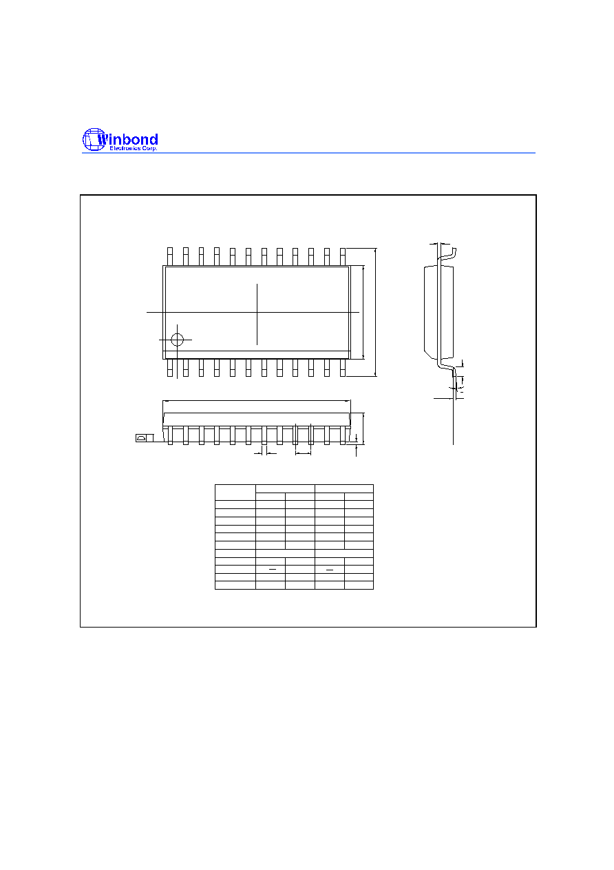
PACKAGE DIMENSIONS
24L PDIP-600mil
Seating Plane
1.63
1.47
0.064
0.058
Symbol
Min.
Nom.
Max.
Max.
Nom.
Min.
Dimension in inches
Dimension in mm
A
B
c
D
e
A
L
S
A
A
1
2
E
0.060
1.52
0.210
5.33
0.010
0.150
0.016
0.155
0.018
0.160
0.022
3.81
0.41
0.25
3.94
0.46
4.06
0.56
0.008
0.120
0.670
0.010
0.130
0.014
0.140
0.20
3.05
0.25
3.30
0.36
3.56
0.555
0.550
0.545
14.10
13.97
13.84
17.02
15.24
14.99
15.49
0.600
0.590
0.610
2.29
2.54
2.79
0.090 0.100 0.110
B
1
1
e
E
1
1.250
1.260
31.75 32.00
0
15
0.085
2.16
0.650
0.630
16.00
16.51
15
0
e
A
2
A
c
E
Base Plane
1
A
1
e
L
A
S
1
E
D
1
B
B
24
13
12
1
�\
�\
Preliminary W91030B
- 30 -
Package Dimensions, continued
24L SOP-300mil
L
O
c
E
H
A1
A
e
b
D
SEATING PLANE
Y
0.25
GAUGE PLANE
E
1
24
13
12
7.60
0.32
0.51
0.30
E
c
b
A1
7.40
0.23
0.33
0.10
0.299
0.013
0.020
0.012
0.291
0.009
0.013
0.004
MAX.
Dimension in mm
2.65
A
SYMBOL
MIN.
2.35
Dimension in Inches
0.104
MIN.
0.093
MAX.
Control demensions are in milmeters.
1.27
0.10
10.65
L
Y
H
0
8
0.40
10.00
e
1.27 BSC
0.050
0.004
0.419
0
0.016
0.394
8
0.050 BSC
E
D
15.20
15.60
0.598
0.614

Preliminary W91030B
Publication Release Date: March 2000
- 31 - Revision A1
Headquarters
No. 4, Creation Rd. III,
Science-Based Industrial Park,
Hsinchu, Taiwan
TEL: 886-3-5770066
FAX: 886-3-5792766
http://www.winbond.com.tw/
Voice & Fax-on-demand: 886-2-27197006
Taipei Office
11F, No. 115, Sec. 3, Min-Sheng East Rd.,
Taipei, Taiwan
TEL: 886-2-27190505
FAX: 886-2-27197502
Winbond Electronics (H.K.) Ltd.
Rm. 803, World Trade Square, Tower II,
123 Hoi Bun Rd., Kwun Tong,
Kowloon, Hong Kong
TEL: 852-27513100
FAX: 852-27552064
Winbond Electronics North America Corp.
Winbond Memory Lab.
Winbond Microelectronics Corp.
Winbond Systems Lab.
2727 N. First Street, San Jose,
CA 95134, U.S.A.
TEL: 408-9436666
FAX: 408-5441798
Note: All data and specifications are subject to change without notice.