Document Outline
- Main Menu
- Video Products
- Search
- Web

W9961CF
H.263/H.261 VIDEO CODEC
- 1 -
W9961CF
H.263/H.261 Video Codec
Version 1.0
April, 1999

W9961CF
- 2 -
Copyright by Winbond Electronics Corp., all rights reserved.
The information in this document has been carefully checked and is believed to be correct as of the
date of publication. Winbond Electronics Corp. reserves the right to make changes in the product or
specification, or both, presented in this publication at any time without notice.
Winbond assumes no responsibility or liability arising from the specification listed herein. Winbond
makes no representations that the use of its products in the manner described in this publication will
not infringe on existing or future patents, trademark, copyright, or rights of third parties. No license is
granted by implication or other under any patent or patent rights of Winbond Electronics Corp.
All other trademarks and registered trademarks are the property of their respective holders.

W9961CF
- 3 -
TABLE OF CONTENTS
1 GENERAL DESCRIPTION..................................................................................................................... 7
2 FEATURES............................................................................................................................................... 8
3 PIN CONFIGURATION ........................................................................................................................ 10
4 PIN DESCRIPTION ............................................................................................................................... 11
4.1 P
IN
D
EFINITION
........................................................................................................................................ 11
4.2 P
IN
L
IST
................................................................................................................................................... 17
4.3 P
OWER
O
N
R
ESET
I
NITIALIZATION
............................................................................................................. 22
5 SYSTEM DIAGRAM ............................................................................................................................. 24
6 BLOCK DIAGRAM ............................................................................................................................... 26
7 FUNCTIONAL DESCRIPTION ............................................................................................................ 27
7.1 VPRE P
ROCESSOR
.................................................................................................................................... 27
7.2 V
IDEO
C
ODEC
........................................................................................................................................... 28
7.2.1 Video Coding .................................................................................................................................... 28
7.2.1.1 I-pictures INTRA Coding .............................................................................................................................28
7.2.1.2 P-pictures INTER Coding ............................................................................................................................29
7.2.1.3 P-pictures INTRA Coding ............................................................................................................................29
7.2.2 Video Decoding ................................................................................................................................ 29
7.3 VPOST P
ROCESSOR
................................................................................................................................. 30
7.3.1 Video Post-processing....................................................................................................................... 30
7.3.2 Display Control ................................................................................................................................ 31
7.3.3 Video Output Control........................................................................................................................ 31
7.3.3.1 Hue, Saturation, Contrast, and Brightness Adjustments................................................................................31
7.3.3.2 Video Output Interface.................................................................................................................................32
7.4 RISC M
ICROPROCESSOR
........................................................................................................................... 35
7.4.1 RISC Pipeline Stages ........................................................................................................................ 35
7.4.2 Address Spaces ................................................................................................................................. 36
7.4.2.1 Program Memory Address Space..................................................................................................................36
7.4.2.2 Data Memory Address Space .......................................................................................................................36
7.4.3 RISC Registers .................................................................................................................................. 38
7.4.3.1 General Registers ........................................................................................................................................38
7.4.3.2 Shadow Registers ........................................................................................................................................38
7.4.4 RISC Interrupt Handling ................................................................................................................... 39
7.5 INTC (I
NTERRUPT
C
ONTROLLER
).............................................................................................................. 41
7.6 T
IMER
...................................................................................................................................................... 43
7.7 FDMA C
ONTROLLER
................................................................................................................................ 44
7.7.1 FDMA Transfer Modes ..................................................................................................................... 45
7.7.2 FDMA Transfer Types....................................................................................................................... 45

W9961CF
- 4 -
7.7.3 FDMA Programming ........................................................................................................................ 45
7.8 H
OST
I
NTERFACE
C
ONTROLLER
................................................................................................................. 48
7.8.1 PCI Address Spaces .......................................................................................................................... 48
7.8.2 PCI Interrupt Control ....................................................................................................................... 48
7.9 DRAM C
ONTROLLER
............................................................................................................................... 50
7.9.1 Video Memory Arbitration ................................................................................................................ 50
7.9.2 DRAM Interface................................................................................................................................ 51
7.10 ISA-
LIKE
B
US
I
NTERFACE AND
GPIO
S
..................................................................................................... 52
7.10.1 ISA-like Bus Interface ..................................................................................................................... 52
7.10.2 GPIO .............................................................................................................................................. 52
7.11 PLL (P
HASE
L
OCKED
L
OOP
).................................................................................................................... 53
8 ELECTRICAL CHARACTERISTICS .................................................................................................. 54
8.1 A
BSOLUTE
M
AXIMUM
R
ATINGS
................................................................................................................. 54
8.2 DC C
HARACTERISTICS
.............................................................................................................................. 54
8.2.1 DAC DC Characteristics................................................................................................................... 54
8.2.2 Digital DC Characteristics ............................................................................................................... 58
8.3 AC C
HARACTERISTICS
.............................................................................................................................. 59
8.3.1 DAC AC Characteristics ................................................................................................................... 59
8.3.2 PLL AC Characteristics .................................................................................................................... 59
8.3.3 RESET Timing AC Characteristics.................................................................................................... 60
8.3.4 Clock AC Characteristics.................................................................................................................. 60
8.3.5 Input Timing AC Characteristics....................................................................................................... 61
8.3.6 Output Timing AC Characteristics .................................................................................................... 62
9 PACKAGE SPEC. .................................................................................................................................. 64
10 ORDERING INFORMATION............................................................................................................. 65

W9961CF
- 5 -
LIST OF FIGURES
F
IGURE
3.1 W9961CF P
IN
C
ONFIGURATION
.................................................................................................... 10
F
IGURE
5.1 W9961CF-B
ASED
S
TAND
-
ALONE
V
IDEOPHONE
S
YSTEM
D
IAGRAM
................................................. 24
F
IGURE
6.1 W9961CF B
LOCK
D
IAGRAM
......................................................................................................... 26
F
IGURE
7.1 VPRE P
ROCESSOR
B
LOCK
D
IAGRAM
............................................................................................. 27
F
IGURE
7.2 V
IDEO
C
ODEC
B
LOCK
D
IAGRAM
.................................................................................................... 28
F
IGURE
7.3 VPOST P
ROCESSOR
B
LOCK
D
IAGRAM
........................................................................................... 30
F
IGURE
7.4 T
YPICAL
T
HREE
-
WINDOW
D
ISPLAY FOR
V
IDEO
C
ONFERENCING
A
PPLICATIONS
................................ 31
F
IGURE
7.5 H
UE
, S
ATURATION
, C
ONTRAST
,
AND
B
RIGHTNESS
C
ONTROLS
........................................................ 32
F
IGURE
7.6 RISC M
ICROPROCESSOR
B
LOCK
D
IAGRAM
.................................................................................... 35
F
IGURE
7.7 P
ROGRAM
M
EMORY
A
DDRESS
S
PACE
............................................................................................. 37
F
IGURE
7.8 D
ATA
M
EMORY
A
DDRESS
S
PACE
................................................................................................... 37
F
IGURE
7.9 RISC G
ENERAL
R
EGISTERS
........................................................................................................... 38
F
IGURE
7.10 INTC B
LOCK
D
IAGRAM
.............................................................................................................. 41
F
IGURE
7.11 T
IMER
B
LOCK
D
IAGRAM
.............................................................................................................. 43
F
IGURE
7.12 FDMA C
ONTROLLER
B
LOCK
D
IAGRAM
....................................................................................... 44
F
IGURE
7.13 B
LOCK
T
RANSFER
M
ODE WITH
B
LOCK
A
DDRESSING
..................................................................... 46
F
IGURE
7.14 D
EMAND
T
RANSFER
M
ODE WITH
L
INEAR
A
DDRESSING
................................................................. 47
F
IGURE
7.15 H
OST
I
NTERFACE
C
ONTROLLER
B
LOCK
D
IAGRAM
........................................................................ 48
F
IGURE
7.16 DRAM C
ONTROLLER
B
LOCK
D
IAGRAM
....................................................................................... 50
F
IGURE
7.17 PLL B
LOCK
D
IAGRAM
................................................................................................................. 53
F
IGURE
8.1 525-
LINE
(NTSC/PAL-M) Y (L
UMINANCE
) O
UTPUT
W
AVEFORM
................................................... 55
F
IGURE
8.2 625-
LINE
(PAL-B, D, G, H, N) Y (L
UMINANCE
) O
UTPUT
W
AVEFORM
............................................ 55
F
IGURE
8.3 525-
LINE
(NTSC/PAL-M) C (C
HROMINANCE
) O
UTPUT
W
AVEFORM
.............................................. 56
F
IGURE
8.4 625-
LINE
(PAL-B, D, G, H, N) C (C
HROMINANCE
) O
UTPUT
W
AVEFORM
....................................... 56
F
IGURE
8.5 525-
LINE
(NTSC/PAL-M) C
OMPOSITE
V
IDEO
O
UTPUT
W
AVEFORM
............................................... 57
F
IGURE
8.6 625-
LINE
(PAL-B, D, G, H, N) C
OMPOSITE
V
IDEO
O
UTPUT
W
AVEFORM
........................................ 57
F
IGURE
8.7 RESET T
IMING
............................................................................................................................ 60
F
IGURE
8.8 C
LOCK
W
AVEFORM
....................................................................................................................... 60
F
IGURE
8.9 I
NPUT
T
IMING
............................................................................................................................... 61
F
IGURE
8.10 O
UTPUT
T
IMING
.......................................................................................................................... 62
F
IGURE
9.1 208L QFP (28X28
MM FOOTPRINT
2.6
MM
) D
IMENSIONS
................................................................ 64

W9961CF
- 6 -
LIST OF TABLES
T
ABLE
4.1 W9961CF P
IN
L
IST
........................................................................................................................ 17
T
ABLE
4.2 W9961CF P
OWER
O
N
R
ESET
D
EFINITIONS
..................................................................................... 22
T
ABLE
7.1 W9961CF V
IDEO
O
UTPUT
M
ODES
................................................................................................. 32
T
ABLE
7.2 W9961CF V
IDEO
O
UTPUT
I
NTERFACE
P
IN
A
SSIGNMENT
................................................................. 34
T
ABLE
7.3 D
ATA
M
EMORY
A
DDRESS
M
APPING
................................................................................................ 37
T
ABLE
7.4 RISC I
NTERRUPT
V
ECTORS
............................................................................................................ 39
T
ABLE
7.5 I
NTERRUPT
C
HANNELS
................................................................................................................... 41
T
ABLE
7.6 FDMA C
HANNELS
......................................................................................................................... 44
T
ABLE
7.7 PCI I
NTERRUPT
C
HANNELS
............................................................................................................ 48
T
ABLE
7.8 SDRAM
AND
EDO DRAM I
NTERFACE
S
IGNALS
............................................................................ 51
T
ABLE
7.9 ISA-
LIKE
B
US
A
CCESS
M
ODES
........................................................................................................ 52
T
ABLE
8.1 A
BSOLUTE
M
AXIMUM
R
ATINGS
....................................................................................................... 54
T
ABLE
8.2 DAC DC C
HARACTERISTICS
........................................................................................................... 54
T
ABLE
8.3 D
IGITAL
DC C
HARACTERISTICS
....................................................................................................... 58
T
ABLE
8.4 DAC AC C
HARACTERISTICS
........................................................................................................... 59
T
ABLE
8.5 TV M
ODES
R
ESOLUTION AND
C
LOCK
R
ATE
..................................................................................... 59
T
ABLE
8.6 PLL AC C
HARACTERISTICS
............................................................................................................ 59
T
ABLE
8.7 RESET T
IMING
.............................................................................................................................. 60
T
ABLE
8.8 C
LOCK
AC C
HARACTERISTICS
......................................................................................................... 60
T
ABLE
8.9 PCICLK-R
EFERENCED
I
NPUT
T
IMING
AC C
HARACTERISTICS
........................................................... 61
T
ABLE
8.10 SMCLK-R
EFERENCED
I
NPUT
T
IMING
AC C
HARACTERISTICS
.......................................................... 61
T
ABLE
8.11 VICLK-R
EFERENCED
I
NPUT
T
IMING
AC C
HARACTERISTICS
........................................................... 62
T
ABLE
8.12 PCICLK-R
EFERENCED
O
UTPUT
T
IMING
AC C
HARACTERISTICS
...................................................... 62
T
ABLE
8.13 SMCLK-R
EFERENCED
O
UTPUT
T
IMING
AC C
HARACTERISTICS
...................................................... 62
T
ABLE
8.14 PCLK-R
EFERENCED
O
UTPUT
T
IMING
AC
C
HARACTERISTICS
.......................................................... 63

W9961CF
- 7 -
1 GENERAL DESCRIPTION
The W9961CF is a highly integrated single chip video codec provided by Winbond Electronics Corp.
The W9961CF performs video compression and decompression fully compliant with ITU-T H.263 and
H.261 standards for video conferencing. Working in conjunction with the high performance 32-bit
RISC, W90220CF, the W9961CF is aimed to provide a complete video solution that supports both
the H.324 international standard for video conferencing over regular telephone lines (Public Switched
Telephone Network, or PSTN) as well as the H.320 international standard for ISDN video
conferencing. Moreover, the W9961CF integrates a high quality NTSC/PAL TV encoder to directly
interface to TV or LCD, eliminating the need for a separate TV encoder for stand-alone or set-top
videophone.
To achieve high performance video coding and decoding, many hardware engines are integrated in
the W9961CF, which perform Motion Estimation and Motion Compensation, Discrete Cosine
Transform (DCT) and Inverse Discrete Cosine Transform (IDCT), Quatization and Inverse
Quantization, Zig-zag Scan, Variable Length Encoding and Variable Length Decoding (VLD), etc. A
high performance 16-bit RISC with 5Kx22 bits program memory (PM) and 1Kx16 bits data memory
(DM) is also integrated for H.263/H.261 coding/decoding control and intelligent frame rate control.
There are three picture formats supported by the W9961 encoder and decoder: sub-QCIF, QCIF, and
CIF. The W9961CF, when operated at 70 Mhz clock frequency, is capable to encode/decode sub-
QCIF, QCIF, or CIF at 30 fps.
The W9961CF can accept NTSC or PAL video, square, or rectangular pixels, and convert to sub-
QCIF, QCIF, or CIF format. A two-dimensional noise reduction filter is integrated to reduce noise and
improve coding efficiency. Built-in cropping window control and arbitrary scaling in both the horizontal
and vertical directions can serve as the digital pan and zoom over a user-specified region for camera
control.
In the video post-processing, the W9961CF supports two movable and arbitrarily scaleable windows
with picture-in-picture (PIP) feature for remote and local view video. A built-in post deblocking filter is
used to reduce visible artifacts of remote view from video compression. The local view video can be
mirrored or unmirrored. A display controller is built-in with 4-/8-/16-bit color modes for background or
on-screen-display (OSD). A high quality NTSC/PAL TV encoder is also integrated to directly interface
to TV or LCD.
An on-chip DRAM controller is used to interface to SDRAM or EDO DRAM through 32-bit data bus.
The W9961CF is a 3.3 V device with TTL-compatible 3.3 V or 5.0 V I/O, and is packaged in 208-pin
PQFP.

W9961CF
- 8 -
2 FEATURES
Video Codec
�
Fully compliant with ITU-T international standards H.263 and H.261
�
Encodes/decodes in sub-QCIF (128x96), QCIF (176x144), or CIF (352x288) picture format
�
Encodes/decodes sub-QCIF/QCIF/CIF at 30 frames per second (fps)
�
Supports both integer search and half-pixel search motion estimation
�
Supports several H.263 Version 2 preferred modes including
Annex D
Unrestricted Motion Vectors (With UUI = 1)
Annex J
Deblocking Filter
Annex K
Slice Structured Mode
Annex L
Supplemental Enhancement Information (Full-Frame Freeze Only)
Annex T
Modified Quantization
Video Pre-processing
�
Direct connect to digital camera through 8- or 16-bit data bus
�
Glueless interface to NTSC/PAL TV decoder
�
Input video format compliant with YCbCr 4:2:2 CCIR 601 standard
�
Built-in two-dimensional noise reduction filter to reduce noise and improve coding efficiency
�
Built-in cropping and arbitrary scaling for digital pan and zoom camera control
Video Post-processing
�
Built-in two moveable and arbitrarily scalable video windows with picture-in-picture (PIP)
�
Built-in post deblocking filter to reduce visible artifacts of remote view from video compression
�
The local view can be mirrored or unmirrored
�
Built-in display controller with 4-/8-/16-bit color modes for background or on-screen-display (OSD)
�
Built-in NTSC/PAL TV encoder with three 9-bit DACs for direct TV output
�
Built-in 3-line 1D/2D flicker-free filter for best text quality
�
Supports three composite video, one S-Video and one composite video, or one RGB output

W9961CF
- 9 -
�
Hue, saturation, contrast, and brightness adjustments
ISA-like Interface and GPIOs
�
Direct connect to DSPG CT802X-series audio processor through 8-bit ISA-like interface
�
Provides several general purpose I/O ports which can be configured as serial ports, keypad
control, button control, remote control, etc.
Host Interface
�
Direct connect to Winbond W902X0-series CPU through 32-bit PCI bus
�
PCI 2.1 compliant
Memory Interface
�
Supports SDRAM or 1-cycle EDO DRAM at 70 Mhz maximum clock frequency
�
Supports 32-bit DRAM interface in 1, 2 or 4 Mbytes configuration
Built-in Programmable Phase-Locked Loop (PLL) Clock Synthesizer
Operating Frequency is 70 Mhz with Video Input Frequency of 13.5 MHz (typical), Video
Output Frequency of 27.0 Mhz, and PCI Clock Frequency of 33 MHz
3.3 V Device with TTL-compatible 3.3 V or 5.0 V I/O
Fabricated in Advanced 0.35um TLM Technology
208L QFP Package

W9961CF
- 10 -
3 PIN CONFIGURATION
The W9961CF is packaged in a 208L QFP. The pin configuration is shown in Figure 3.1.
W9961CF
(Top View)
MA0
V
D
D
5
V
55
1
0
A
D
3
1
A
D
3
0
V
S
S
B
M
D
2
3
V
D
D
B
P
3
Y
4
P
2
Y
5
G
P
I
O
4
U
V
0
U
V
1
D
E
M
M
D
2
0
M
D
1
9
M
D
2
1
M
D
2
4
M
D
2
5
M
D
2
6
M
D
2
2
M
D
2
7
M
D
2
8
M
D
2
9
M
D
3
0
M
D
3
1
V
S
S
B
G
P
I
O
0
G
P
I
O
1
G
P
I
O
2
V
D
D
I
G
P
I
O
3
V
S
S
I
U
V
2
U
V
3
U
V
4
U
V
5
U
V
6
U
V
7
Y
1
V
D
D
B
Y
0
Y
2
Y
3
Y
6
Y
7
V
S
H
S
V
I
C
L
K
V
S
S
B
P
0
P
1
H
S
Y
N
C
V
S
S
B
A
D
2
9
A
D
2
8
V
D
D
B
A
D
2
7
A
D
2
6
A
D
2
5
A
D
2
4
C
/
B
E
3
#
I
D
S
E
L
A
D
2
3
A
D
2
2
A
D
2
1
A
D
2
0
A
D
1
9
A
D
1
8
A
D
1
7
A
D
1
6
V
D
D
I
C
/
B
E
2
#
F
R
A
M
E
#
V
S
S
I
I
R
D
Y
#
T
R
D
Y
#
V
S
S
B
D
E
V
S
E
L
#
S
T
O
P
#
V
D
D
B
P
E
R
R
#
S
E
R
R
#
P
A
R
C
/
B
E
1
#
A
D
1
5
A
D
1
4
A
D
1
3
A
D
1
2
A
D
1
1
A
D
1
0
A
D
9
A
D
8
V
S
S
B
C
/
B
E
0
#
A
D
7
A
D
6
A
D
5
A
D
4
A
D
3
A
D
2
A
D
1
A
D
0
V
S
Y
N
C
5
1
2
0
1
5
2
5
3
0
3
5
4
0
4
5
5
0
1
0
5
1
1
0
1
1
5
1
2
0
1
2
5
1
3
0
1
3
5
1
4
0
1
4
5
1
5
0
1
5
5
60
65
70
75
80
85
90
95
100
205
200
195
190
185
180
175
170
165
160
MA1
MA2
MA3
MA4
VSSB
MA5
MA6
VDDB
MA7
MA8
MA9
MA10
BA
VSSB
SMCLK
VSSI
SCAS#
VDDI
SRAS#
OE#/CKE
WE#
CAS0#/DQM0
CAS1#/DQM1
VSSB
RAS0#/CS0#
MD0
MD1
MD2
VDDB
MD3
MD4
MD5
MD6
MD7
MD8
MD9
VSSB
MD10
MD11
MD12
MD13
MD14
MD15
CAS2#/DQM2
CAS3#/DQM3
VDDB
RAS1#/CS1#
VSSB
MD16
MD17
MD18
P5
P4
P7
P6
VDDI
PCLK
CP1/Y/G
CP2/C/B
VREF
CP0/R
EXTVREF
RSET
COMP
DACAVSS
VDD5V
DACAVDD
SD1
SD0
SD3
SD2
SD4
VSSB
SD6
SD5
VOCLK
SD7
SA1
SA0
SA2
VSSI
VDDB
SA3
SA5
SA4
SA6
VSSB
SA8
SA7
SA10
SA9
SA12
SA11
SRD#
EINT#
PLLAVDD
SWR#
MCLK
PLLAVSS
INTA#
VOCLK/2
PCICLK
RST#
Figure 3.1 W9961CF Pin Configuration

W9961CF
- 11 -
4 PIN DESCRIPTION
The following tables provide a brief description of each pin on the W9961CF. The following signal
type definitions are used in these descriptions:
I
Input pin
IU
Input pin with internal pull-up resistor
B
Bi-directional input/output pin
O
Output pin
TS
Tri-State output pin
STS
Sustained Tri-State pin. Must drive it high for at least one PCI clock before letting it float.
A
Analog pin
P
Power supply pin
G
Ground pin
#
Active low
4.1 Pin Definition
PCI Bus Interface (48 pins)
Pin Name
Pin Number
Type
Description
AD[31:0]
1, 2, 4, 5, 7-
10, 13-20,
35-42, 45-52
B
Multiplexed System Address and Data Bus. The address phase
is the clock cycle in which FRAME# is asserted. Data is
transferred during those clocks where both IRDY# and TRDY#
are asserted.
C/BE[3:0]#
11, 22, 34, 44
I
Multiplexed Bus Command and Byte Enables. During the
address phase of a transaction, C/BE[3:0]# define the bus
command. During the data phase C/BE[3:0]# are used as Byte
Enables.
PAR
33
TS
Parity. It is even parity across AD31-AD0 and C/BE[3:0]#.
FRAME#
23
I
Cycle Frame. Asserted to indicate a bus transaction is
beginning.
TRDY#
26
STS
Target Ready. A data phase is completed on any clock both
TRDY# and IRDY# are sampled asserted.
IRDY#
25
I
Initiator Ready. A data phase is completed on any clock both
IRDY# and TRDY# are sampled asserted.

W9961CF
- 12 -
INTA#
206
TS
Interrupt Request. Asserted low, level sensitive.
STOP#
29
STS
Stop. Asserted to request the master to stop the current
transaction.
DEVSEL#
28
STS
Device Select. Asserted to indicate the W9961CF has decoded
its address as the target of the current access.
IDSEL
12
I
Initialization Device Select. Used as chip select during
configuration read and write transactions.
PERR#
31
STS
Parity Error. It is only for the reporting of data parity errors
during the PCI transactions. The W9961CF cannot report a
PERR# until it has claimed the access by asserting DEVSEL#
and completed a data phase.
SERR#
32
TS
System Error. It is for reporting address parity errors, or any
other system error where the result will be catastrophic.
PCICLK
208
I
PCI System Clock. Up to 33 Mhz for W9961CF.
RST#
207
I
System Reset.
Video Memory Interface (55 pins)
Pin Name
Pin Number
Type
Description
MD[31:0]
120-115,113-
109, 107, 106,
104-102, 96-
91, 89-83, 81-
79
B
Data Bus.
Note: MD[15:0] are also used as the system configuration
strapping bits, providing system configuration and setup
information upon power-on or reset.
MA[10:0]
65-62, 60, 59,
57-53
O
Address Bus.
Note: for SDRAM, MA[10:0] are sampled during the ACTIVE
command (row address MA[10:0]) and READ/WRITE command
(column address MA[7:0], with MA10 defining AUTO
PRECHARGE) to select one location out of the 512K available
in the respective bank. MA10 is sampled during a
PRECHARGE command to determine if all banks are to be
precharged (MA10 HIGH).
RAS[1:0]#
CS[1:0]#
100, 78
O
EDO DRAM: Row Address Strobes.
SDRAM: Chip Select. CS[1:0]# enable the command decoder

W9961CF
- 13 -
for each external memory bank.
CAS[3:0]#
DQM[3:0]
98, 97, 76, 75
O
EDO DRAM: Column Address Strobes.
SDRAM: Input/Output Mask. DQM[3:0] are input mask signals
for write accesses and output enable signals for read accesses.
DQM0 corresponds to MD[7:0]; DQM1 corresponds to
MD[15:8]; DQM2 corresponds to MD[23:16]; DQM3
corresponds to MD[31:24].
OE#
CKE
73
O
EDO DRAM: Output Enable.
SDRAM: Clock Enable. CKE activates the SMCLK signal. The
SDRAM enters precharge power-down to deactivate the input
and output buffers, excluding CKE, for maximum power saving
when CKE is LOW coincident with a NOP.
WE#
74
O
EDO DRAM: Write Enable.
SDRAM: Command Input. SRAS#, SCAS#, and WE# (along
with CS#) define the command being entered.
SRAS#
72
O
EDO DRAM: Not used.
SDRAM: Command Input. SRAS#, SCAS#, and WE# (along
with CS#) define the command being entered.
SCAS#
70
O
EDO DRAM: Not used.
SDRAM: Command Input. SRAS#, SCAS#, and WE# (along
with CS#) define the command being entered.
BA
66
O
EDO DRAM: Not used.
SDRAM: Bank Address Input. BA defines to which internal bank
the ACTIVE, READ, WRITE or PRECHARGE command is
being applied. BA is also used to program the 12th bit of the
Mode Register.
SMCLK
68
O
EDO DRAM: Not used.
SDRAM: Clock.
Input Video Interface (19 pins)
Pin Name
Pin Number
Type
Description

W9961CF
- 14 -
Y[7:0]
146-139
I
Digital Y (Luminance) Inputs in 16-bit Mode, or Digital YUV
Inputs in 8-bit Mode.
UV[7:0]
137-130
IU
Digital UV (Chrominance) Inputs in 16-bit Mode, or Not Used in
8-bit Mode.
HS
148
I
Horizontal Sync. Input. Programmable polarity.
VS
147
I
Vertical Sync Input. Programmable polarity.
VICLK
149
I
Input Video Clock.
Output Video Interface (20 pins)
Pin Name
Pin Number
Type
Description
CP2
C
B
163
O
Composite Video Mode: Composite Video Output.
S-Video + Composite Video Mode: Chrominance Output.
RGB Output Mode: Blue Video Output.
CP1
Y
G
164
O
Composite Video Mode: Composite Video Output.
S-Video + Composite Video Mode: Luminance Output.
RGB Output Mode: Green Video Output.
CP0
R
165
O
Composite Video Mode: Composite Video Output.
S-Video + Composite Video Mode: Composite Video Output.
RGB Output Mode: Red Video Output.
P[7:0]
151-154, 157-
160
B
8-bit YCbCr Mode: Digital YCbCr Video Output Data.
8-bit RGB Mode: Digital RGB Video Output Data.
PCLK
161
TS
8-bit YCbCr Mode: 2
� Pixel Clock Output.
8-bit RGB Mode:
2
3
�
Pixel Clock Output.
HSYNC
155
TS
Horizontal Sync.

W9961CF
- 15 -
VSYNC
156
TS
Vertical Sync.
DEM
128
B
Data Enable control signal for LCD interface.
VREF
166
A
Voltage Reference. A 0.1uF bypass capacitor should always be
connected between this pin and TVAVDD, with short leads and
in close proximity to the device pins.
RSET
167
A
Reference Resistor. A resistor should be connected from this
pin to TVAVSS to control the full-scale current value.
EXTVREF
168
A
External VREF Mode: External Voltage Reference (analog
input). An external voltage reference must supply this pin with a
1.235 V (typical) reference. A 0.1uF bypass capacitor should
always be connected between this pin and TVAVDD.
Internal VREF Mode: A 0.1uF bypass capacitor should always
be connected between this pin and TVAVDD.
COMP
170
A
Compensation Pin. A 0.1uF bypass capacitor should always be
connected between this pin and TVAVDD, with short leads and
in close proximity to the device pins.
VOCLK
182
I
Output Video Clock. A stable 27 MHz reference clock input.
ISA-like Bus Interface and GPIO Ports (29 pins)
Pin Name
Pin Number
Type
Description
SD[7:0]
181-178, 176-
174, 172
B
Data Bus. ISA-like data bus to interface with the Audio
Processor.
SA[12:0]
198-192, 190,
189, 187, 186,
184, 183
B
Address Bus. They are output pins in normal operation
(PWON_14-12 = 111), while serve as address inputs when in
the Internal RAM/ROM Test mode (PWON_14-12
111).
SWR#
201
B
I/O Write. It is output pin in normal operation (PWON_14-12 =
111), while serves as write input when in the Internal RAM/ROM
Test mode (PWON_14-12
111).
SRD#
200
B
I/O Read. It is output pin in normal operation (PWON_14-12 =
111), while serves as read input when in the Internal RAM/ROM
Test mode (PWON_14-12
111).
EINT#
199
IU
Interrupt Request Input.
W9961CF
- 16 -
GPIO[4:0]
122-125, 127
B
General Purpose Input/Out Ports. With internal pull-up resistor.
Clock Interface (2 pins)
Pin Name
Pin Number
Type
Description
VOCLK/2
205
TS
VOCLK By 2. A Stable 13.5 MHz clock output.
MCLK
204
IU
External MCLK Mode: Main Clock Input.
Internal MCLK Mode: Not used.
Power and Ground (35 pins)
Pin Name
Pin Number
Type
Description
VDDB
6, 30, 61, 82,
99, 114, 138,
188
P
Buffer Power Supply. Provides isolated power to the input and
output buffers for improved noise immunity. +3.3 V
� 0.3 V.
VDD5V
105, 173
P
5V Buffer Power Supply. Provides 5V power to the input and
output buffers for 5V input tolerance. +5.0 V
� 0.25 V.
VSSB
3, 27, 43, 58,
67, 77, 90,
101, 108, 121,
150, 177, 191
G
Buffer Ground.
VDDI
21, 71, 126,
162
P
Core Power Supply. +3.3 V
� 0.3 V.
VSSI
24, 69, 129,
185
G
Core Ground.
DACAVDD
171
P
DAC Analog Power Supply. Provides isolated power to the DAC
analog ckts for improved noise immunity. +3.3 V
� 0.3 V.
DACAVSS
169
G
DAC Analog Ground.
PLLAVDD
202
P
PLL Analog Power Supply. Provides isolated power to the PLL
analog ckts for improved noise immunity. +3.3 V
� 0.3 V.
PLLAVSS
203
G
PLL Analog Ground.

W9961CF
- 17 -
4.2 Pin List
Table 4.1 W9961CF Pin List
Number
Name
Type
Pull-up
IOH (mA)
IOL (mA)
Load (pf)
1
AD31
B
-3
8
50
2
AD30
B
-3
8
50
3
VSSB
G
4
AD29
B
-3
8
50
5
AD28
B
-3
8
50
6
VDDB
P
7
AD27
B
-3
8
50
8
AD26
B
-3
8
50
9
AD25
B
-3
8
50
10
AD24
B
-3
8
50
11
C/BE3#
I
12
IDSEL
I
13
AD23
B
-3
8
50
14
AD22
B
-3
8
50
15
AD21
B
-3
8
50
16
AD20
B
-3
8
50
17
AD19
B
-3
8
50
18
AD18
B
-3
8
50
19
AD17
B
-3
8
50
20
AD16
B
-3
8
50
21
VDDI
P
22
C/BE2#
I
23
FRAME#
I
24
VSSI
G
25
IRDY#
I
26
TRDY#
STS
-3
8
50
27
VSSB
G
28
DEVSEL#
STS
-3
8
50
29
STOP#
STS
-3
8
50
30
VDDB
P
31
PEER#
STS
-3
8
50
32
SERR#
TS
-2
4
50
33
PAR
TS
-3
8
50
34
C/BE1#
I
35
AD15
B
-3
8
50
36
AD14
B
-3
8
50
37
AD13
B
-3
8
50

W9961CF
- 18 -
38
AD12
B
-3
8
50
39
AD11
B
-3
8
50
40
AD10
B
-3
8
50
41
AD9
B
-3
8
50
42
AD8
B
-3
8
50
43
VSSB
G
44
C/BE0#
I
45
AD7
B
-3
8
50
46
AD6
B
-3
8
50
47
AD5
B
-3
8
50
48
AD4
B
-3
8
50
49
AD3
B
-3
8
50
50
AD2
B
-3
8
50
51
AD1
B
-3
8
50
52
AD0
B
-3
8
50
53
MA0
O
-3
8
50
54
MA1
O
-3
8
50
55
MA2
O
-3
8
50
56
MA3
O
-3
8
50
57
MA4
O
-3
8
50
58
VSSB
G
59
MA5
O
-3
8
50
60
MA6
O
-3
8
50
61
VDDB
P
62
MA7
O
-3
8
50
63
MA8
O
-3
8
50
64
MA9
O
-3
8
50
65
MA10
O
-3
8
50
66
BA
O
-3
8
50
67
VSSB
G
68
SMCLK
O
-6
16
50
69
VSSI
G
70
SCAS#
O
-3
8
50
71
VDDI
P
72
SRAS#
O
-3
8
50
73
OE#/CKE
O
-3
8
50
74
WE#
O
-3
8
50
75
CAS0#/DQM0
O
-3
8
50
76
CAS1#/DQM1
O
-3
8
50
77
VSSB
G
78
RAS0#/CS0
O
-3
8
50
79
MD0
B
-3
8
50

W9961CF
- 19 -
80
MD1
B
-3
8
50
81
MD2
B
-3
8
50
82
VDDB
P
83
MD3
B
-3
8
50
84
MD4
B
-3
8
50
85
MD5
B
-3
8
50
86
MD6
B
-3
8
50
87
MD7
B
-3
8
50
88
MD8
B
-3
8
50
89
MD9
B
-3
8
50
90
VSSB
G
91
MD10
B
-3
8
50
92
MD11
B
-3
8
50
93
MD12
B
-3
8
50
94
MD13
B
-3
8
50
95
MD14
B
-3
8
50
96
MD15
B
-3
8
50
97
CAS2#/DQM2
O
-3
8
50
98
CAS3#/DQM3
O
-3
8
50
99
VDDB
P
100
RAS1#/CS1
O
-3
8
50
101
VSSB
G
102
MD16
B
-3
8
50
103
MD17
B
-3
8
50
104
MD18
B
-3
8
50
105
VDD5V
P
106
MD19
B
-3
8
50
107
MD20
B
-3
8
50
108
VSSB
G
109
MD21
B
-3
8
50
110
MD22
B
-3
8
50
111
MD23
B
-3
8
50
112
MD24
B
-3
8
50
113
MD25
B
-3
8
50
114
VDDB
P
115
MD26
B
-3
8
50
116
MD27
B
-3
8
50
117
MD28
B
-3
8
50
118
MD29
B
-3
8
50
119
MD30
B
-3
8
50
120
MD31
B
-3
8
50
121
VSSB
G
W9961CF
- 20 -
122
GPIO0
B
-2
4
25
123
GPIO1
B
-2
4
25
124
GPIO2
B
-2
4
25
125
GPIO3
B
-2
4
25
126
VDDI
P
127
GPIO4
B
-2
4
25
128
DEM
B
-3
8
50
129
VSSI
G
130
UV0
IU
131
UV1
IU
132
UV2
IU
133
UV3
IU
134
UV4
IU
135
UV5
IU
136
UV6
IU
137
UV7
IU
138
VDDB
P
139
Y0
I
140
Y1
I
141
Y2
I
142
Y3
I
143
Y4
I
144
Y5
I
145
Y6
I
146
Y7
I
147
VS
I
148
HS
I
149
VICLK
I
150
VSSB
G
151
P0
B
-3
8
50
152
P1
B
-3
8
50
153
P2
B
-3
8
50
154
P3
B
-3
8
50
155
HSYNC
TS
-3
8
50
156
VSYNC
TS
-3
8
50
157
P4
B
-3
8
50
158
P5
B
-3
8
50
159
P6
B
-3
8
50
160
P7
B
-3
8
50
161
PCLK
TS
-3
8
50
162
VDDI
P
163
CP2/C/B
O
164
CP1/Y/G
O

W9961CF
- 21 -
165
CP0/R
O
166
VREF
A
167
RSET
A
168
EXTVREF
A
169
DACAVSS
G
170
COMP
A
171
DACAVDD
P
172
SD0
B
-2
4
25
173
VDD5V
P
174
SD1
B
-2
4
25
175
SD2
B
-2
4
25
176
SD3
B
-2
4
25
177
VSSB
G
178
SD4
B
-2
4
25
179
SD5
B
-2
4
25
180
SD6
B
-2
4
25
181
SD7
B
-2
4
25
182
VOCLK
I
183
SA0
B
-2
4
25
184
SA1
B
-2
4
25
185
VSSI
G
186
SA2
B
-2
4
25
187
SA3
B
-2
4
25
188
VDDB
P
189
SA4
B
-2
4
25
190
SA5
B
-2
4
25
191
VSSB
G
192
SA6
B
-2
4
25
193
SA7
B
-2
4
25
194
SA8
B
-2
4
25
195
SA9
B
-2
4
25
196
SA10
B
-2
4
25
197
SA11
B
-2
4
25
198
SA12
B
-2
4
25
199
EINT#
IU
200
SRD#
B
-2
4
25
201
SWR#
B
-2
4
25
202
PLLAVDD
P
203
PLLAVSS
G
204
MCLK
IU
205
VOCLK/2
TS
-3
8
30
206
INTA#
TS
-3
8
30
207
RST#
I
208
PCICLK
I

W9961CF
- 22 -
4.3 Power On Reset Initialization
During system reset and power up, state of the memory data lines MD[15:0] are latched into the
W9961CF
s internal configuration registers as video subsystem configuration information. Since each
MD[15:0] pin is internally pulled up on their I/O buffers, no external pull-up resistor is required. A 4.7K
ohm resistor to ground is recommended for pull-down. Table 4.2 shows the system power on reset
configuration definitions. 1 is the default value for each bit.
Table 4.2 W9961CF Power On Reset Definitions
MD Bit(s)
Definition
Value
Function
Control Reg.
MD[0]
Video Memory Type
0
1
EDO DRAM
SDRAM
PWON_0
MD[1]
DRAM Size
0
1
256Kx16/32 DRAM
1Mx16 DRAM
PWON_1
MD[3:2]
Analog Video Output
Mode
0X
10
11
RGB Out, TV encoder is off
Composite Video
S-Video + Composite Video
PWON_3-2
MD[5:4]
TV System
00
01
10
11
Reserved
PAL-M
PAL-B, D, G, H, N
NTSC
PWON_5-4
MD[6]
CP2/C/B DAC Control
0
1
OFF
ON
PWON_6
MD[7]
CP1/Y/G DAC Control
0
1
OFF
ON
PWON_7
MD[8]
CP0/R DAC Control
0
1
OFF
ON
PWON_8
MD[9]
VREF Control
0
1
External VREF
Internal VREF
PWON_9
MD[10]
Input Video Mode
0
1
8-bit Mode
16-bit Mode
PWON_10
MD[11]
Internal MCLK Select
0
1
From External MCLK Pin
From Internal PLL
PWON_11
MD[14:12]
Test Mode
000
001
010
PM Test (5K
�22 bits)
DM Test (1K
�16 bits)
Reserved
PWON_14-12

W9961CF
- 23 -
011
100
101
110
111
Palette RAM Test (256
�18 bits)
DTO ROM Test (256
�16 bits)
DAC Test
Reserved
Normal Operation
MD[15]
Digital Video Output
Mode
0
1
8-bit YCbCr
8-bit RGB
PWON_15
Note 1. PM, DM, palette RAM, and DTO ROM are tested through a 13-bit address bus, 22-bit data
bus, and read/write signals depicted in the following:
Test Mode
Address
Data
Read
Write
PM (5K
�22)
SA[12:0]
P[7:0], DEM, GPIO[4:0], SD[7:0]
SRD#
SWR#
DM (1K
�16)
SA[9:0]
P[1:0], DEM, GPIO[4:0], SD[7:0]
SRD#
SWR#
Palette RAM (256
�18)
SA[7:0]
P[3:0], DEM, GPIO[4:0], SD[7:0]
SRD#
SWR#
DTO ROM (256
�16)
SA[7:0]
P[1:0], DEM, GPIO[4:0], SD[7:0]
SRD#
Note 2. For DAC test, the external SA[8:0] pins are copied and sent directly to the inputs of CP2/C/B,
CP1/Y/G, and CP0/R DACs to control the DAC output.
SA[8:0]
9-bit input data for DAC test
VOCLK
2
� clock for DAC output

W9961CF
- 24 -
5 SYSTEM DIAGRAM
W9961CF
H.263/H.261
Digital Camera
LCD
(Composite or 8-bit RGB)
TV
(Composite or/and S-Video)
Monitor
(RGB)
W90220CF
H.223/H.245
G.723.1
Speaker
Microphone
Video Memory
1/2/4 MBytes
SDRAM or EDO DRAM
Keypad,
Control Buttons
Modem
V.34/V.80
Telephone Line
System
Boot
ROM
Audio
Codec
Handset
System Memory
4 MBytes EDO DRAM
YCbCr 4:2:2
GPIOs/ISA-like Bus
Figure 5.1 W9961CF-Based Stand-alone Videophone System Diagram

W9961CF
- 25 -
Figure 5.1 shows an example system diagram for an H.324-compliant stand-alone videophone.
For live video input, a digital camera, or an NTSC/PAL camera connected to a TV decoder, is fed into
the W9961CF in YCbCr 4:2:2 format through 16- or 8-bit data bus. The input video is cropped and
scaled to sub-QCIF, QCIF, or CIF format as the local view video. The W9961CF compresses the
local view video according to H.263 for H.324 (or H.261 for H.320) and the resultant compressed
video stream is transferred and multiplexed with compressed audio stream by the W90220CF. Then
the W90220CF performs multiplex/control according to H.223/H.245 for H.324 (or H.221/H.242/H.230
for H.320) and transmits the bit stream to the PSTN through V.34/V.80 modem for H.324 (or ISDN
network for H.320).
For the receipt of combined video/audio from the remote end, the H.324-compliant (or H.320-
compliant) bit stream enters the system through a V.34/V.80 modem for H.324 (or ISDN circuit for
H.320), where the W90220CF performs demultiplex/control and separates the stream into two
compressed streams. The W9961CF decompresses the video stream according to H.263 for H.324
(or H.261 for H.320) and produces the remote view video. The decompressed remote view video
and/or the local view video can be overlaid with graphical background or on-screen-display (OSD)
and output to LCD (in NTSC/PAL composite video or RGB format), TV (in NTSC/PAL composite
video or S-Video format), or monitor (in RGB format). The W9961CF can also performs post
deblocking filtering to reduce artifacts caused by compression/decompression for the remote view
video, and the local view video can be mirrored or unmirrored.
For audio processing, the near-end audio is compressed and the remote-end audio stream is
decompressed by the W90220CF according to G.723.1 for H.324 (or G.711/G.722/G.728 for H.320).
The W90220CF also performs Acoustical Echo Cancellation (AEC) between the speaker and
microphone to prevent howling. A/D conversion for microphone or handset transmitter input, and D/A
conversion to drive the speaker and/or handset receiver are performed by the Audio Codec.

W9961CF
- 26 -
6 BLOCK DIAGRAM
Video In
YCbCr 4:2:2
VPRE Processor
DRAM Controller/DMA Controller
Video Codec
Host Interface Controller
RISC
Microprocessor
ISA-like Interface
and GPIOs
VPOST Processor
Host CPU
Video Memory
LCD
TV
Monitor
Audio,
Keypad,
Buttons
W9961CF
Timer
INTC
PLL
MCLK
Figure 6.1 W9961CF Block Diagram
The block diagram for the W9961CF is shown in Figure 6.1. Please refer to next chapter for detailed
functional description.

W9961CF
- 27 -
7 FUNCTIONAL DESCRIPTION
7.1 VPRE Processor
Cropping
FT
Down-
scaling
Capture
FIFO
VPRE-in
FIFO
Up-
scaling
Pre-filter
VPRE-out
FIFO
VICLK
Y[7:0],
UV[7:0]
HS, VS
Video Memory
Local View
for Display
Local View
for Encoding
YCbCr 4:2:2
YCbCr 4:2:0
Figure 7.1 VPRE Processor Block Diagram
The VPRE processor generates two video streams from the input video: the local view video for
display and the local view video for encoding.
The input video is cropped, down-scaled, and stored into the video memory as the local view video
for display that is real-time at 30 fps. Built-in cropping window control and arbitrary down-scaling in
both the horizontal and vertical directions can serve as the digital pan and zoom over a user-specified
region for camera control.
The local view video for encoding is generated from the local view video for display through the pre-
filter and/or up-scaling. Up-scaling is needed to vertically up-scale a 240-line video to a 288-line video
when encoding in CIF format by using an NTSC camera. Pre-filter is an adaptive 3
�3 low-pass filter
which can detect noise induced from the video input device and remove it. Since H.263/H.261 uses
motion estimation and DCT for compression, the coding efficiency can be improved significantly by
using the pre-filtered video whose most noise is removed.

W9961CF
- 28 -
7.2 Video Codec
DCT
Q
IQ
IDCT
ZZ
VLE
IZZ
VLD
Mux
MC
(Motion Compensation)
ME
(Motion Estimation)
Mux
0
1
0
1
0
Video Memory
Previous
Reconstructed
Picture
Current
Reconstructed
Picture
Video Memory
Encoding
Bitstream
Buffer
Decoding
Bitstream
Buffer
Video Memory
Local
View
for
Encoding
0: INTRA
1: INTER
DCT ENGINE
DBF
Figure 7.2 Video Codec Block Diagram
7.2.1 Video Coding
The coding mode in which temporal prediction is applied is called INTER; the coding mode is called
INTRA if no temporal prediction is applied. The W9961CF supports both INTRA and INTER coding
modes. The INTRA coding mode can be signaled at the picture level (INTRA for I-pictures or INTER
for P-pictures) or at the macroblock level in P-pictures.
7.2.1.1 I-pictures INTRA Coding
I-pictures require no motion estimation or compensation. Each macroblock is DCT transformed at
first. DCT coefficients are quantized (Q), zig-zag scanned (ZZ), variable-length encoder (VLE) coded,
and stored into the video memory. Within each macroblock, processing is performed on 8
�8 blocks.

W9961CF
- 29 -
The quantized blocks are also inverse quantized (IQ) and transformed into the spatial domain by an
inverse DCT (IDCT). This operation yields a copy of the encoded picture as it will be seen by the
decoder. That copy is then stored into the video memory and will be used for future predictive coding.
Since the VLE operation is lossless, there is no need to include the VLE unit in the feedback path.
7.2.1.2 P-pictures INTER Coding
P-pictures macroblocks may be coded by INTRA or INTER coding mode. For each macroblock in the
current P-picture, the motion estimation is performed on the luminance (Y) macroblock. A full search
or fast search is made with integer pixel displacement in the Y component at first. The comparisons
are made between the incoming macroblock and the displaced macroblock in the previous
reconstructed picture. The encoder makes a decision on whether to use INTRA or INTER prediction in
the coding after the integer pixel motion estimation. If INTRA mode is chosen, no further operation is
necessary for the motion search. We will describe P-picture INTRA coding in the following section
7.2.1.3.
If INTER mode is chosen the motion search continues with half-pixel search around the integer pixel
motion vector, MV0, position. After the half-pixel search, the best match motion vector is coded using
a variable-length encoder (VLE), and stored into the video memory. Motion vector is included for all
INTER macroblocks and consists of horizontal and vertical components, both measured in half pixel
units.
P-pictures INTER coding does not code the picture macroblocks directly. Instead it codes the
prediction errors. For each INTER coding macroblock in the current picture, the best match
macroblock in the previous reconstructed picture is loaded into the MC and half-pixel motion
compensation is performed according to the motion vector. After half-pixel motion compensation, the
two macroblocks are subtracted to produce prediction errors (their difference) which will be DCT
transformed. DCT coefficients are quantized, zig-zag scanned, coded using a variable-length
encoder, and stored into the video memory. The quantized blocks are also inverse quantized and
transformed into the spatial domain by an inverse DCT. The IDCT results and the previous
reconstructed blocks are added and stored into the video memory as the current reconstructed picture
for future predictive coding.
7.2.1.3 P-pictures INTRA Coding
If INTRA mode is chosen for current P-pictures macroblock, no further half-pixel motion search is
performed and no motion vector is coded. Each INTRA macroblock is coded as that for I-pictures
INTRA coding.
7.2.2 Video Decoding
Video decoding operation is very similar to the feedback loop of the video coding. After optional error
correction, the compressed bit stream is processed by the variable length decoder (VLD). The
decoded data are parsed, inverse zig-zag scanned (IZZ), and then processed by an inverse quantizer
and an inverse DCT. Depending on the transmission mode (INTRA or INTER), macroblocks from the
previous reconstructed picture may also be added to the current data to form the reconstructed
picture.
For each INTRA-coded macroblock of I-pictures or P-pictures, no motion compensation is performed.
The IDCT results are stored into the video memory as reconstructed picture.

W9961CF
- 30 -
For each INTER-coded macroblock of P-pictures, the macroblock pointed to by the motion vector in
the previous reconstructed picture is loaded into the MC and half-pixel motion compensation is
performed according to the motion vector. The half-pixel motion compensated results and the IDCT
results are added and then stored into the video memory as reconstructed picture.
7.3 VPOST Processor
Display
FIFO
VP
GP
O
v
e
r
l
a
y
Post-
filter
A
d
j
u
s
t
m
e
n
t
TV
Encoder
CSC
YUV to RGB
M
U
X
DAC
DAC
DAC
Video Memory
Display
Controller
CP0/R
CP1/Y/G
CP2/C/B
VSYNC
HSYNC
P[7:0]
PCLK
DEM
Figure 7.3 VPOST Processor Block Diagram
The VPOST processor performs three main functions: video post-processing, display control, and
video output control.
7.3.1 Video Post-processing
Video post-processing includes post-filter and video processor (VP). The post-filter is performed on
the luminance component and is used to reduce blocking artifacts and mosquito noise, and also for
edge enhancement of the decoded remote view video. A 5
�3 block classified filer (BCF) is
implemented to calculate local mean and local variance of the processed pixel at first. Depending on
the local mean and local variance the processed pixel is classified as low-variance, middle-variance,
or high-variance pixel. For low-variance pixels, a low-pass filter is applied to remove the blocking
artifacts. For middle-variance pixels, the local mean is used in stead to remove the mosquito noise.
Edge enhancement is performed for the high-variance pixels.
Video processor is used to up-scale or down-scale the video for display. Both local view and remote
view video can be arbitrarily up-scaled up to full-screen size, or down-scaled to 1/2 of its original size,
horizontally and/or vertically. Either the local view video or remote view video can be up-scaled by
using two-dimensional bilinear interpolation for better video quality. 1/2 down-scaling can be used in

W9961CF
- 31 -
picture-in-picture display where the local view video may be in CIF format for encoding and in QCIF
format for display.
7.3.2 Display Control
Display Control includes display controller, graphics processor (GP), and overlay function. The
display controller generates horizontal and vertical timings for display.
The graphics processor accesses the background data and on-screen-display data from the video
memory, and converts it to YCbCr format for overlaying with the video data. The graphics data can
be in 16-color, 256-color, or 565 high-color format, where a built-in color look-up-table (LUT) is used
to transform the pseudo color data (16- and 256-color modes) to true color data. An advanced two-
dimensional 3-line flicker-free filter is also incorporated to eliminate the annoying artifacts induced by
graphics lines on interlaced TV. The flicker-free filter takes effect on the original RGB data.
Background and on-screen-display graphics data, after processed by the graphics processor, are
overlaid with the video data by using window key and color key. For example, a typical three-window
display is shown in Figure 7.4.
Remote View
Video
Local View
Video
On-screen Display
Defined by
window key 1
Defined by
window key 2
Background
Figure 7.4 Typical Three-window Display for Video Conferencing Applications
7.3.3 Video Output Control
The VPOST incorporates a TV encoder, color space conversion (CSC), and three 9-bit DACs for
direct interface with TV, LCD, and CRT monitor. Before the TV encoder block, an adjustment block is
used for adjusting hue, saturation, contrast, and brightness.
7.3.3.1 Hue, Saturation, Contrast, and Brightness Adjustments

W9961CF
- 32 -
Figure 7.5 illustrates a typical circuit for enabling adjustment of contrast and brightness for Y
component, and hue and saturation for CbCr components. The brightness is adjusted after the
contrast adjustment to avoid introducing a varying DC offset due to adjusting the contrast. Hue
adjustment is implemented by mixing the Cb and Cr data:
Cb
= Cb cos + Cr sin
Cr
= Cr cos - Cb sin
where
is the desired hue angle. An 11-bit hue adjustment value is used to allow adjustments from 0�
to 360
�, in increments of 0.176�.
Y
+
-
16
Contrast Value
Brightness Value
16
Y'
Cr
128
Hue Value
SIN
128
Saturation Value
Cr'
Cb'
+
-
+
-
+
-
Cb
COS
Figure 7.5 Hue, Saturation, Contrast, and Brightness Controls
7.3.3.2 Video Output Interface
The built-in TV encoder supports worldwide video standards, including NTSC, PAL-B, D, G, H, N, and
PAL-M. The W9961CF supports two digital video output modes (8-bit YCbCr and 8-bit RGB) and
three analog video output modes (RGB, Composite, and S-Video + Composite) as shown in Table
7.1. Up to one digital video and one analog video can be output simultaneously. Table 7.2 shows
pinout definitions of the video output interface.
Table 7.1 W9961CF Video Output Modes
PWON_15
PWON_3-2
Digital Video Output Mode
Analog Video Output Mode
0
0X
8-bit YCbCr
RGB
0
10
8-bit YCbCr
Composite
0
11
8-bit YCbCr
S-Video + Composite

W9961CF
- 33 -
1
0X
8-bit RGB
RGB
1
10
8-bit RGB
Composite
1
11
8-bit RGB
S-Video + Composite

W9961CF
- 34 -
Table 7.2 W9961CF Video Output Interface Pin Assignment
PWON_15, 3-2
00X
010
011
10X
110
111
Pin 171
PCLK
PCLK
PCLK
PCLK
PCLK
PCLK
Pin 170
YCbCr7
YCbCr7
YCbCr7
RGB7
RGB7
RGB7
Pin 168
YCbCr6
YCbCr6
YCbCr6
RGB6
RGB6
RGB6
Pin 167
YCbCr5
YCbCr5
YCbCr5
RGB5
RGB5
RGB5
Pin 157
YCbCr4
YCbCr4
YCbCr4
RGB4
RGB4
RGB4
Pin 154
YCbCr3
YCbCr3
YCbCr3
RGB3
RGB3
RGB3
Pin 153
YCbCr2
YCbCr2
YCbCr2
RGB2
RGB2
RGB2
Pin 152
YCbCr1
YCbCr1
YCbCr1
RGB1
RGB1
RGB1
Pin 151
YCbCr0
YCbCr0
YCbCr0
RGB0
RGB0
RGB0
Pin 156
VSYNC
VSYNC
VSYNC
VSYNC
VSYNC
VSYNC
Pin 155
HSYNC
HSYNC
HSYNC
HSYNC
HSYNC
HSYNC
Pin 128
DEM
DEM
DEM
Pin 160
R
CP0
CP0
R
CP0
CP0
Pin 159
G
CP1
Y
G
CP1
Y
Pin 158
B
CP2
C
B
CP2
C
Note 1. Analog video output signals (CP0/R, CP1/Y/G, and CP2/C/B) can be disabled by resetting
PWON_8-6 to 000.
Note 2. Digital video output signals (PCLK, VSYNC, HSYNC, DEM, and P[7:0]) can be disabled by
resetting VPOSTCR_1 to 0 to tri-state these signals.
Note 3. P[7:0] and DEM are re-defined for internal memory test and will not be tri-stated by
VPOSTCR_1 when the chip is in test mode (PWON_14-12
111).
Note 4. PCLK is derived from VOCLK as shown below:
PCLK
VOCLK
PCLK
VOCLK
f
f
f
f
DISCR
=
=
-
�
,
_
,
/
if in 8 - bit YCbCr mode (PWON_15 = 0)
if in 8 - bit RGB mode (PWON_15 = 1)
15
8
256
2

W9961CF
- 35 -
7.4 RISC Microprocessor
PM
5Kx22
PCCTL
INTCTL
I
n
s
t
r
u
c
t
i
o
n
D
e
c
o
d
e
r
Execution
GR
32x16
ALU
WB
ARB
RISC
Interface
DM
1Kx16
Video Memory
Engines
Host
Interface
Controller
Figure 7.6 RISC Microprocessor Block Diagram
The RISC microprocessor provides the following:
� four-stage instruction pipeline
� 16-bit integer arithmetic logic unit (ALU)
� 5K�22 bits program memory (PM)
� 1K�16 bits data memory (DM)
� 32�16 bits three-port (2-read/1-write) register file
Figure 7.6 is the block diagram of the RISC microprocessor.
7.4.1 RISC Pipeline Stages
The RISC has a four-stage instruction pipeline; each stage takes one MCLK cycle. The four pipeline
stages are:
� IF - Instruction Fetch
� DEC - Instruction Decoding
� EXE - Instruction Execution
� WB - Write Back

W9961CF
- 36 -
Once the pipeline has been filled, four instructions are executed simultaneously. The execution of
each instruction takes at least four MCLK cycles. An instruction can take longer, for example, if the
required data is not in the DM, register file, or engine registers, the data must be retrieved from the
video memory.
7.4.2 Address Spaces
The internal RISC provides two address spaces:
� Program Memory (PM) Address Space
� Data Memory (DM) Address Space
7.4.2.1 Program Memory Address Space
The PM address is 13 bits wide, and data is 22 bits wide. The built-in PM size is 5K
�22 bits. Figure
7.7 shows the PM address space. The RISC always starts from PM address 0000H after it is enabled.
7.4.2.2 Data Memory Address Space
The DM address space is used for RISC access to engine registers, internal DM, and external DRAM.
All engine registers and internal DM can be accessed by the RISC by using the DM address space.
All DRAM data (maximum 4 Mbytes), except the lower 1.5K words, can be accessed by the RISC.
The lower 1.5K words DRAM data can not be accessed by the RISC because that the lower 1.5K DM
address space is used for engine registers and internal DM accesses. Figure 7.8 shows the DM
address space.
The DM address is 21 bits wide, and data is 16 bits wide. Table 7.3 shows the 21-bit DM address,
which is composed of a 5-bit segment register (DMSA) and a 16-bit address indicated by the load or
store instruction. The 5-bit segment register is a write-only register which can be programmed through
the SEGS imm5 instruction.

W9961CF
- 37 -
Booting
0000H
0001H
001FH
Interrupt Vector
Address Space
0000H
0020H
13FFH
22 bits
Main Program
Figure 7.7 Program Memory Address Space
000000H
000600H
1FFFFFH
16 bits
External DRAM
0001FFH
000200H
0005FFH
Engine Registers
Internal DM
Figure 7.8 Data Memory Address Space
Table 7.3 Data Memory Address Mapping

W9961CF
- 38 -
20
16
15
0
DMSA[4:0]
16-bit DM address indicated by the load or store instruction
7.4.3 RISC Registers
The internal RISC provides the following registers:
� 32 16-bit general purpose registers
� 2 registers that hold the results of integer multiply and add (MULA) and divide (DIV)
operations
� 4 shadow registers that store current status at IF stage (PC0), DEC stage (IR0_L and
IR0_H), and EXE stage (MPZ0) during a CALL procedure or an interrupt service.
7.4.3.1 General Registers
The 32 general purpose registers provide general resources for all computation. Figure 7.9 shows the
32 general registers (R0 ~ R31). R0 has assigned functions: when R0 is used as a source operand, it
provides zero value, when R0 is used as the destination register, the result is discarded.
R0
R1
R2
R0
R30
R31
.
.
.
15
0
Figure 7.9 RISC General Registers
7.4.3.2 Shadow Registers
There are four shadow registers, PC0, IR0_L, IR0_H, and MPZ0, which store current status at
pipeline stages to eliminate the state save and restore time in a CALL subroutine or an interrupt
service. The behavior of the shadow registers is described below.
Before entering CALL subroutine or interrupt service: current status at IF/DEC/EXE pipeline stages
are stored into shadow registers in one cycle.
When executing RET instruction: contents of shadow registers are restored at IF/DEC/EXE pipeline
stages

W9961CF
- 39 -
Depth of the shadow registers is two, which enables a nested interrupt in a CALL subroutine.
7.4.4 RISC Interrupt Handling
There are 31 interrupt vectors stored on top of the PM, each points to the entry of an interrupt service
routine. The first 15 interrupt vectors (0001H~00FH) are used for engine interrupts. The last 16
interrupt vectors (0010H~001FH) are used for DMA TC interrupts. These interrupt vectors are shown
in Table 7.4.
Table 7.4 RISC Interrupt Vectors
Vector
Engine
Description
0000H
Main program starting address
0001H
ME
ME complete interrupt
0002H
MC
MC complete interrupt
0003H
DCT/IDCT (D)
IDCT complete interrupt
0004H
DCT/IDCT (E)
DCT complete interrupt
0005H
VPRE
Video capture complete interrupt
0006H
VPRE
Pre-filter complete interrupt
0007H
VLE
VLE FIFO full interrupt
0008H
TIMER
TIMER DTR interrupt
0009H
TIMER
TIMER ETR interrupt
000AH
TIMER
TIMER TR interrupt
000BH
VPOST
Post-filter complete interrupt
000CH
DBF
Deblocking filter complete interrupt
000DH
VLPIO
VLD complete interrupt
000EH
VLPIO
BCH frame un-lock, Encode Output FIFO full, Encode Input FIFO
empty, or Decode Input FIFO empty interrupt (Note 1)
000FH
VLPIO
VLD run-level block error interrupt
0010H
MC
DMA TC interrupt for MC input
0011H
ME
DMA TC interrupt for Search Window
0012H
ME
DMA TC interrupt for Current Macro Block
0013H
MC
DMA TC interrupt for MC output
0014H
DCT/IDCT
DMA TC interrupt for DCT input
0015H
DCT/IDCT
DMA TC interrupt for IDCT output of Decoding
0016H
DCT/IDCT
DMA TC interrupt for IDCT output of Encoding
0017H
VLPIO
DMA TC interrupt for Encoding bitstream
0018H
VLPIO
DMA TC interrupt for Decoding bitstream
0019H
VLPIO
DMA TC interrupt for bitstream from PCI FIFO
001AH
DBF
DMA TC interrupt for deblocking filter data in/out
001BH
ME
DMA TC interrupt for Predicted Macro Block
001AH ~ 001FH
Reserved
Note 1. Controlled by bits 11-8 of the PIO Control register (PIOCR).
When an interrupt occurs, program counter jumps to the interrupt service routine pointed by the
corresponding interrupt vector. RISC also disables the other interrupt inputs and stores current
program counter, instruction, and execution status at IF, DEC, and EXE stages into the shadow
registers.

W9961CF
- 40 -
In the interrupt service routine, the Interrupt Vector register (IVEC) or FDMA TC Status register
(TCSR) must be read at first to acknowledge the interrupt. At the end of the service routine, an EI
instruction must be used to re-enable interrupt, then a RET instruction, which restores RISC pipeline
with the shadow registers, is used to return to the main program.

W9961CF
- 41 -
7.5 INTC (Interrupt Controller)
AND
RISCINT
IREQ[15:0]
Interrupt
Queue
IMSK
ACK[15:0]
INTVEC[3:0]
Trigger
TRIG[15:0]
Mux
MODE
TRIG_ACK[15:0]
Figure 7.10 INTC Block Diagram
The interrupt controller provides 16 interrupt channels that are used for engine interrupts to the RISC.
It supports two interrupt modes: interrupt and trigger modes. In interrupt mode, the INTC responds
with acknowledgment signal when an interrupt is generated via IREQ[15:0] by the engine, timer, or
external interrupt from ISA-like bus. In trigger mode, the RISC first triggers a specific engine to
operate via TRIG_ACK[15:0] by programming the Software Trigger register (STG). Once the engine
completes operation, it interrupts the RISC via IREQ[15:0]. Each channel can operate with only one
specific mode as shown in Table 7.5. The W9961CF can operate correctly only when the Trigger
Mode register (TMOD) is programmed with a 181FH or 185FH value.
Table 7.5 Interrupt Channels
Channel
Engine
Mode
Description
0
Reserved
1
ME
TRIG
Trigger MB Motion Estimation
2
MC
TRIG
Trigger current block Motion Compensation
3
DCT/IDCT
TRIG
Trigger current block IDCT
4
DCT/IDCT
TRIG
Trigger current block DCT
5
VPRE
INTR
Video capture complete interrupt
6
VPRE
TRIG/INTR
Trigger pre-filter, or pre-filter complete interrupt (Note 1)
7
VLETCO
INTR
VLE FIFO full interrupt
8
TIMER
INTR
TIMER DTR interrupt
9
TIMER
INTR
TIMER ETR interrupt
A
TIMER
INTR
TIMER TR interrupt
B
VPOST
TRIG
Trigger post-filter
C
DBF
TRIG
Trigger deblocking filter
D
VLPIO
INTR
VLD complete interrupt
E
VLPIO
INTR
BCH frame un-lock, Encode Output FIFO full, Encode Input
FIFO empty, or Decode Input FIFO empty interrupt (Note 2)

W9961CF
- 42 -
F
VLPIO
INTR
VLD run-level block error interrupt
Note 1. Pre-filter can be triggered automatically by the hardware (VCCR_7 = 0, channel 6 must be in
INTR mode) or by the software (VCCR_7 = 1, channel 6 must be in TRIG mode).
Note 2. Controlled by bits 11-8 of the PIO Control register (PIOCR).
All interrupt channels are maskable by the corresponding bits of the Interrupt Mask register (IMSK). A
16-level interrupt queue is used to buffer interrupt from each channel. An interrupt to the RISC will be
generated with corresponding interrupt vector when the queue is not empty and the RISC is not
executing any interrupt service routine. In the interrupt service routine, the RISC must read the
Interrupt Vector register (IVEC) at first to acknowledge the INTC. Once acknowledged, current
interrupt status of the INTC will be cleared and next interrupt request queued in the interrupt queue
will be processed when the service routine is completed.
W9961CF
- 43 -
7.6 Timer
Pre-scaler
1/2
(N+1)
VOCLK
ETR interrupt
TR Counter
16-bit
TP
Comparator
ETR
8-bit
Counter
ETER
Comparator
DTR
8-bit
Counter
DTER
Comparator
DTR interrupt
TR interrupt
Figure 7.11 Timer Block Diagram
The timer provides a 16-bit TR counter for the picture clock frequency (PCF), an 8-bit ETR counter
for the encoding temporal reference, and an 8-bit DTR counter for the decoding temporal reference. A
stable VOCLK with 27.0 Mhz clock frequency is used as clock input for the timer. The picture clock
frequency is generated according to the following equation:
(
)
(
)
(
)
PCF
TP
N
=
�
+
+1
2
1
For example, a picture clock frequency of 30000
/1001 (approximately 29.97) pictures per second can
be achieved by programming N
= 04H and TP = 6DF8H, and a picture clock frequency of 25 pictures
per second can be achieved by programming N
= 04H and TP = 83D5H.

W9961CF
- 44 -
7.7 FDMA Controller
Write Data
State
Machine
Queue
DREQ[11:0]
Mask
S/W
DMA
ACK
ENG
Temp
Read Data
Video Memory
DACK_[11:0]
Figure 7.12 FDMA Controller Block Diagram
The FDMA controller supports 12 channels that are used for direct memory access between video
memory and hardware engines. The RISC first sets up the FDMA registers, which contain picture
start, engine start, picture size, and transfer size. A 16-level request queue is used to buffer request
from each FDMA channel. Once the DMA transfer is complete, the controller interrupts the RISC. In
addition to accept requests from hardware engines, the FDMA also responds to request that are
initiated by software. Software may initiate a DMA service request by programming a channel value
into the Software FDMA register. Software FDMA has the highest priority and will be serviced
immediately when the FDMA engine is ready. FDMA channels are listed in Table 7.6.
Table 7.6 FDMA Channels
Channel
Engine
Addressing
Mode
R/W
Description
0
MC
W
Block In for MC
1
ME
W
Block In for Search Window of ME
2
ME
W
Block In for Current Macro Block
3
MC
R
Block Out for By-Pass Filter
4
DCT/IDCT
W
Block In for DCT
5
DCT/IDCT
R
Block Out for Decoder Re-Construct
6
DCT/IDCT
R
Block Out for Encoder Re-Construct
7
PIO
Linear
Demand
W
BCH Encoder Bitstream In
8
PIO
Linear
Demand
W
Decoder Bitstream In
9
PIO
Linear
Demand
R/W
Encoder Bitstream In/Out, BCH Out
A
DBF
R/W
Deblocking Filter Data In/Out
B
ME
R
Block Out for Predicted Macro Block
Note 1. R: engines to video memory; W: video memory to engines.

W9961CF
- 45 -
7.7.1 FDMA Transfer Modes
The FDMA supports two transfer modes: Block and Demand. A 16-level request queue is used to
buffer request from each FDMA channel. Each channel has associated with it a mask bit which can
be set to disable the incoming DREQ. An unrestricted mode is also supported when the picture start is
out of picture boundary, where an edge pixel is used instead.
In Block Transfer mode the FDMA is activated by DREQ to continue making transfers during the
service until a TC is encountered. The FDMA ignores DREQ of that channel during the service.
In Demand Transfer mode the FDMA is activated by DREQ to continue making transfers during the
service until a TC is encountered, or until DREQ goes inactive. Thus transfers may continue until the
hardware engine has exhausted its data capacity. After the hardware engine has had a chance to
catch up, the FDMA service is reestablished by means of a DREQ. During the time between services,
the intermediate values of address and word count are stored in the temporary registers.
7.7.2 FDMA Transfer Types
Two transfer types are supported: Read and Write. Read transfers move data from a hardware engine
to video memory. Write transfers move data from video memory to a hardware engine.
7.7.3 FDMA Programming
The FDMA supports two addressing modes: Block and Linear. Normally, Block addressing is used by
Block Transfer modes, and Linear addressing is by Demand Transfer modes.
Block Transfer Mode with Block Addressing Programming
Refer to Figure 7.13. Programming sequence is:
1. FDMA Mode register: LIN = 0, DMD = 0, R/W_ = 0 or 1
2. Transfer Size registers: EW = 3, EH = 3, transfer size = (EW
+1) � (EH+1) = 16
3. Picture Size registers: PW = 9, PH = 9
4. Frame Memory Start Address: FMSA = 64, physical memory start address (DWORD) = 64
�64/4 =
1024
5. Picture Start registers: PSX = 3, PSY = 2
6. Start to calculate finit = PSY
� ( PW+1) + PSX + FMSA = 2 � ( 9+1 ) + 3 + 1024 = 1047
7. Engine Start registers: ESX = 1, ESY = 1
8. Enable DMASK
Demand Transfer Mode with Linear Addressing Programming
Refer to Figure 7.14. Programming sequence is:
1. FDMA Mode register: LIN = 1, DMD = 1, R/W_ = 0 or 1
2. Transfer Size registers: EW = 100, EH = 1, transfer size = EH
� 2
9
+ (EW+1) = 613
3. Picture Size registers: PW = 9, PH = 9
4. Frame Memory Start Address: FMSA = 64, physical memory start address (DWORD) = 64
�64/4 =
1024
5. Picture Start registers: PSX = 15, PSY = 1
6. Start to calculate finit = PSY
� ( PW+1) + PSX + FMSA = 1 � ( 9+1 ) + 15 + 1024 = 1049

W9961CF
- 46 -
7. Engine Start registers: ESX = 0, ESY = 0
8. Enable DMASK
0000
32 bits
Video Memory
(3,2)
PSY
PSX
PW
PH
Finit =1047
1050
1057
1060
1067
1070
1077
1080
Picture
(1,1)
ESY
ESX
EW+1
EH+1
Engine
(0,0)
(9,9)
1047
2 3 1 1
1048
2 4 1 2
1049
2 5 1 3
1050
2 6 1 4
1057
3 3 2 1
1058
3 4 2 2
1059
3 5 2 3
1060
3 6 2 4
1067
4 3 3 1
1068
4 4 3 2
1069
4 5 3 3
1070
4 6 3 4
1077
5 3 4 1
1078
5 4 4 2
1079
5 5 4 3
1080
5 6 4 4
DRAM
Address
Picture
X Y
Engine
X Y
DRAM
Address
Picture
X Y
Engine
X Y
PW = 9
PH = 9
PSX = 3
PSY =2
EW = 3
EH = 3
ESX = 1
ESY = 1
Figure 7.13 Block Transfer Mode with Block Addressing
0000
32 bits
Video Memory
Finit =1049
1661
0
612
Engine

W9961CF
- 47 -
Figure 7.14 Demand Transfer Mode with Linear Addressing
W9961CF
- 48 -
7.8 Host Interface Controller
PCI
Configuration
PCI Control
INTA#
Interrupt Requests
PCI Slave
Control
Interrupt
Control
Address
Data
Mux/Demux
AD[31:0]
PCI Address
PCI Data
Figure 7.15 Host Interface Controller Block Diagram
The W9961CF support a glueless interface for a 32-bit PCI bus. The PCI configuration register space
occupies 256 bytes. The W9961CF supports or returns 0 for the first 64 bytes region. Refer to section
8.1 for a detailed description of the PCI configuration space supported by the W9961CF.
7.8.1 PCI Address Spaces
The W9961CF provides three addressing spaces starting at the base addresses specified in the PCI
Base Address 1, 2, and 3 registers. Address space starting at Base Address 1 is used for PCI
accesses of W9961CF control registers, RISC data memory, and RISC program memory. Address
space starting at Base Address 2 is used for video memory accesses. Address space starting at Base
Address 3 is used for ISA-like bus interface accesses. The W9961CF control registers, DM, PM, and
video memory can be DWORD-accessed only, while the ISA-like bus interface can be BYTE-
accessed only.
7.8.2 PCI Interrupt Control
There are 16 interrupt sources which can generate INTA# to PCI bus. Channels 0 ~ 11 are reserved
for RISC asserting interrupt to the host. Channel 12 is used for the external ISA-like bus interrupt.
Channel 14 is used for the FDMA TC interrupt. Channel 15 is used for the RISC interrupt. All the 16
interrupt sources can be masked by programming a 1 to the corresponding bit of the XMSK register.
When INTA# is asserted by the W9961CF, the host has to read the XSTS register to know which
interrupt channel is active.
Table 7.7 PCI Interrupt Channels
Channel
XINT_IN
Description
0 ~ 11
1
Reserved for RISC
12
extint
External ISA-like bus interrupt
13
Not used

W9961CF
- 49 -
14
tc_out
FDMA TC output
15
int
INTC interrupt
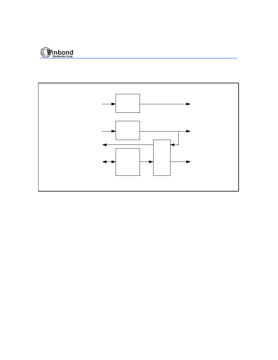
W9961CF
- 50 -
7.9 DRAM Controller
MA
Mux
MSIG
MD/BE
Mux
Arbitration
&
State
Machine
20-bit address
from FDMA, RISC,
PCI, VPRE, VPOST
32-bit data and 4-bit BEs
from FDMA, RISC,
PCI, VPRE, VPOST
DRAM request/cycle
from/to FDMA, RISC,
PCI, VPRE, VPOST
BA, MA[11:0]
MD[31:0]
RAS[1:0]#/CS[1:0]#,
CAS[3:0]#/DQM[3:0]#,
WE#, OE#/CKE,
SRAS#, SCAS#,
SMCLK
MDI[31:0]
Figure 7.16 DRAM Controller Block Diagram
A 32-bit SDRAM or EDO DRAM interface is supported for W9961CF. The DRAM Controller serves as
video memory arbiter and interface controller for video memory access.
7.9.1 Video Memory Arbitration
The video memory arbiter helps to maximize performance by orchestrating memory access requests
from internal engines. Three priority levels are defined for these requests:
� First priority: DRAM refresh request, SDRAM mode register write request
� Second priority: video capture request, graphics display request, VA1 request, VA2 request
� Third priority: FDMA request, RISC request, PCI request, pre-filter request, post-filter
request
First priority requests are for DRAM refresh and SDRAM mode control.
Second priority requests are for video input and video output, which should be real-time processed. A
FIFO status is provided by each request such that the DRAM Controller arbitrates according to these
FIFO status to prevent any video data loss.
Third priority requests are for video coding/decoding and bitstream transfers. Priorities of them can be
either RISC, pre-filter, FDMA, post-filter, then PCI access, or PCI, RISC, pre-filter, FDMA, then post-
filter access.
W9961CF
- 51 -
7.9.2 DRAM Interface
The DRAM controller provides many programmable controls for the DRAM operations which include:
� DRAM Type: supports SDRAM and EDO DRAM
� DRAM Address: programmable 9-bit (256K� EDO DRAM), 10-bit (1M� EDO DRAM or
256K
� SDRAM), and 12-bit (1M� SDRAM) address
� DRAM Timing: adjustable Trp, Trcd, Tras, and Tcas timings
� DRAM Refresh: 1 ~ 8 refresh cycles per scan line
� SDRAM Read Latency: 1 ~ 3 clocks
� SDRAM Burst Type: sequential or interleaved
� SDRAM Burst Length: 1, 2, 4, 8, or full page
Table 7.8 shows the interface signals for SDRAM and EDO DRAM.
Table 7.8 SDRAM and EDO DRAM Interface Signals
Pin Name
256K
� EDO
DRAM
1M
� EDO DRAM
256K
� SDRAM
1M
� SDRAM
MD[31:0]
MD[31:0]
MD[31:0]
MD[31:0]
MD[31:0]
MA[10:0]
MA[8:0]
MA[9:0]
MA[8:0]
MA[10:0]
BA
BA
BA
RAS[1:0]#/CS[1:0]#
RAS[1:0]#
RAS[1:0]#
CS[1:0]#
CS[1:0]#
CAS[3:0]#/DQM[3:0]
CAS[3:0]#
CAS[3:0]#
DQM[3:0]
DQM[3:0]
OE#/CKE
OE#
OE#
CKE
CKE
WE#
WE#
WE#
WE#
WE#
SRAS#
SRAS#
SRAS#
SCAS#
SCAS#
SCAS#
SMCLK
SMCLK
SMCLK

W9961CF
- 52 -
7.10 ISA-like Bus Interface and GPIOs
7.10.1 ISA-like Bus Interface
The ISA-like Bus provides a 13-bit address bus, an 8-bit data bus, one write strobe signal, one read
strobe signal, and one interrupt input as interface with an external co-processor. It can be accessed
directly by the host through PCI bus, or indirectly by the host or RISC via the ISA-like Bus Control
registers as described in Table 7.9. The external interrupt input can be either level-triggered
(ISAINT_2 = 1) or falling edge-triggered (ISAINT_2 = 0).
Table 7.9 ISA-like Bus Access Modes
Mode
Address Space
Description
PCI Direct Access
BA3 000000H ~ 00003FH
64-byte address space, byte-access only.
ISA-like Bus signals are automatically
generated when a PCI I/O read or write
command to this address space is issued.
PCI Indirect Access
BA1 0040H ~ 004CH
8K-byte address space. ISA-like Bus
signals are generated via the ISA-like Bus
Control registers.
RISC Indirect Access
RISC DM 000010H ~ 000013H
8K-byte address space. ISA-like Bus
signals are generated via the ISA-like Bus
Control registers.
7.10.2 GPIO
The W9961CF provides 5 general purpose I/O ports. Each GPIO can be configured as an input or
output port, depending on the corresponding bit of the GPIO Output Enable register (GPIOOE).
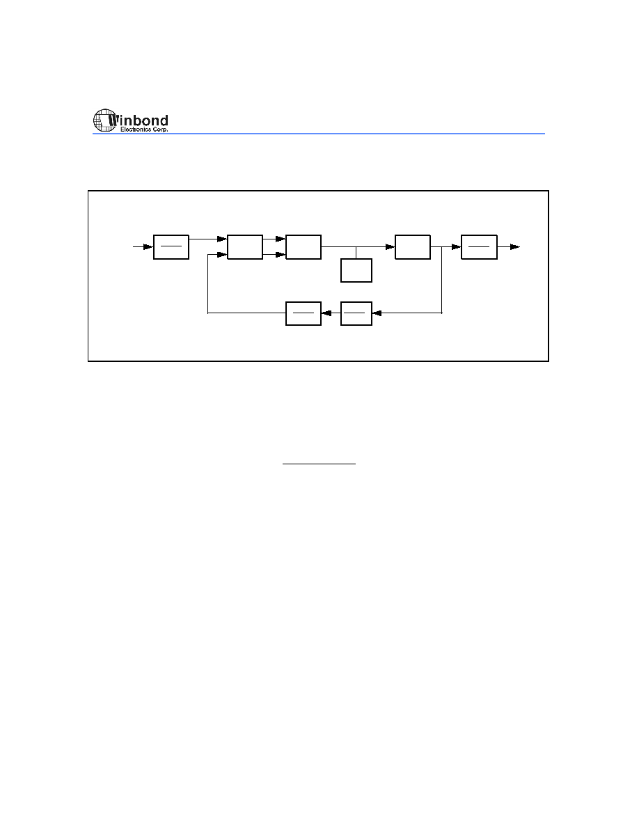
W9961CF
- 53 -
7.11 PLL (Phase Locked Loop)
1
(M+1)
PHASE
DETECT
CHARGE
PUMP
LOOP
FILTER
VCO
1
(N2+1)
1
2
K
f
REF
f
OUT
1
2
N1
Figure 7.17 PLL Block Diagram
The built-in PLL frequency synthesizer is used to generate the internal MCLK clock. A stable
reference frequency is required by dividing VOCLK by 2 (VOCLK/2 with typical 13.5 Mhz frequency)
as the reference clock input for the PLL. The output frequency resulting from a given set of
parameters is specified by the following formula:
f
N
M
f
OUT
N
K
REF
=
+ )
(
+ )
2
2
1
1
2
1
�
�
�
(
where M is a 6-bit value that can be programmed with any integer value from 1 to 63, N1 is a 2-bit
value that can be programmed with any integer value from 0 to 3, N2 is a 6-bit value that can be
programmed with any integer value from 1 to 127, and K is a 2-bit value that can be programmed
with any integer value from 0 to 3.

W9961CF
- 54 -
8 ELECTRICAL CHARACTERISTICS
8.1 Absolute Maximum Ratings
Table 8.1 Absolute Maximum Ratings
Ambient temperature
0
� C to 70� C
Storage temperature
-40
� C to 125� C
DC supply voltage
-0.5V to 7V
I/O pin voltage with respect to VSS
-0.5V to VDD + 0.5V
8.2 DC Characteristics
8.2.1 DAC DC Characteristics
Table 8.2 DAC DC Characteristics
Parameter
Min.
Typ.
Max.
Unit
Power Supply AVDD, TVAVDD
3.0
3.3
3.6
V
DAC Coding
Binary
TVDAC Resolution
9
9
9
Bits
Integral Linearity Error
�1
LSB
Differential Linearity Error
�1
LSB
Gray Scale Error
�5
%Gray
LSB Size
69.1
�A
DAC-to-DAC Matching
2
5
%
Output Compliance
-1.0
1.5
V
Gray Scale Current Range
35
mA
Output Impedance
10K
Output Capacitance (f = 1 MHz; IOUT = 0 mA)
30
pF
Monotonicity
Guaranteed
Internal VREF
1.06
V
Power Supply Reject Ratio (f = 1 KHz)
0.5
%%AVDD
Note 1. Measured with VREF = 1.06 V, RSET = 100
.
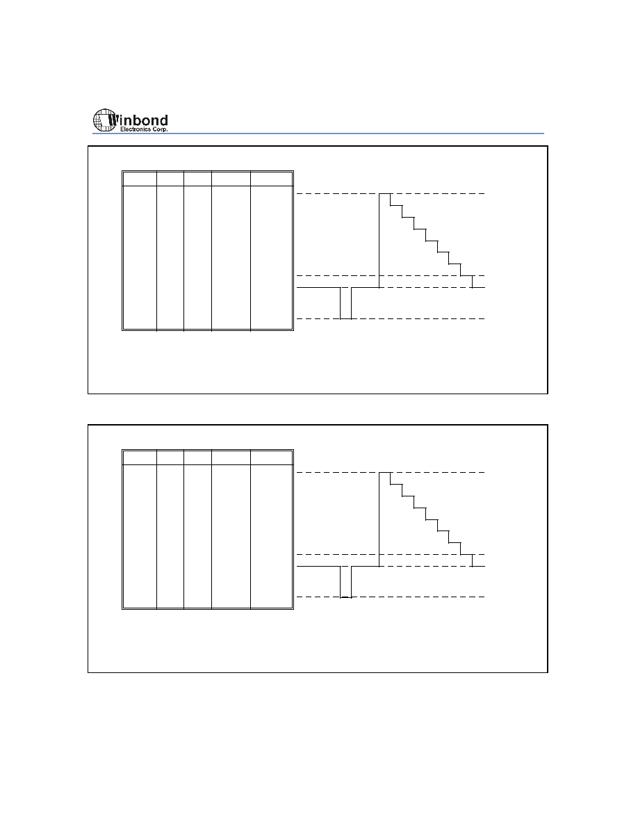
W9961CF
- 55 -
Level
White
Yellow
Cyan
Green
Magenta
Red
Blue
Black
Blank
Sync
mA
V
IRE
DAC Data
26.68
1.000
100.0000
400
89.4550
370
72.3425
321
61.7972
291
45.7025
245
35.1575
215
18.0450
166
9.07
0.340
7.5000
136
7.60
0.285
0.0000
114
0.00
0.000
-40.0000
0
Sync Level
Blank Level
Black Level
White Level
Note: Nominal RSET, 75
doubly-terminated load, with setup on.
SMPTE 170M levels are assumed. 100% saturation color bars (100/7.5/100/7.5).
Figure 8.1 525-line (NTSC/PAL-M) Y (Luminance) Output Waveform
Level
White
Yellow
Cyan
Green
Magenta
Red
Blue
Black
Blank
Sync
mA
V
IRE
DAC Data
26.68
1.000
100.0000
400
368
316
284
236
204
8.00
0.300
0.0000
120
8.00
0.300
0.0000
120
0.00
0.000
-43.0000
0
Sync Level
Blank Level
Black Level
White Level
Note: Nominal RSET, 75
doubly-terminated load, with setup off.
CCIR 624 levels are assumed. 100% saturation color bars (100/0/100/0).
152
Figure 8.2 625-line (PAL-B, D, G, H, N) Y (Luminance) Output Waveform
W9961CF
- 56 -
Color
Cyan/Red
Green/Magenta
Yellow/Blue
Burst High
Blank
Burst Low
Yellow/Blue
Green/Magenta
Cyan/Red
mA
V
IRE
DAC Data
28.21
1.058
58.5000
423
54.6000
41.4000
20.0000
313
0.0000
256
-20.0000
199
-41.4000
13.27
0.498
-54.6000
5.93
0.222
-58.5000
89
Note: Nominal RSET, 75
doubly-terminated load, with setup on.
SMPTE 170M levels are assumed. 100% saturation color bars (100/7.5/100/7.5).
Yellow
White
Cyan
Green
Magenta
Red
Blue
Black
Blank
Level
17.07
0.640
20.88
0.783
Color Burst
(9 Cycles)
Figure 8.3 525-line (NTSC/PAL-M) C (Chrominance) Output Waveform
Color
Cyan/Red
Green/Magenta
Yellow/Blue
Burst High
Blank
Burst Low
Yellow/Blue
Green/Magenta
Cyan/Red
mA
V
IRE
DAC Data
28.88
1.083
63.2500
433
59.0500
44.7500
21.5000
316
0.0000
256
-21.5000
196
-44.7500
13.07
0.490
-59.0500
5.27
0.198
-63.2500
79
Note: Nominal RSET, 75
doubly-terminated load, with setup off.
CCIR 624 levels are assumed. 100% saturation color bars (100/0/100/0).
Yellow
White
Cyan
Green
Magenta
Red
Blue
Black
Blank
Level
17.07
0.640
21.08
0.791
Color Burst
(10 Cycles)
Figure 8.4 625-line (PAL-B, D, G, H, N) C (Chrominance) Output Waveform

W9961CF
- 57 -
Level
White
Black
Blank
Sync
mA
V
IRE
DAC Data
26.68
1.000
100.0000
400
9.07
0.340
7.5000
136
7.60
0.285
0.0000
114
0.00
0.000
-40.0000
0
Sync Level
Blank Level
Black Level
White Level
Note: Nominal RSET, 75
doubly-terminated load, with setup on.
SMPTE 170M levels are assumed. 100% saturation color bars (100/7.5/100/7.5).
Peak Chroma
(High)
32.55
1.221
130.8333
488
Burst Low
3.80
0.143
-20.0000
57
Burst High
11.41
0.423
20.0000
171
Color Burst
(9 Cycles)
Yellow
White
Cyan
Green
Magenta
Red
Blue
Black
Peak Chroma
(Low)
3.20
0.120
-23.3333
48
Figure 8.5 525-line (NTSC/PAL-M) Composite Video Output Waveform
Level
White
Black
Blank
Sync
mA
V
IRE
DAC Data
26.68
1.000
100.0000
400
8.00
0.300
0.0000
120
8.00
0.300
0.0000
120
0.00
0.000
-43.0000
0
Sync Level
Blank Level
Black Level
White Level
Note: Nominal RSET, 75
doubly-terminated load, with setup off.
CCIR 624 levels are assumed. 100% saturation color bars (100/0/100/0).
Peak Chroma
(High)
32.88
1.233
133.3333
493
Burst Low
4.00
0.150
-21.5000
60
Burst High
12.01
0.450
21.5000
180
Color Burst
(10 Cycles)
Yellow
White
Cyan
Green
Magenta
Red
Blue
Black
Peak Chroma
(Low)
1.80
0.068
-33.3333
27
Figure 8.6 625-line (PAL-B, D, G, H, N) Composite Video Output Waveform

W9961CF
- 58 -
8.2.2 Digital DC Characteristics
Table 8.3 Digital DC Characteristics
Symbol
Parameter
Conditions
Min.
Max.
Unit
VDD5V
5V Power Supply
5.25
5.75
V
VDD
3V Power Supply
3.0
3.6
V
V
IL
Input Low Voltage
-0.5
0.8
V
V
IH
Input High Voltage
2.0
V
V
OL
Output Low Voltage
VSS+0.4
V
V
OH
Output High Voltage
2.4
V
I
IL
Input Low Leakage Current
V
IN
= 0.4V
+70
�A
I
IH
Input High Leakage Current
V
IN
= 2.4V
-70
�A
I
UP
Pull-up Current
V
IN
= 0V
-133.2
-400.6
�A
C
IO
Pin Capacitance
10
pF
I
DD
Active Current
F
MCLK
= 70 MHz
500
mA
W9961CF
- 59 -
8.3 AC Characteristics
8.3.1 DAC AC Characteristics
Table 8.4 DAC AC Characteristics
Parameter
Min.
Typ.
Max.
Unit
Luminance Bandwidth
Fin/2
MHz
Chrominance Bandwidth
1.3
MHz
Hue Accuracy
1.5
3
�
Color Saturation Accuracy
1.5
3
%
DAC Output Delay
30
ns
DAC Output Rise/Fall Time
3
ns
DAC Output Settling Time
8
ns
Input Clock Frequency (Fin)
12.27
13.5
14.75
MHz
Table 8.5 TV Modes Resolution and Clock Rate
Mode
Active Pixels
Total Pixels
TV Clock
NTSC
720x485
858x525
13.5000 MHz
PAL-M
720x484
858x525
13.5000 MHz
PAL-B, D, G, H, N
720x576
864x625
13.5000 MHz
8.3.2 PLL AC Characteristics
Table 8.6 PLL AC Characteristics
Parameter
Min.
Typ.
Max.
Unit
Input Clock Frequency
13.5
MHz
Input Clock Duty Cycle
40
50
60
%
MCLK Clock Frequency
70
MHz
MCLK Clock Frequency Error
0.5
%
MCLK Clock Duty Cycle
40
50
60
%

W9961CF
- 60 -
8.3.3 RESET Timing AC Characteristics
RST#
T
RST
T
SU
T
H
MD[15:0]
Figure 8.7 RESET Timing
Table 8.7 RESET Timing
Symbol
Parameter
Conditions
Min.
Max.
Unit
T
RST
Reset Pulse Width
100
ns
T
SU
MD[15:0] Setup Time
20
ns
T
H
MD[15:0] Hold Time
10
ns
8.3.4 Clock AC Characteristics
T
HIGH
T
LOW
T
CYC
0.8 V
1.5 V
2.0 V
Figure 8.8 Clock Waveform
Table 8.8 Clock AC Characteristics
Symbol
Parameter
Conditions
Min.
Max.
Unit
1/T
CYC
PCICLK Frequency
VICLK Frequency
VOCLK Frequency
VOCLK/2 Frequency
30
5
26.999
13.499
60
40
30
27.001
15.001
80
MHz
MHz
MHz
MHz
MHz

W9961CF
- 61 -
SMCLK Frequency
T
HIGH
PCICLK High Time
VICLK High Time
VOCLK High Time
VOCLK/2 High Time
SMCLK High Time
PCICLK = 33 Mhz
VICLK = 13.5 Mhz
VOCLK = 27 Mhz
VOCLK/2 = 13.5 Mhz
SMCLK = 70 MHz
12
29.6
14.8
29.6
5.7
18
44.5
22.3
44.5
8.6
ns
ns
ns
ns
ns
T
LOW
PCICLK Low Time
VICLK Low Time
VOCLK Low Time
VOCLK/2 Low Time
SMCLK Low Time
PCICLK = 33 Mhz
VICLK = 13.5 Mhz
VOCLK = 27 Mhz
VOCLK/2 = 13.5 Mhz
SMCLK = 70 MHz
12
29.6
14.8
29.6
5.7
18
44.5
22.3
44.5
8.6
ns
ns
ns
ns
ns
8.3.5 Input Timing AC Characteristics
CLK
INPUT
T
SU
T
H
1.5 V
1.5 V
1.5 V
input valid
Figure 8.9 Input Timing
Table 8.9 PCICLK-Referenced Input Timing AC Characteristics
Symbol
Parameter
Conditions
Min.
Max.
Unit
T
SU
AD[31:0], C/BE[3:0]#, FRAME#,
IRDY#, IDSEL
7
ns
T
H
AD[31:0], C/BE[3:0]#, FRAME#,
IRDY#, IDSEL
7
ns
Table 8.10 SMCLK-Referenced Input Timing AC Characteristics
Symbol
Parameter
Conditions
Min.
Max.
Unit
T
SU
MD[15:0] , SD[7:0] Setup Time
0
ns
T
H
MD[15:0] , SD[7:0] Hold Time
7
ns

W9961CF
- 62 -
Table 8.11 VICLK-Referenced Input Timing AC Characteristics
Symbol
Parameter
Conditions
Min.
Max.
Unit
T
SU
Y[7:0], UV[7:0], HS, VS
5
ns
T
H
Y[7:0], UV[7:0], HS, VS
5
ns
8.3.6 Output Timing AC Characteristics
CLK
OUTPUT
DELAY
T
VAL
1.5 V
1.5 V
T
ON
T
OFF
Tri-State
OUTPUT
Figure 8.10 Output Timing
Table 8.12 PCICLK-Referenced Output Timing AC Characteristics
Symbol
Parameter
Conditions
Min.
Max.
Unit
T
VAL
AD[31:0], TRDY#
2
11
ns
T
on
AD[31:0]
2
11
ns
DEVSEL#, TRDY#, INTA#, PAR,
PERR#, SERR#
2
11
ns
T
off
AD[31:0]
28
ns
DEVSEL#, TRDY#, INTA#, PAR,
PERR#, SERR#
28
ns
Table 8.13 SMCLK-Referenced Output Timing AC Characteristics
Symbol
Parameter
Conditions
Min.
Max.
Unit
T
VAL
MD[15:0], MA[10:0], BA,
RAS[1:0]#/CS[1:0]#,
CAS[1:0]#/DQM[1:0], OE#/CKE,
WE#, SRAS#, SCAS#
2
7
ns
SA[12:0], SD[7:0], SRD#, SWR#
2
11
ns
T
ON
MD[15:0]
2
7
ns
W9961CF
- 63 -
T
OFF
MD[15:0]
2
7
ns
Table 8.14 PCLK-Referenced Output Timing AC Characteristics
Symbol
Parameter
Conditions
Min.
Max.
Unit
T
VAL
HSYNC, VSYNC, P[7:0]
10
ns

W9961CF
- 64 -
9 PACKAGE SPEC.
The W9961CF is packaged in a 208L QFP (28x28 mm footprint 2.6mm) as shown in Figure 9.1.
H
D
D
e
b
E
H
E
y
A
A
Seating Plane
L
L
1
See Detail F
Detail F
c
1
A
2
1
52
53
104
105
156
157
208
0.10
0
10
10
0
0.004
1.30
0.70
30.90
30.90
0.50
30.60
30.60
0.30
30.30
30.30
0.051
0.028
1.217
1.217
0.020
1.205
1.205
0.012
1.193
1.193
0.50
28.13
28.13
0.25
0.25
3.35
3.68
28.00
28.00
3.23
27.87
27.87
0.10
0.15
3.10
0.10
1.107
1.107
0.010
0.010
0.132
0.145
1.102
1.102
0.127
0.020
1.097
1.097
0.004
0.006
0.122
0.004
Symbol
Min
Nom
Max
Max
Nom
Min
Dimension in inch
Dimension in mm
A
b
c
D
e
H
D
H
E
L
y
A
A
L
1
1
2
E
0.008
0.006
0.15
0.20
0.016
0.043
0.024
0.059
0.40
0.60
1.10
1.50
control dimensions are in mm
Figure 9.1 208L QFP (28X28 mm footprint 2.6mm) Dimensions

W9961CF
- 65 -
10 ORDERING INFORMATION
Part Number
Package
W9961CF
208L QFP
Headquarters
No. 4, Creation Rd. III,
Science-Based Industrial Park,
Hsinchu, Taiwan
TEL: 886-3-5770066
FAX: 886-3-5792647
http://www.winbond.com.tw/
Voice & Fax-on-demand: 886-2-7197006
Taipei Office
11F, No. 115, Sec. 3, Min-Sheng East Rd.,
Taipei, Taiwan
TEL: 886-2-7190505
FAX: 886-2-7197502
Winbond Electronics (H.K.) Ltd.
Rm. 803, World Trade Square, Tower II,
123 Hoi Bun Rd., Kwun Tong,
Kowloon, Hong Kong
TEL: 852-27513100
FAX: 852-27552064
Winbond Electronics North America Corp.
Winbond Memory Lab.
Winbond Microelectronics Corp.
Winbond Systems Lab.
2730 Orchard Parkway, San Jose,
CA 95134, U.S.A.
TEL: 1-408-9436666
FAX: 1-408-9436668
Note: All data and specifications are subject to change without notice.