
W9968CF
JPEG USB DUAL MODE CAMERA CHIP
Publication Release Date: May 1999
- 1 -
Revision A2
W9968CF
JPEG USB Dual Mode Camera Chip

W9968CF
- 2 -
Revision History
Revision
Issue Date
Comments
A1
April, 1998
Formal release.
A2
May, 1999
Supports USB Spec. Rev. 1.1. Changed bcdUSB and bcdDevice
values from 0x0100 to 0x0110. Added CR39_4 for JPEG clock
enable.
Copyright by Winbond Electronics Corp., all rights reserved.
The information in this document has been carefully checked and is believed to be correct as of the
date of publication. Winbond Electronics Corp. reserves the right to make changes in the product or
specification, or both, presented in this publication at any time without notice.
Winbond assumes no responsibility or liability arising from the specification listed herein. Winbond
makes no representations that the use of its products in the manner described in this publication will not
infringe on existing or future patents, trademark, copyright, or rights of third parties. No license is
granted by implication or other under any patent or patent rights of Winbond Electronics Corp.
All other trademarks and registered trademarks are the property of their respective holders.

W9968CF
Publication Release Date: May 1999
- 3 -
Revision A2
TABLE OF CONTENTS
1 GENERAL DESCRIPTION
.............................................................................................................. 7
2 FEATURES
....................................................................................................................................... 8
3 PIN CONFIGURATION
.................................................................................................................. 10
4 PIN DESCRIPTION
........................................................................................................................ 11
4.1 P
IN
D
EFINITION
.................................................................................................................................. 11
4.2 P
IN
L
IST
............................................................................................................................................. 16
4.3 P
OWER
-
ON
R
ESET
I
NITIALIZATION
..................................................................................................... 17
5 SYSTEM DIAGRAM
....................................................................................................................... 18
6 BLOCK DIAGRAM
......................................................................................................................... 19
7 FUNCTIONAL DESCRIPTION
...................................................................................................... 20
7.1 V
IDEO
I
NPUT
I
NTERFACE
.................................................................................................................... 20
7.1.1 Camera Control Serial Bus
...................................................................................................... 20
7.1.2 Input Video Data Format
.......................................................................................................... 20
7.1.3 Cropping
.................................................................................................................................... 21
7.1.4 Scaling
....................................................................................................................................... 21
7.1.5 Filtering
...................................................................................................................................... 22
7.1.6 Captured Video Data Format
................................................................................................... 22
7.2 DRAM C
ONTROL AND
I
NTERFACE
..................................................................................................... 23
7.2.1 DRAM Access Arbitration
........................................................................................................ 23
7.2.2 DRAM Interface
........................................................................................................................ 23
7.3 JPEG C
OMPRESSION
........................................................................................................................ 25
7.3.1 Level Shift and Forward DCT
.................................................................................................. 25
7.3.2 Quantization
.............................................................................................................................. 25
7.3.3 Huffman Encoding
.................................................................................................................... 26
7.3.4 JPEG Encoding Order
.............................................................................................................. 26
7.4 USB I
NTERFACE AND
D
EVICE
C
ONTROL
............................................................................................ 27
7.4.1 Endpoints
..................................................................................................................................... 27
7.4.1.1 Default Endpoint (Endpoint 0)
............................................................................................................27
7.4.1.2 Video Data-In Endpoint (Endpoint 1)
.................................................................................................27
7.4.2 USB Device Requests
.............................................................................................................. 27
7.4.2.1 Standard Device Requests
................................................................................................................27
7.4.2.2 Video Camera Class-Specific Requests
...........................................................................................29
7.4.2.3 Vendor-Specific Requests
.................................................................................................................29
7.4.3 Descriptors
................................................................................................................................ 30
7.4.3.1 Device Descriptors
.............................................................................................................................30
7.4.3.2 Configuration Descriptors
..................................................................................................................31
7.4.3.3 String Descriptors
...............................................................................................................................33
7.5 V
IDEO
/S
TILL
I
MAGE
D
ATA
T
RANSFER
................................................................................................. 34

W9968CF
- 4 -
7.5.1 Output Video Data Format
....................................................................................................... 34
7.5.2 Video Frame Synchronization
................................................................................................. 34
7.5.3 Bandwidth Management
.......................................................................................................... 34
7.6 P
OWER
M
ANAGEMENT
....................................................................................................................... 35
7.6.1 W9968CF Reset
....................................................................................................................... 35
7.6.2 Before Configured
.................................................................................................................... 35
7.6.3 After Configured
....................................................................................................................... 35
7.6.4 Suspend
.................................................................................................................................... 35
7.6.5 Resume
..................................................................................................................................... 36
7.7 S
ERIAL
EEPROM I
NTERFACE
........................................................................................................... 37
7.7.1 EEPROM Data Structure
............................................................................................................ 37
7.7.2 EEPROM Operations
............................................................................................................... 37
7.8 M
ICROCONTROLLER
I
NTERFACE
........................................................................................................ 39
7.8.1 Base Address Setup
................................................................................................................... 39
7.8.2 W9968CF Register Access
........................................................................................................ 39
7.8.3 Microcontroller Interrupt
.............................................................................................................. 39
7.8.4 DRAM Access
............................................................................................................................. 39
7.8.5 IHV-Specific Information
............................................................................................................. 40
8 CONTROL AND STATUS REGISTERS
...................................................................................... 41
8.1 G
ENERAL
C
ONTROL
R
EGISTERS
........................................................................................................ 43
8.2 V
IDEO
I
NPUT
C
ONTROL
R
EGISTERS
................................................................................................... 52
8.3 JPEG E
NCODER
C
ONTROL
R
EGISTERS
............................................................................................ 63
9 ELECTRICAL CHARACTERISTICS
............................................................................................ 70
9.1 A
BSOLUTE
M
AXIMUM
R
ATINGS
.......................................................................................................... 70
9.2 DC C
HARACTERISTICS
...................................................................................................................... 70
9.2.1 USB Transceiver DC Characteristics
...................................................................................... 70
9.2.2 Digital DC Characteristics
........................................................................................................ 70
9.3 AC C
HARACTERISTICS
...................................................................................................................... 71
9.3.1 USB Transceiver AC Characteristics
...................................................................................... 71
9.3.2 RESET Timing AC Characteristics
.......................................................................................... 72
9.3.3 Clock AC Characteristics
......................................................................................................... 73
9.3.4 Input Video AC Characteristics
............................................................................................... 73
9.3.5 DRAM Interface AC Characteristics
........................................................................................ 74
9.3.6 EEPROM Interface AC Characteristics
.................................................................................. 75
9.3.7 Microcontroller Interface AC Characteristics
.......................................................................... 76
10 PACKAGE SPEC.
........................................................................................................................ 77
11 ORDERING INFORMATION
....................................................................................................... 78

W9968CF
Publication Release Date: May 1999
- 5 -
Revision A2
LIST OF FIGURES
F
IGURE
3.1 W9968CF P
IN
C
ONFIGURATION
.................................................................................................. 10
F
IGURE
5.1 W9968CF-B
ASED
USB D
IGITAL
V
IDEO
C
AMERA
S
YSTEM
D
IAGRAM
........................................... 18
F
IGURE
6.1 W9968CF B
LOCK
D
IAGRAM
....................................................................................................... 19
F
IGURE
7.1 I
NPUT
V
IDEO
D
ATA
F
ORMATS
..................................................................................................... 21
F
IGURE
7.2 JPEG E
NCODING
O
RDER
............................................................................................................. 26
F
IGURE
7.3 D
EVICE
C
ONFIGURATION
............................................................................................................ 27
F
IGURE
7.4 EEPROM T
IMING
D
IAGRAM
....................................................................................................... 38
F
IGURE
9.1 D
ATA
S
IGNAL
R
ISE AND
F
ALL
T
IME
............................................................................................ 71
F
IGURE
9.2 D
IFFERENTIAL
D
ATA
J
ITTER
........................................................................................................ 71
F
IGURE
9.3 D
IFFERENTIAL TO
EOP T
RANSITION
S
KEW AND
EOP W
IDTH
....................................................... 71
F
IGURE
9.4 R
ECEIVER
J
ITTER
T
OLERANCE
..................................................................................................... 72
F
IGURE
9.5 RESET T
IMING
.......................................................................................................................... 72
F
IGURE
9.6 C
LOCK
W
AVEFORM
.................................................................................................................... 73
F
IGURE
9.7 I
NPUT
V
IDEO
T
IMING
.................................................................................................................. 73
F
IGURE
9.8 DRAM I
NTERFACE
I
NPUT
T
IMING
............................................................................................... 74
F
IGURE
9.9 DRAM I
NTERFACE
O
UTPUT
T
IMING
............................................................................................ 74
F
IGURE
9.10 EEPROM I
NTERFACE
T
IMING
................................................................................................... 75
F
IGURE
9.11 M
ICROCONTROLLER
I
NTERFACE
T
IMING
.................................................................................... 76
F
IGURE
10.1 128L QFP (14
X
20
X
2.75
MM FOOTPRINT
3.2
MM
) D
IMENSIONS
....................................................... 77

W9968CF
- 6 -
LIST OF TABLES
T
ABLE
4.1 W9968CF P
IN
L
IST
.................................................................................................................... 16
T
ABLE
4.2 P
OWER
-
ON
R
ESET
C
ONFIGURATION
D
EFINITIONS
...................................................................... 17
T
ABLE
7.1 C
APTURED
V
IDEO
D
ATA
F
ORMAT
............................................................................................... 22
T
ABLE
7.2 SDRAM
AND
EDO DRAM I
NTERFACE
S
IGNALS
........................................................................ 23
T
ABLE
7.3 S
TANDARD
D
EVICE
R
EQUESTS
................................................................................................... 28
T
ABLE
7.4 W9968CF V
ENDOR
-S
PECIFIC
R
EQUESTS
.................................................................................. 29
T
ABLE
7.5 W9968CF D
EVICE
D
ESCRIPTOR
................................................................................................ 30
T
ABLE
7.6 W9968CF C
ONFIGURATION
D
ESCRIPTOR
.................................................................................. 31
T
ABLE
7.7 W9968CF V
IDEO
I
NTERFACE
D
ESCRIPTOR
............................................................................... 31
T
ABLE
7.8 W9968CF D
ATA
-I
N
E
NDPOINT
D
ESCRIPTOR
............................................................................. 32
T
ABLE
7.9 W9968CF V
IDEO
I
NTERFACE
A
LTERNATE
S
ETTING
1-16 I
NTERFACE
D
ESCRIPTOR
................... 32
T
ABLE
7.10 W9968CF A
LTERNATE
S
ETTING
1-16 D
ATA
-I
N
E
NDPOINT
D
ESCRIPTOR
................................. 32
T
ABLE
7.11 T
HE
M
AXIMUM
D
ATA
P
AYLOAD
S
IZE IN
B
YTES FOR
A
LTERNATE
S
ETTINGS
............................... 33
T
ABLE
7.12 W9968CF D
EFAULT
S
TREAM
D
ESCRIPTORS
........................................................................... 33
T
ABLE
7.13 O
UTPUT
V
IDEO
D
ATA
F
ORMAT
................................................................................................. 34
T
ABLE
7.14 EEPROM D
ATA
S
TRUCTURE
..................................................................................................... 37
T
ABLE
8.1 W9968CF C
ONTROL
R
EGISTER
M
AP
........................................................................................... 41
T
ABLE
9.1 A
BSOLUTE
M
AXIMUM
R
ATINGS
...................................................................................................... 70
T
ABLE
9.2 USB T
RANSCEIVER
DC C
HARACTERISTICS
.................................................................................. 70
T
ABLE
9.3 D
IGITAL
DC C
HARACTERISTICS
..................................................................................................... 70
T
ABLE
9.4 USB T
RANSCEIVER
AC C
HARACTERISTICS
................................................................................... 72
T
ABLE
9.5 RESET T
IMING
............................................................................................................................. 73
T
ABLE
9.6 C
LOCK
AC C
HARACTERISTICS
...................................................................................................... 73
T
ABLE
9.7 I
NPUT
V
IDEO
AC C
HARACTERISTICS
............................................................................................. 74
T
ABLE
9.8 DRAM I
NTERFACE
AC C
HARACTERISTICS
.................................................................................... 74
T
ABLE
9.9
EEPROM I
NTERFACE
AC C
HARACTERISTICS
............................................................................... 75
T
ABLE
9.10 M
ICROCONTROLLER
I
NTERFACE
AC C
HARACTERISTICS
.............................................................. 76

W9968CF
Publication Release Date: May 1999
- 7 -
Revision A2
1 GENERAL DESCRIPTION
The W9968CF is a digital video processing chip offered by Winbond to facilitate adapterless connection
between digital video camera and personal computer for video and still image capturing and editing,
video e-mail, and video conferencing applications. Low-cost, high-performance, and high-quality digital
video camera can be realized by using Winbond
s W9968CF, which includes Universal Serial Bus
(USB) technology and the international standard JPEG compression.
The digital video camera is becoming the next great input device for the PC. USB is now a common PC
standard for connecting peripheral products, which features low cost, hot-attachable plug and play,
adequate 12 Mb/s full speed bandwidth, and simultaneous attachment of multiple devices. The
W9968CF has built-in full speed USB controller which benefits from using the isochronous data transfer
mode of the USB bus, and which is compliant with the full power management requirements of the USB
specification, including startup, operating, and suspend modes. To prevent saturation of the USB bus,
the W9968CF uses no more than 8 Mb/s of available bandwidth to ensure the continued operation of
other low bandwidth devices such as USB mice and keyboards.
Although USB provides a low-cost solution for low to medium speed peripherals, its 12 Mb/s bandwidth
is not enough for high-quality and high-performance digital video camera. High-quality and low-cost
compression is necessary to boost frame rate for a high-performance digital video camera. The
W9968CF has built-in the baseline JPEG compression, which corresponds to the ISO/IEC international
standard 10918-1, with YCbCr4:2:2 or YCbCr4:2:0 components in non-interleaved scan. The baseline
JPEG implementation in the W9968CF includes Discrete Cosine Transform (DCT), quantization, zig-
zag scan, and Huffman encoder. With JPEG compression, the W9968CF can easily achieve good
quality 30 frames per second (fps) in CIF resolution (352
�
288) and 10~15 fps in VGA resolution
(640
�
480) by consuming no more than 8 Mb/s USB bandwidth.
The W9968CF can accept NTSC, PAL, or VGA video in 8- or 16-bit YCbCr4:2:2 format, square or
rectangular pixels, and converts to sub-QCIF (128
�
96), QCIF (176
�
144), CIF (128
�
96), SIF (352
�
240),
320
�
240, or VGA (640
�
480) format. Built-in cropping window control and arbitrary scaling in both the
horizontal and vertical directions can serve as the digital pan and zoom over a user-specified region for
camera control.
In addition to USB interface, the W9968CF also supports an 8-bit microcontroller interface for portable
PC camera applications. Up to 24 still images in 640
�
480 VGA format can be captured, JPEG
compressed, and stored into an external 2 Mbytes Flash memory when in the portable mode.
An on-chip DRAM controller is used to interface to SDRAM or EDO DRAM through a 16-bit data bus.
An external serial E
2
PROM is also supported if IHV-specific Vendor ID and Product ID are needed. The
IHV-specific information can be also provided by an external microcontroller if present to save the cost
of an E
2
PROM. The W9968CF is a 3.3 V device with TTL-compatible 3.3 V or 5.0 V I/O, and is
packaged in a 128L QFP.

W9968CF
- 8 -
2 FEATURES
q
USB Interface
�
Fully compliant with USB Specification Revision 1.1
�
Supports for full speed devices with maximum 12 Mb/s USB bandwidth
�
Uses no more than 8 Mb/s USB bandwidth to prevent saturation of the USB bus
�
Provides multiple alternate settings for various isochronous bandwidth consumptions
�
Does not use isochronous bandwidth for default alternate setting 0
�
Complies with USB power management requirements
�
USB Control and Isochronous transfers
�
On-chip USB full speed transceivers
�
Bus-powered high power devices
q
Video Compression
�
Fully compliant with ISO/IEC 10918-1 international JPEG standard
�
On-chip DCT, quantization, zig-zag scan, and Huffman encoder
�
Contains two AC and two DC Huffman code tables, and two programmable quantization tables
�
Supports baseline sequential mode in YCbCr4:2:2 or YCbCr4:2:0 non-interleaved scan
�
Encodes in sub-QCIF (128x96), QCIF (176x144), CIF (352x288), SIF (352x240), 320x240, or VGA
(640x480) picture format
�
Encodes sub-QCIF/QCIF/CIF/SIF/320x240 format at 30 frames per second (fps), VGA format at
10~15 fps
q
Video Pre-processing
�
Direct connect to digital camera through an 8- or 16-bit data bus
�
Glueless interface to NTSC/PAL TV decoder
�
Input video format compliant with YCbCr 4:2:2 CCIR 601 standard
�
Built-in cropping, arbitrary scaling, and filtering functions for digital pan and zoom camera control

W9968CF
Publication Release Date: May 1999
- 9 -
Revision A2
q
Video Output
�
Video output can be either compressed bit stream or original video
�
Compressed bit stream is fully compliant with ISO baseline JPEG standard in YCbCr4:2:2 or
YCbCr4:2:0 non-interleaved scan
�
Original video output can be in YCbCr4:2:2 or YCbCr4:2:0 packed format
q
DRAM Interface
�
Supports SDRAM or 1-cycle EDO DRAM
�
Supports SDRAM Self Refresh
�
Supports 16-bit DRAM interface in 0.5, 1, 2 or 4 Mbytes configuration
q
Serial EEPROM Interface
�
Supports optional 1K (128
�
8) serial EEPROM for IHV-specific Vendor ID and Product ID
q
Supports Hardware and Software Snap Shot
q
Supports 8-bit Microcontroller Interface for Portable PC Camera Applications
q
Built-in PLL (Phase-Locked Loops) Clock Synthesizer
q
Operating Frequency is 48 MHz with Video Input Frequency of 13.5 MHz (typical)
q
3.3 V Device with TTL-compatible 3.3 V or 5.0 V I/O
q
128L QFP Package
W9968CF
- 10 -
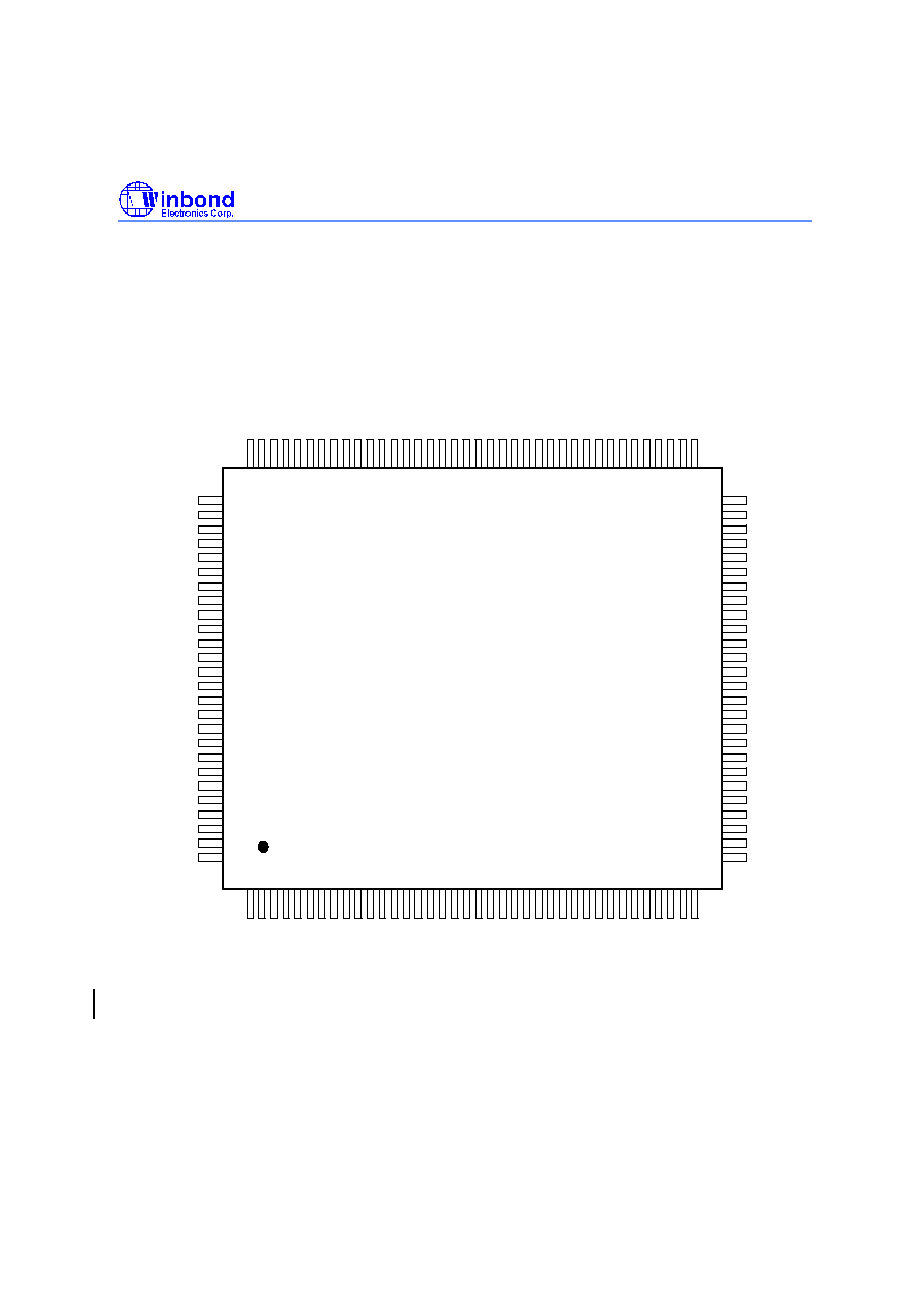
3 PIN CONFIGURATION
The W9968CF is packaged in a 128L QFP. The pin configuration is shown in Figure 3.1.
1
2
3
4
5
6
7
8
9
10
11
12
13
14
15
16
17
18
19
20
21
22
23
24
45
46
47
48
49
50
39
40
(Top View)
W9968CF
DP
DM
USBVDD
VSSI
VSSI
VSSP
25
26
27
28
29
30
41
42
43
44
VDDI
VDDI
VSSP
VDDP
MD6
MD8
MD7
VDDP
CAS1#/DQM1
CAS0#/DQM0
OE#/CKE
WE#
SCAS#
SRAS#
RAS0#/CS0#
SMCLK
VSSP
BA
MA10
MA9
MA8
MA7
MA6
MA1
MA5
MA2
MA4
MA3
MD13
MD14
MD15
UV0
UV1
UV2
UV3
UV4
UV5
UV6
UV7
VDDP
USBVSS
VSSP
XIN
XOUT
VDDP
MA0
VSSP
RAS1#/CS1#
VDDP
VSSP
MD2
SDE#/SDS
MD1
MD0
SCLK
VSSP
RSTIN#
RSTOUT
SUSPND
PWRDWN
VDDP
SDA/EEPROM
PWRDWN#
SCL
MD9
SDATA
INTXTR
31
32
33
34
65
51
52
53
103
35
36
37
38
54
55
56
57
58
59
60
61
62
63
64
66
67
68
69
70
71
72
73
74
75
76
77
78
79
80
81
82
83
84
85
86
87
88
89
90
91
92
93
94
95
96
97
98
99
100
101
102
104
105
106
107
108
109
110
111
112
113
114
115
116
117
118
119
120
121
122
123
124
125
126
127
128
VSSI
VSSP
MD4
MD10
MD5
MD11
MD3
VS
HS
Y0
Y1
Y2
Y3
Y4
Y5
Y6
Y7
VDDP
RD#
WR#
ALE
AD0
AD1
AD2
AD3
AD4
AD5
AD6
AD7
INT#
CLK24M
TEST#
RCV
VPO
VSSP
VICLK
MD12
VDD5V
VDDI
A8/GPIO0
VMO
TOE#
VP
VM
AVDD
AVSS
A9/GPIO1
A10/GPIO2
A11/GPIO3
A12/GPIO4
A13/GPIO5
A14/GPIO6
A15/GPIO7
EXTMCU
CS#/SNAP#
Figure 3.1 W9968CF Pin Configuration

W9968CF
Publication Release Date: May 1999
- 11 - Revision A2
4 PIN DESCRIPTION
The following signal types are used in these descriptions.
I
Input pin
IU
Input pin with internal pull-up resistor
B
Bi-directional input/output pin
O
Output pin
AIO
Analog input/output pin
P
Power supply pin
G
Ground pin
#
Active low
4.1 Pin Definition
USB and External Transceiver Interface (8 pins)
Pin Name
Pin Number
Type
Description
DM
50
AIO
Data Minus line of differential USB upstream port.
DP
51
AIO
Data Plus line of differential USB upstream port.
Note: provide an external 1.5 K
pull-up resistor at DP so the
device indicates to the host that it is a full-speed device.
VM
53
IU
Single-ended Receiver Input of the data minus line.
VP
54
IU
Single-ended Receiver Input of the data plus line.
RCV
55
IU
Differential Receiver Input.
TOE#
57
O
Output Enable for external transceiver.
VMO
58
O
Data Minus Output to the differential driver.
VPO
59
O
Data Plus Output to the differential driver.
DRAM Interface (37 pins)
Pin Name
Pin Number
Type
Description
MD[15:0]
92-95, 97-106,
109-110
B
Data Bus.
MA[10:0]
65-68, 70, 72-
77
O
Address Bus.
Note: for SDRAM, MA[10:0] are sampled during the ACTIVE

W9968CF
- 12 -
command (row address MA[10:0]) and READ/WRITE command
(column address MA[7:0], with MA10 defining AUTO
PRECHARGE) to select one location out of the 521K available in
the respective bank. MA10 is sampled during a PRECHARGE
command to determine if all banks are to be precharged (MA10
HIGH).
BA
78
O
EDO DRAM: Not used.
SDRAM: Bank Address Input. BA defines to which internal bank
the ACTIVE, READ, WRITE or PRECHARGE command is being
applied. BA is also used to program the 12th bit of the Mode
Register.
RAS[1:0]#
CS[1:0]#
80, 81
O
EDO DRAM: Row Address Strobes.
SDRAM: Chip Select. CS# enables the command decoder for
the SDRAM.
CAS[1:0]#
DQM[1:0]
89, 90
O
EDO DRAM: Column Address Strobes.
SDRAM: Input/Output Mask. DQM[1:0] are input mask signals
for write accesses and output enable signals for read accesses.
DQM0 corresponds to MD[7:0]; DQM1 corresponds to MD[15:8].
OE#
CKE
84
O
EDO DRAM: Output Enable.
SDRAM: Clock Enable. CKE activates the SMCLK signal. The
SDRAM enters precharge power-down to deactivate the input
and output buffers, excluding CKE, for maximum power saving
when CKE is LOW coincident with a NOP.
WE#
88
O
EDO DRAM: Write Enable.
SDRAM: Command Input. SRAS#, SCAS#, and WE# (along with
CS#) define the command being entered.
SRAS#
82
O
EDO DRAM: Not used.
SDRAM: Command Input. SRAS#, SCAS#, and WE# (along with
CS#) define the command being entered.
SCAS#
85
O
EDO DRAM: Not used.
SDRAM: Command Input. SRAS#, SCAS#, and WE# (along with
CS#) define the command being entered.
SMCLK
86
O
EDO DRAM: Not used.
SDRAM: Clock.
Input Video Interface (22 pins)
Pin Name
Pin Number
Type
Description
Y[7:0]
117-120, 122-
125
I
Digital Y (Luminance) Inputs in 16-bit Mode, or Digital YUV
Inputs in 8-bit Mode.
W9968CF
Publication Release Date: May 1999
- 13 - Revision A2
UV[7:0]
2-9
I
Digital UV (Chrominance) Inputs in 16-bit Mode, or Not Used in
8-bit Mode.
HS
116
I
Horizontal Sync Input. Programmable polarity.
VS
115
I
Vertical Sync Input. Programmable polarity.
VICLK
127
I
Input Video Clock.
SDE#/SDS
112
O
Serial Data Enable/Serial Data Strobe.
SCLK
113
B
Serial Interface Clock.
SDATA
114
B
Serial Interface Data.
Micro Controller Interface (21 pins)
Pin Name
Pin Number
Type
Description
AD[7:0]
21-24, 26-29
B
Multiplexed Address/Data Bus.
A[15:8]
GPIO[7:0]
31-38
I
B
EXTMCU = 1: High-order Address Bus.
EXTMCU = 0: General Purpose I/Os.
ALE
18
I
Address Latch Enable. ALE is used to enable the address latch
that separates the address from the data on AD bus.
RD#
15
IU
Data Read Strobe.
WR#
16
IU
Data Write Strobe.
CS#
SANP#
17
IU
EXTMCU = 1: Chip Select.
EXTMCU = 0: Snap Shot Input.
INT#
14
O
Interrupt Output, level-triggered.
Serial E
2
PROM Interface (2 pins)
Pin Name
Pin Number
Type
Description
SCL
62
O
Serial Clock.
SDA/EEPRO
M
63
B
Serial Data/Serial E
2
PROM Detection. During a reset operation,
the W9968CF samples this signal to see if an external E
2
PROM
exists. A 10K ohm pull-up resistor should be used if an external
E
2
PROM is used; otherwise it should be tied to VSS.
Miscellaneous (11 pins)
Pin Name
Pin Number
Type
Description
W9968CF
- 14 -
XIN
11
I
Reference frequency input from a crystal or a clock source. It
should be 48 Mhz if PLL is off (PLLSEL = 0) or 12 Mhz if PLL is
on (PLLSEL = 1) for full-speed device.
XOUT
12
O
Oscillator output to a crystal. This pin is left unconnected if an
external clock source is employed.
CLK24M
20
O
24 Mhz Clock Output.
EXTMCU
39
I
External Micro Controller (MCU). 0: no; 1: yes.
TEST#
40
IU
Test Input.
INTXTR
44
I
Internal USB Transceiver Select. 0: off; 1: on.
RSTIN#
45
IU
System Reset Input.
PWRDWN#
46
O
Low-active Power Down Control. This pin is active upon reset,
suspended, or when the Camera Power-on Control register
(CR00_4) is 0. Once active, it remains active until the CR00_4 is
set to 1.
PWRDWN
47
O
High-active Power Down Control. This pin is active upon reset,
suspended, or when the Camera Power-on Control register
(CR00_4) is 0. Once active, it remains active until the CR00_4 is
set to 1.
SUSPND
48
O
USB Suspend Mode. This pin is active when the W9968CF is in
the suspend mode. It is cleared to 0 when the W9968CF is
resumed, or reset by RSTIN# pin or a USB reset command.
RSTOUT
56
O
Reset Output. This pin is active when RSTIN# pin is active, or a
USB reset command is received.
Power and Ground (27 pins)
Pin Name
Pin Number
Type
Description
VDD5V
128
P
5V Buffer Power Supply. Provide 5V power to the I/O buffers for
5V input tolerance. +4.4 V ~ +5.25 V.
VDDP
1, 13, 30, 61,
71, 91, 107
P
Buffer Power Supply. Provide isolated power to the I/O buffers
for improved noise immunity. +3.3 V
�
0.3 V.
VSSP
10, 25, 64, 69,
79, 87, 96,
111, 126
G
Buffer Ground.
USBVDD
52
P
USB Transceiver Power Supply. +3.3 V
�
0.3 V.
USBVSS
49
G
USB Transceiver Ground.
AVDD
42
P
PLL Power Supply. +3.3 V
�
0.3 V.
AVSS
43
G
PLL Ground.
VDDI
19, 60, 108
P
Core Logic Power Supply. +3.3 V
�
0.3 V.

W9968CF
Publication Release Date: May 1999
- 15 - Revision A2
VSSI
41, 83, 121
G
Core Logic Ground.

W9968CF
- 16 -
4.2 Pin List
Table 4.1 W9968CF Pin List
Pin
Name
Pin
Name
Pin
Name
Pin
Name
1
VDDP
33
A10/GPIO2
65
MA3
97
MD5
2
UV0
34
A11/GPIO3
66
MA4
98
MD10
3
UV1
35
A12/GPIO4
67
MA2
99
MD4
4
UV2
36
A13/GPIO5
68
MA5
100
MD11
5
UV3
37
A14/GPIO6
69
VSSP
101
MD3
6
UV4
38
A15/GPIO7
70
MA1
102
MD12
7
UV5
39
EXTMCU
71
VDDP
103
MD2
8
UV6
40
TEST#
72
MA6
104
MD13
9
UV7
41
VSSI
73
MA0
105
MD1
10
VSSP
42
AVDD
74
MA7
106
MD14
11
XIN
43
AVSS
75
MA10
107
VDDP
12
XOUT
44
INTXTR
76
MA8
108
VDDI
13
VDDP
45
RSTIN#
77
MA9
109
MD0
14
INT#
46
PWRDWN#
78
BA
110
MD15
15
RD#
47
PWRDWN
79
VSSP
111
VSSP
16
WR#
48
SUSPND
80
RAS0#/CS0#
112
SDE#/SDS
17
CS#/SNAP#
49
USBVSS
81
RAS1#/CS1#
113
SCLK
18
ALE
50
DM
82
SRAS#
114
SDATA
19
VDDI
51
DP
83
VSSI
115
VS
20
CLK24M
52
USBVDD
84
OE#/CKE
116
HS
21
AD0
53
VM
85
SCAS#
117
Y0
22
AD1
54
VP
86
SMCLK
118
Y1
23
AD2
55
RCV
87
VSSP
119
Y2
24
AD3
56
RSTOUT
88
WE#
120
Y3
25
VSSP
57
TOE#
89
CAS0#/DQM0
121
VSSI
26
AD4
58
VMO
90
CAS1#/DQM1
122
Y4
27
AD5
59
VPO
91
VDDP
123
Y5
28
AD6
60
VDDI
92
MD7
124
Y6
29
AD7
61
VDDP
93
MD8
125
Y7
30
VDDP
62
SCL
94
MD6
126
VSSP
31
A8/GPIO0
63
SDA/EEPROM
95
MD9
127
VICLK
32
A9/GPIO1
64
VSSP
96
VSSP
128
VDD5V
Note 1. All output and bi-directional pins, except XOUT pin, are tri-stated during reset.

W9968CF
Publication Release Date: May 1999
- 17 - Revision A2
4.3 Power-on Reset Initialization
During power-on reset, states of the memory data lines MD[7:0] are latched into the W9968CF
s
internal configuration registers as device configuration information. Since each pin of MD[7:0] is
internally pulled up on its I/O buffer, no external pull-up resistor is required. For pull-down, a 4.7K ohm
resistor is recommended. Table 4.2 describes the power-on reset configuration definitions.
Table 4.2 Power-on Reset Configuration Definitions
MD Bit
Value
Definition
Conf Reg
MD7
0
1
Normal operation
Force suspend mode if suspend mode is enabled
CR00_15
MD6
0
1
Suspend mode is disabled
Suspend mode is enabled
CR00_14
MD5
0
1
Isochronous handshake phase is enabled
Isochronous handshake phase is disabled
CR00_13
MD4
0
1
Internal RCV comes from SIE
Internal RCV comes from USB Transceiver
CR00_12
MD3
0
1
PLL Disable
PLL Enable
CR00_11
MD2
0
1
Low Power, Bus-powered Devices
High Power, Bus-powered Devices
CR00_10
MD1
0
1
EDO DRAM
SDRAM
CR00_9
MD0
0
1
256Kx DRAM
1Mx DRAM
CR00_8

W9968CF
- 18 -
5 SYSTEM DIAGRAM
W9968CF
JPEG or original
Video
USB
Video Memory
1Mx16 SDRAM
YCbCr 4:2:2
Sensor
DSP
CCD/CMOS
Sensor
Serial E
2
PROM
128x8
8-bit
uC
optional
optional
Figure 5.1 W9968CF-Based USB Digital Video Camera System Diagram

W9968CF
Publication Release Date: May 1999
- 19 - Revision A2
6 BLOCK DIAGRAM
Video In
YCbCr 4:2:2
VPRE
DRAM Controller
Video Memory
D+
Serial E
2
PROM
W9968CF
DCT
Quantization
Zig-zag
VLE
Device Controller
USB SIE
USB
XCVRs
D-
8-bit uC
PLL
XIN
XOUT
Figure 6.1 W9968CF Block Diagram

W9968CF
- 20 -
7 FUNCTIONAL DESCRIPTION
7.1 Video Input Interface
Video input data is cropped, down-scaled, and filtered in the video pre-processing (VPRE) block, then
is stored into the DRAM as captured video for the following JPEG compression and transfer.
7.1.1 Camera Control Serial Bus
A dedicated programmable serial bus is supported for camera control. The serial bus includes SCLK,
SDATA, and SDE#/SDS signals. During serial bus read, these signals are controlled by the host via bits
4-0 of the Serial Bus Control register (CR01_4-0).
There are two serial bus write modes which are controlled by bit 5 of the Serial Bus Control register
(CR01_5).: normal serial bus write mode (CR01_5 = 0) and fast serial bus write mode (CR01_5 = 1).
Normal serial bus write mode (CR01_5 = 0): SDATA and SCLK signals are output from CR01_1-0
directly.
Fast serial bus write mode (CR01_5 = 1): SDATA and SCLK signals are output from CR06-CR09 in
about 400 Khz bit frequency.
7.1.2 Input Video Data Format
The W9968CF accepts video data in YUV 4:2:2 format through a 16-bit (Y[7:0] and UV[7:0]) or 8-bit
(Y[7:0]) data bus. Many YUV ordering formats are supported which are selected by bits 9-8 of the Video
Capture Control register (CR26) as shown in Figure 7.1. Video data can be latched by the W9968CF by
using either rising-edge or falling-edge of the VICLK clock signal. In the 8-bit modes the VICLK
frequency is twice the pixel rate, only Y[7:0] pins are used for video data input and UV[7:0] pins are not
used.

W9968CF
Publication Release Date: May 1999
- 21 - Revision A2
VICLK
16-bit UV Mode (CR26_10-8=00x)
Y0
Y1
Y2
Y3
Y4
Y5
Y6
U0
V0
U2
V2
U4
V4
U6
Y[7:0]
UV[7:0]
16-bit VU Mode (CR26_10-8=01x)
Y0
Y1
Y2
Y3
Y4
Y5
Y6
V0
U0
V2
U2
V4
U4
V6
Y[7:0]
UV[7:0]
8-bit YUYV Mode (CR26_10-8=100)
Y0
U0
Y1
V0
Y2
U2
Y3
Y[7:0]
8-bit UYVY Mode (CR26_10-8=101)
U0
Y0
V0
Y1
U2
Y2
V2
Y[7:0]
8-bit YVYU Mode (CR26_10-8=110)
Y0
V0
Y1
U0
Y2
V2
Y3
Y[7:0]
8-bit VYUY Mode (CR26_10-8=111)
V0
Y0
U0
Y1
V2
Y2
U2
Y[7:0]
Figure 7.1 Input Video Data Formats
7.1.3 Cropping
A cropping rectangle (or window) is supported for cropping or clipping the incoming video data. Only
interested video data located inside the cropping rectangle is processed and sent to the host system.
The cropping rectangle can be moved within the input rectangle by programming the Cropping Window
Start X and Cropping Window Start Y registers. Cropping is performed based on the VS signal for
vertical cropping and HS signal for horizontal cropping. Both VS and HS are programmable polarity for
maximum flexibility.
7.1.4 Scaling
The cropped video can be down-scaled horizontally and/or vertically. The horizontal down-scaling and
vertical down-scaling are performed independently by using two DDAs (Digital Differential Accumulator)
with
Horizontal Down - scaling Factor
Captured Video Width
Cropping Window End X
Cropping Window Start X
and
Vertical Down - scaling Factor
Captured Video Height
Cropping Window End Y
Cropping Window Start Y
.
=
-
=
-
The W9968CF does not perform up-scaling during video pre-processing. To produce CIF format from
240-line video for the JPEG compression, a special vertical up-scaling can be performed by the JPEG

W9968CF
- 22 -
encoder. For the original video transfer, the CIF format from 240-line video can be produced by the
software driver.
7.1.5 Filtering
A 3-tap or 5-tap FIR filter is used to reduce noise and aliasing artifacts produced by the CCD or CMOS
sensor, and the scaling process.
7.1.6 Captured Video Data Format
After cropped, down-scaled, and filtered in the video pre-processing (VPRE) block, the input video is
stored into the DRAM as captured video. Four different formats are supported for the captured video:
YUV4:2:2 packed, YUV4:2:0 packed, YUV4:2:2 planar, and YUV4:2:0 planar modes, which are
selected by bits 1-0 of the Video Capture Control register (CR26) as described in Table 7.1. YUV4:2:2
and YUV4:2:0 packed modes are used for original video transfer, while YUV4:2:2 and YUV4:2:0 planar
modes are used for JPEG compression video transfer.
Table 7.1 Captured Video Data Format
CR26_1-0
Captured Video Data Format
00
YUV4:2:2 packed mode for original video transfer
01
YUV4:2:0 packed mode for original video transfer
10
YUV4:2:2 planar mode for JPEG compression video transfer
11
YUV4:2:0 planar mode for JPEG compression video transfer

W9968CF
Publication Release Date: May 1999
- 23 - Revision A2
7.2 DRAM Control and Interface
The W9968CF supports 256K
�
16 and 1M
�
16 SDRAM or EDO DRAM in a 0.5 ~ 4 Mbytes configuration
with 16-bit data bus. A single 1M
�
16, -15 or above, SDRAM is recommended for better
cost/performance.
7.2.1 DRAM Access Arbitration
The DRAM arbiter helps to maximize performance by orchestrating memory access requests from
internal engines. Two priority levels are defined for these requests:
�
First priority: DRAM refresh request and SDRAM mode register write request
�
Second priority: Capture FIFO write request, DCT read request, VLE read request, VLE FIFO
write request, USB FIFO read request, and USB control read/write request
Programmable FIFO status are provided by the Capture FIFO, VLE FIFO, and USB FIFO such that the
DRAM Controller arbitrates according to these FIFO status to prevent any video data loss and to
achieve the best performance.
7.2.2 DRAM Interface
The DRAM controller provides many programmable controls for the DRAM operations which include:
�
DRAM Type: supports SDRAM and EDO DRAM
�
DRAM Address: programmable 9-bit (256K
�
EDO DRAM), 10-bit (1M
�
EDO DRAM or 256K
�
SDRAM), and 12-bit (1M
�
SDRAM) address
�
DRAM Timing: adjustable Trp, Trcd, Tras, and Tcas timings
�
DRAM Refresh: 1 ~ 8 refresh cycles per scan line
�
SDRAM Read Latency: 1 ~ 3 clocks
�
SDRAM Burst Type: sequential or interleaved
�
SDRAM Burst Length: 1, 2, 4, 8, or full page
�
SDRAM Self Refresh
Table 7.2 shows the interface signals for SDRAM and EDO DRAM.
Table 7.2 SDRAM and EDO DRAM Interface Signals
Pin Name
256K
�
EDO DRAM
1M
�
EDO DRAM
256K
�
SDRAM
1M
�
SDRAM
MD[15:0]
MD[15:0]
MD[15:0]
MD[15:0]
MD[15:0]
MA[10:0]
MA[8:0]
MA[9:0]
MA[8:0]
MA[10:0]
BA
BA
BA
RAS[1:0]#/CS[1:0]#
RAS[1:0]#
RAS[1:0]#
CS[1:0]#
CS[1:0]#

W9968CF
- 24 -
CAS[1:0]#/DQM[1:0]
CAS[1:0]#
CAS[1:0]#
DQM[1:0]
DQM[1:0]
OE#/CKE
OE#
OE#
CKE
CKE
WE#
WE#
WE#
WE#
WE#
SRAS#
SRAS#
SRAS#
SCAS#
SCAS#
SCAS#
SMCLK
SMCLK
SMCLK

W9968CF
Publication Release Date: May 1999
- 25 - Revision A2
7.3 JPEG Compression
The W9968CF supports JPEG baseline sequential process for video data compression. For the
sequential DCT-based mode, 8
�
8 sample blocks are typically input block by block from left to right, and
block-row by block-row from top to bottom. Each block is transformed by the forward DCT (FDCT) into
a set of 64 values referred to as DCT coefficients. Each of the 64 coefficients is then quantized using
one of 64 corresponding values from a quantization table. After quantization, the DC coefficients and
the 63 AC coefficients are converted into a one-dimensional zig-zag sequence, then are passed to a
Huffman encoder for entropy encoding procedure which compresses the data further.
7.3.1 Level Shift and Forward DCT
Prior to computing the FDCT the input data are level shifted to a signed two
s complement
representation. For 8-bit precision the level shift is achieved by subtracting 128. The following equation
specifies the mathematical definition of the FDCT.
(
)
(
)
S
C C
s
x
u
y
v
vu
u
v
yx
y
x
=
+
+
=
=
1
4
2
1
16
2
1
16
0
7
0
7
cos
cos
where
C C
C C
u
v
u
v
,
,
=
=
1
2
1
for u, v = 0
otherwise
7.3.2 Quantization
After the FDCT is computed for a block, each of the 64 resulting DCT coefficients is quantized by a
uniform quantizer. The uniform quantizer is defined by the following equation. Rounding is to the
nearest integer:
Sq
round
S
Q
vu
vu
vu
=
The quantizer step size for each coefficient S
vu
is the value of the corresponding element Q
vu
from the
quantization table. The W9968CF supports two programmable quantization tables, luminance
quantization table and chrominance quantization table, which are made by two internal 64
�
8 SRAMs,
and which should be loaded by the host via the USB bus before start of the JPEG compression.
The quantized DCT coefficient values are signed, two
s complement integers with 11-bit precision for
8-bit input precision.
W9968CF
- 26 -
7.3.3 Huffman Encoding
After quantization, the quantized coefficients are converted to the zig-zag sequence for Huffman
encoding. The DC coefficients are coded differently from the AC coefficients. The value that should be
encoded is the difference (DIFF) between the quantized DC coefficient of the current block (DC
i
which
is also designated as Sq
00
) and that of the previous block of the same component (PRED):
DIFF
DC
PRED
i
=
-
At the beginning of the scan and at the beginning of each restart interval, the prediction for the DC
coefficient prediction is initialized to 0.
For the AC coefficient encoding, since many AC coefficients are zero, runs of zeros are identified and
coded efficiently. In addition, if the remaining coefficients in the zig-zag sequence order are all zero, this
is coded explicitly as an end-of-block (EOB).
The W9968CF Huffman encoder employs two DC and two AC Huffman tables within one scan for
luminance and chrominance components.
7.3.4 JPEG Encoding Order
The W9968CF JPEG encoder supports two non-interleaved encoding orders shown in Figure 7.2:
�
YUV4:2:2 non-interleaved encoding order
�
YUV4:2:0 non-interleaved encoding order
Y
1
, Y
2
, ...Y
n
Scan 1
YUV4:2:2 Non-interleaved Encoding Order
Y
1
Y
2
Y
n
U
1
U
2
U
n/2
V
1
V
2
V
n/2
Y
1
Y
2
Y
n
U
1
U
2
U
n/4
V
1
V
2
V
n/4
U
1
, U
2
, ...U
n/2
Scan 2
V
1
, V
2
, ...V
n/2
Scan 3
U
3
V
3
Y
3
Y
4
Y
3
Y
4
Y
1
, Y
2
, ...Y
n
Scan 1
YUV4:2:0 Non-interleaved Encoding Order
U
1
, U
2
, ...U
n/4
Scan 2
V
1
, V
2
, ...V
n/4
Scan 3
Figure 7.2 JPEG Encoding Order
W9968CF
Publication Release Date: May 1999
- 27 - Revision A2
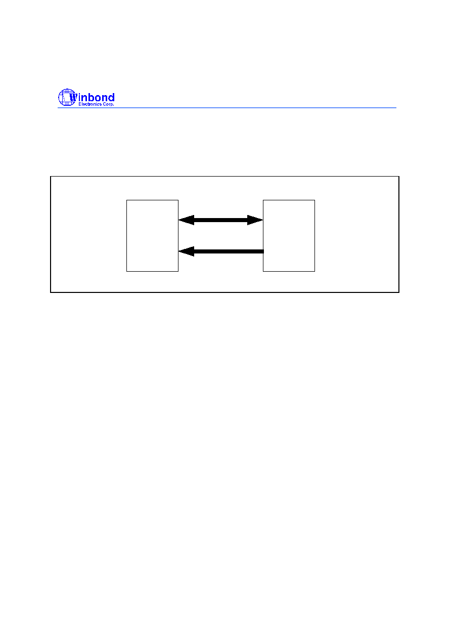
7.4 USB Interface and Device Control
The W9968CF contains two endpoints: default and Video Data-In endpoints. Figure 7.3 shows the
device configuration for the W9968CF-based USB digital video camera.
Host
Device
Default Pipe
Data-In Pipe
W9967CF-Based
Figure 7.3 Device Configuration
7.4.1 Endpoints
7.4.1.1 Default Endpoint (Endpoint 0)
The default endpoint uses control transfers as defined in the USB specification. The default endpoint
provides access to the W9968CF-based device
s configuration, status, and control information by
sending standard, class, and vendor-specific requests to the device, an interface, or an endpoint.
7.4.1.2 Video Data-In Endpoint (Endpoint 1)
The Video Data-In endpoint is used to receive video image data from the device intended for delivery to
a video capture application on the host. The Video Data-In endpoint uses isochronous transfers. The
direction is always IN. The maximum packet size can be varied for different alternate settings for limited
USB bandwidth.
7.4.2 USB Device Requests
The W9968CF responds to requests from the host on the default pipe. The W9968CF supports
standard, class, and vendor-specific USB device requests.
7.4.2.1 Standard Device Requests
The W9968CF supports the standard USB device requests as shown in Table 7.3 and described below.
It responds to standard device requests whether it has been assigned a non-default address or is
currently configured. If any unrecognized or unsupported standard request is received, it returns
STALL.

W9968CF
- 28 -
Table 7.3 Standard Device Requests
bmRequestType
bRequest
wValue
wIndex
wLength
Data
00000010B
CLEAR_FEATURE (1)
Feature
Selector
(0)
Endpoint
Zero
None
10000000B
GET_CONFIGURATION (8)
Zero
Zero
One
Configurati-
on Value
10000000B
GET_DESCRIPTOR (6)
Descriptor
Type and
Descriptor
Index
Zero or
Language
ID
Descriptor
Length
Descriptor
10000001B
GET_INTERFACE (10)
Zero
Interface
(0)
One
Alternate
Setting
10000000B
10000001B
10000010B
GET_STATUS (0)
Zero
Zero
Interface
Endpoint
Two
Device,
Interface,
or Endpoint
Status
00000000B
SET_ADDRESS (5)
Device
Address
Zero
Zero
None
00000000B
SET_CONFIGURATION (9)
Configura
-tion
Value
Zero
Zero
None
00000000B
SET_DESCRIPTOR (7)
(Not Supported)
00000010B
SET_FEATURE (3)
Feature
Selector
(0)
Endpoint
Zero
None
00000001B
SET_INTERFACE (11)
Alternate
Setting
Interface
(0)
Zero
None
00000010B
SYNCH_FRAME (12)
(Not Supported)
Clear Feature
The W9968CF supports the following Clear Feature request:
�
When directed to an endpoint recipient for ENDPOINT_STALL
The W9968CF returns STALL if any unrecognized or unsupported Clear Feature request is received.
Get Configuration
The W9968CF returns zero if it is unconfigured or the bConfiguration value
defined in the Configuration Descriptor is configured.
Get Descriptor
The W9968CF supports Get Descriptor requests for standard descriptors (Device,
Configuration, and String). The W9968CF returns STALL if a Get Descriptor request is received for a
class-specific descriptor or a vendor-specific descriptor, is unrecognized or unsupported.

W9968CF
Publication Release Date: May 1999
- 29 - Revision A2
Get Interface
The W9968CF supports a Get Interface request for Interface 0 by returning the
selected alternate setting. The default alternate setting is zero. The W9968CF returns STALL for a Get
Interface request for any other Interface or any Get Interface request before the Device is configured.
Get Status
The W9968CF supports a Get Status directed at the device, Interface 0, or any
defined endpoint (default or Video Data-In). The W9968CF returns STALL if a Get Status request is
received for Interface 0 or any defined endpoint before the Device is configured, or if a Get Status
request is received for any unrecognized or unsupported recipient.
Set Address
The W9968CF supports a Set Address request to change the Device Address
from the default address (zero) to a unique address.
Set Configuration
The W9968CF supports Set Configuration requests to set the Device
Configuration to zero (unconfigured) or the bConfiguration value defined in the Configuration Descriptor.
The W9968CF returns STALL if a Set Configuration request is received with any other value.
Set Descriptor
The W9968CF does not support update for any defined Descriptor (Device,
Configuration, Interface, Endpoint, or String). It returns STALL for any Set Descriptor request.
Clear Feature
The W9968CF supports the following Set Feature request:
�
When directed to an endpoint recipient for ENDPOINT_STALL
The W9968CF returns STALL if any unrecognized or unsupported Set Feature request is received.
Set Interface
When configured, the W9968CF supports a Set Interface request to Interface 0
for defined Alternate Settings. This request allows the host to select the desired alternate setting. The
W9968CF returns STALL for any other Set Interface request.
Synch Frame
The W9968CF returns STALL for any Synch Frame request.
7.4.2.2 Video Camera Class-Specific Requests
Currently, there is no class-specific request is defined for the video camera devices. The W9968CF
returns STALL for any class-specific request.
7.4.2.3 Vendor-Specific Requests
The W9968CF supports two vendor-specific requests for the control registers In/Out transfers on the
default pipe (Endpoint 0): Get W9968CF Control and Set W9968CF Control. The vendor-specific
requests defined for the W9968CF are shown in Table 7.4. The W9968CF returns STALL if an
unrecognized or unsupported vendor-specific request is received.
Table 7.4 W9968CF Vendor-Specific Requests
bmRequestType
bRequest
wValue
wIndex
wLength
Data
11000000B
GET_W9968CF_CONTROL (1)
Zero
Index
1
Length
2
Data
01000000B
SET_W9968CF_CONTROL (0)
Data0
3
Index
1
Length
2
Data
Note 1. Index specifies the starting index of the control registers to be accessed. An index counter,

W9968CF
- 30 -
loaded with the Index value, will be incremented by one after every two bytes of data
transferred.
Note 2. Length specifies number of data bytes transferred during the second phase of the control
transfer. It should be an even number value. If this field is zero, there is no data transfer phase.
Note 3. Data0 is a word-sized data to be programmed into the control register indexed by the Index field,
no matter the Length field is zero or not. The internal index counter will be incremented by one
once Data0 is transferred.
Get W9968CF Control
The W9968CF supports a Get W9968CF Control request for W9968CF
control registers IN transfer. Length field should be an even number value. The W9968CF returns
STALL for any unrecognized or unsupported Get W9968CF Control request.
Set W9968CF Control
The W9968CF supports a Set W9968CF Control request for W9968CF
control registers OUT transfer. Length field should be an even number value. If the Length field is zero,
only Data0 is transferred with no data transfer phase. The W9968CF returns STALL for any
unrecognized or unsupported Set W9968CF Control request.
7.4.3 Descriptors
The W9968CF supports the standard USB descriptors as described below. The W9968CF returns
STALL if a request is received for any unrecognized or unsupported standard descriptor.
7.4.3.1 Device Descriptors
The W9968CF returns a Device Descriptor with the values shown in Table 7.5.
Table 7.5 W9968CF Device Descriptor
Offset
Field
Size
Value
Description
0
bLength
1
0x12
Size of this descriptor in bytes
1
bDescriptorType
1
0x01
Device Descriptor Type
2
bcdUSB
2
0x0110
USB Specification Release Number in BCD
4
bDeviceClass
1
0x00
Class code
5
bDeviceSubClass
1
0x00
Subclass code
6
bDeviceProtocol
1
0x00
Protocol code
7
bMaxPacketSize0
1
0x08
Maximum packet size for endpoint zero
8
idVendor
2
0x1046
Vendor ID
10
idProduct
2
0x9967
Product ID
12
bcdDevice
2
0x0110
Device release number in BCD
14
iManufacturer
1
0x01
Index of string descriptor describing
manufacturer
15
iProduct
1
0x02
Index of string descriptor describing product
16
iSerialNumber
1
0x00
Index of string descriptor describing the
device
s serial number

W9968CF
Publication Release Date: May 1999
- 31 - Revision A2
17
bNumConfigurations
1
0x01
Number of possible configurations
Note 1. Vendor ID and Product ID will be replaced with bytes 0-3 of an external serial E
2
PROM or uC if
present.
7.4.3.2 Configuration Descriptors
The W9968CF returns a Configuration Descriptor and other configuration related descriptors as
described below. When the host requests the Configuration Descriptor, all related interface and
endpoint descriptors are returned.
Table 7.6 W9968CF Configuration Descriptor
Offset
Field
Size
Value
Description
0
bLength
1
0x09
Size of this descriptor in bytes
1
bDescriptorType
1
0x02
Configuration Descriptor Type
2
wTotalLength
2
0x0119
Total length of data returned for this
configuration. Includes the combined length of
all descriptors returned for this configuration.
4
bNumberInterfaces
1
0x01
Number of interfaces supported by this
configuration
5
bConfigurationValue
1
0x01
Value used as an argument to Set
Configuration to select this configuration
6
iConfiguration
1
0x00
No configuration string
7
bmAttributes
1
0x80
Configuration characteristics
8
Maxpower
1
0xFA or
0x32
(Note 1)
Maximum power consumption from the bus
when the device is fully operational. Expressed
in 2 mA units.
Note 1. Value of this field is 0xFA (500 mA) for high power devices (CR00_10 = 1), or 0x32 (100 mA)
for low power devices (CR00_10 = 0).
Table 7.7 W9968CF Video Interface Descriptor
Offset
Field
Size
Value
Description
0
bLength
1
0x09
Size of this descriptor in bytes
1
bDescriptorType
1
0x04
Interface Descriptor Type
2
bInterfaceNumber
1
0x00
Number of interface
3
bAlternateSetting
1
0x00
Default alternate setting zero
4
bNumEndpoints
1
0x01
Number of endpoints used by this interface
5
bInterfaceClass
1
0x00
Image interface class code
6
bInterfaceSubClass
1
0x00
Digital Video Camera subclass code
7
bInterfaceProtocol
1
0x00
Protocol code. No class specific protocol.
W9968CF
- 32 -
8
iInterface
1
0x00
No interface string
Table 7.8 W9968CF Data-In Endpoint Descriptor
Offset
Field
Size
Value
Description
0
bLength
1
0x07
Size of this descriptor in bytes
1
bDescriptorType
1
0x05
Endpoint Descriptor Type
2
bEndpointAddress
1
0x81
Endpoint number. Direction is set to IN.
3
bmAttributes
1
0x01
Isochronous transfer type
4
wMaxPacketSize
2
0x00
Default zero bandwidth
6
bInterval
1
0x01
Interval in milliseconds for polling endpoint for
data transfers
The W9968CF Video interface includes 16 alternate settings that allow the Data-In endpoint bandwidth
to be varied decreasingly from 8 Mbps down to 0.5 Mbps in descending 0.5 Mbps steps such that the
device driver can request subsequently smaller bandwidth quantities. A separate interface descriptor
and its associated endpoint are included for each setting. When the host requests the Configuration
Descriptor, all 16 pairs of interface and endpoint descriptors for alternate setting should follow the
interface and endpoint descriptors for the default alternate setting zero.
The W9968CF supports the Get Interface and Set Interface requests to report or select a specific
alternate setting for the Video interface.
Table 7.9 W9968CF Video Interface Alternate Setting 1-16 Interface Descriptor
Offset
Field
Size
Value
Description
0
bLength
1
0x09
Size of this descriptor in bytes
1
bDescriptorType
1
0x04
Interface Descriptor Type
2
bInterfaceNumber
1
0x00
Number of interface
3
bAlternateSetting
1
1-16
(Note 1)
Alternate setting 1-16 for this interface
4
bNumEndpoints
1
0x01
Number of endpoints used by this interface
5
bInterfaceClass
1
0x00
Image interface class code
6
bInterfaceSubClass
1
0x00
Digital Video Camera subclass code
7
bInterfaceProtocol
1
0x00
Protocol code. No class specific protocol.
8
iInterface
1
0x00
No interface string
Note 1. Refer to Table 7.11.
Table 7.10 W9968CF Alternate Setting 1-16 Data-In Endpoint Descriptor
Offset
Field
Size
Value
Description

W9968CF
Publication Release Date: May 1999
- 33 - Revision A2
0
bLength
1
0x07
Size of this descriptor in bytes
1
bDescriptorType
1
0x05
Endpoint Descriptor Type
2
bEndpointAddress
1
0x81
Endpoint number. Direction is set to IN.
3
bmAttributes
1
0x01
Isochronous transfer type
4
wMaxPacketSize
2
Note 1
Maximum packet size of this alternate setting
6
bInterval
1
0x01
Interval in milliseconds for polling endpoint for
data transfers
Note 1. Refer to Table 7.11.
Table 7.11 shows bAlternateSetting fields and wMaxPacketSize fields for these alternate settings.
Table 7.11 The Maximum Data Payload Size in Bytes for Alternate Settings
Alternate Setting
1
2
3
4
5
6
7
8
9
10
11
12
13
14
15
16
bAlternateSetting
1
2
3
4
5
6
7
8
9
10
11
12
13
14
15
16
wMaxPacketSize
1023 959
895
831
767 703 639 575 511 447 383 319 255 191 127 63
7.4.3.3 String Descriptors
The W9968CF includes strings describing the manufacturer and product as shown in Table 7.12.
Table 7.12 W9968CF Default Stream Descriptors
Offset
Field
Size
Value
Description
0
bLength
1
0x04
Length of String descriptor in bytes
1
bDescriptorType
1
0x03
String Descriptor Type
2
bString
2
0x0409
Array of two-byte LangID codes (English
American)
4
bLength
1
0x10
Length of String descriptor in bytes
5
bDescriptorType
1
0x03
String Descriptor Type
6
bString
14
WINBOND
Manufacturer
20
bLength
1
0x10
Length of String descriptor in bytes
21
bDescriptorType
1
0x03
String Descriptor Type
22
bString
14
W9968CF
Product

W9968CF
- 34 -
7.5 Video/Still Image Data Transfer
Video or still image data from the device is delivered to the host system through an isochronous pipe
(Endpoint 1). The maximum packet size can be varied for different alternate settings for limited USB
bandwidth for other USB devices.
7.5.1 Output Video Data Format
The W9968CF supports two video transfer modes: original video transfer mode and JPEG
compression video transfer mode. The captured video stored in the DRAM will be compressed by the
JPEG encoder and then transferred to the host if JPEG compression video transfer mode is selected,
or will be directly transferred to the host if original video transfer mode is selected. Four different
formats are supported for the output video which are selected by bits 1-0 of the Video Capture Control
register (CR26) and bits 1 of the JPEG Encoder Control register (CR39) as described in Table 7.13.
Table 7.13 Output Video Data Format
CR39_1
CR26_1-0
Output Video Data Format
0
00
Original YUV4:2:2 packed mode
0
01
Original YUV4:2:0 packed mode
1
0X
Reserved
1
10
JPEG YUV4:2:2 non-interleaved scan mode
1
11
JPEG YUV4:2:0 non-interleaved scan mode
7.5.2 Video Frame Synchronization
A single video frame typically requires multiple USB packets. One or more zero length isochronous
data packets are used to mark the end of a video frame. The first non-zero data packet is the start of
the next video frame.
If an error is encountered during the reception of a USB packet, the host may discard the entire video
frame. Processing begins again with the next video frame as indicated by the first non-zero length
isochronous data packet after one or more zero-length packet.
7.5.3 Bandwidth Management
The W9968CF provides for varying the bandwidth required by providing a zero-bandwidth interface
(alternate setting zero) and 16 alternate settings interfaces with 8 Mbps down to 0.5 Mbps bandwidth in
descending 0.5 Mbps steps. The default alternate setting zero (with zero bandwidth) selected by a Set
Configuration request allows a video camera to be initially configured even on a highly utilized USB bus.
Before the device begins streaming video data, the host software must select an alternate setting with
the appropriate amount of bandwidth by using the Set Interface request.

W9968CF
Publication Release Date: May 1999
- 35 - Revision A2
7.6 Power Management
The W9968CF provides three output pins as described below for the video camera power management
to meet the USB specification requirements.
�
PWRDWN/PWRDWN#: These pins, when active, are used to turn off the USB 5V power
supply to the video source circuits (CCD/CMOS sensor device, ADC, DSP, video decoder,
etc.).
�
SUSPND: This pin, when active, is used to turn off the 3.3V power supply to the W9968CF
(excluding USBVDD pin, the power supply for the transceiver), DRAM, and E
2
PROM.
Bit 10 of the Miscellaneous Control register (CR00) determines whether the W9968CF-based device is
a high power device or a low power device as described below:
�
CR00_10 = 1: High power, bus-powered devices. They must draw no more than 100 mA
upon power up and may draw up to 500 mA after being configured.
�
CR00_10 = 0: Low power, bus-powered devices. May draw up to 100 mA from their upstream
connection to allow the interface to function when the remainder of the hub is powered down.
7.6.1 W9968CF Reset
The W9968CF has two reset sources: system reset from the input RSTIN# pin, and the USB reset
detected by seeing a single-ended zero (SE0) for more than 2.5 us. All reset sources are joined inside
the W9968CF into a single reset signal which initializes the W9968CF and is also output via the
RSTOUT pin to initialize other external circuits.
Reset can wake the W9968CF from the suspended mode (SUSPND is inactive low) and turn off the
USB 5V power supply to the video source circuits (PWRDWN is active high and PWRDWN# is active
low).
7.6.2 Before Configured
Before configured, the W9968CF should be reset and keep PWRDWN and PWRDWN# to be active
(CR00_4 = 0) such that the W9968CF-based devices will not draw more than 100 mA from the USB
bus power supply. It is required that an external power-on reset should be applied to the RSTIN# pin
before any USB transaction is sent to the W9968CF by the host.
7.6.3 After Configured
After configured, PWRDWN and PWRDWN# pins should be inactive by programming the Camera
Power-on Control register to one (CR00_4 = 1) to enable device functions. The W9968CF-based
devices must draw less than 100 mA (CR00_10 = 0) or 500 mA (CR00_10 = 1) from the bus during
normal operation. The SOF (Start of Frame) packet is guaranteed to occur once a frame to keep full
speed devices awake during normal bus operation.
7.6.4 Suspend
The W9968CF goes into the suspend mode from any powered state when it sees a constant idle state

W9968CF
- 36 -
on the USB bus lines for more than 3.0 ms. When suspended, both SUSPND and PWRDWN are active
high, PWRDWN# is active low, and the Camera Power-on Control register is cleared to zero (CR00_4
= 0). The W9968CF-based devices must draw less than 500 uA from the bus when suspended.
7.6.5 Resume
Once the W9968CF is in the suspended state, it can be resumed by receiving non-idle signaling on the
bus. SUSPND will be inactive low when resumed. PWRDWN and PWRDWN# will remain active until
the Camera Power-on Control register is set to one (CR00_4 = 1) by the host.

W9968CF
Publication Release Date: May 1999
- 37 - Revision A2
7.7 Serial EEPROM Interface
The W9968CF supports an external 1K (128
�
8) serial E
2
PROM as an optional source for IHV-specific
Vendor ID and Product ID. The external E
2
PROM data, in stead of the default data, will be used when a
high is sampled at SDA pin (pin 49) during a reset operation.
7.7.1 EEPROM Data Structure
The E
2
PROM contains IHV-specific Vendor ID and Product ID as described in Table 7.14.
Table 7.14 EEPROM Data Structure
Address
Field
Size
Value
Description
0x00
2
TL
Total length of E
2
PROM data to be returned
0x02
idVendor
2
Vendor ID
0x04
idProduct
2
Product ID
7.7.2 EEPROM Operations
The external E
2
PROM will be only read right after a reset operation. TL (defined in address 0x00) bytes
of data will be read by using a sequential read operation.
START condition: A high-to-low transition of SDA with SCL high is a start condition which must
proceed any other command.
STOP condition: A low-to-high transition of SDA with SCL high is a stop condition which terminates all
communications. After a read sequence, the stop command will place the E
2
PROM in a standby power
mode.
ACKNOWLEDGE: All addresses and data words are serially transmitted to and from the E
2
PROM in
8-bit words. The E
2
PROM will acknowledge by pulling SDA low after receiving each address. The
W9968CF will likewise acknowledge by pulling SDA low after receiving each data word. This must
happen during the ninth clock cycle after each word received and after all other devices have freed the
SDA bus.
Refer to Figure 7.4, a sequential read is initiated by the W9968CF with a start condition followed by a
7-bit data word address (always 0) and a high read bit. The E
2
PROM will respond with an acknowledge
and then serially output 8 data bits. After the W9968CF receives an 8-bit data word, it responds with an
acknowledge. As long as the E
2
PROM receives an acknowledge, it will continue to increment the data
word address and serially clock out sequential data words. The sequential read operation is terminated
when the memory address limit (TL) is reached and the W9968CF does not respond with an
acknowledge but does generate a following stop condition.
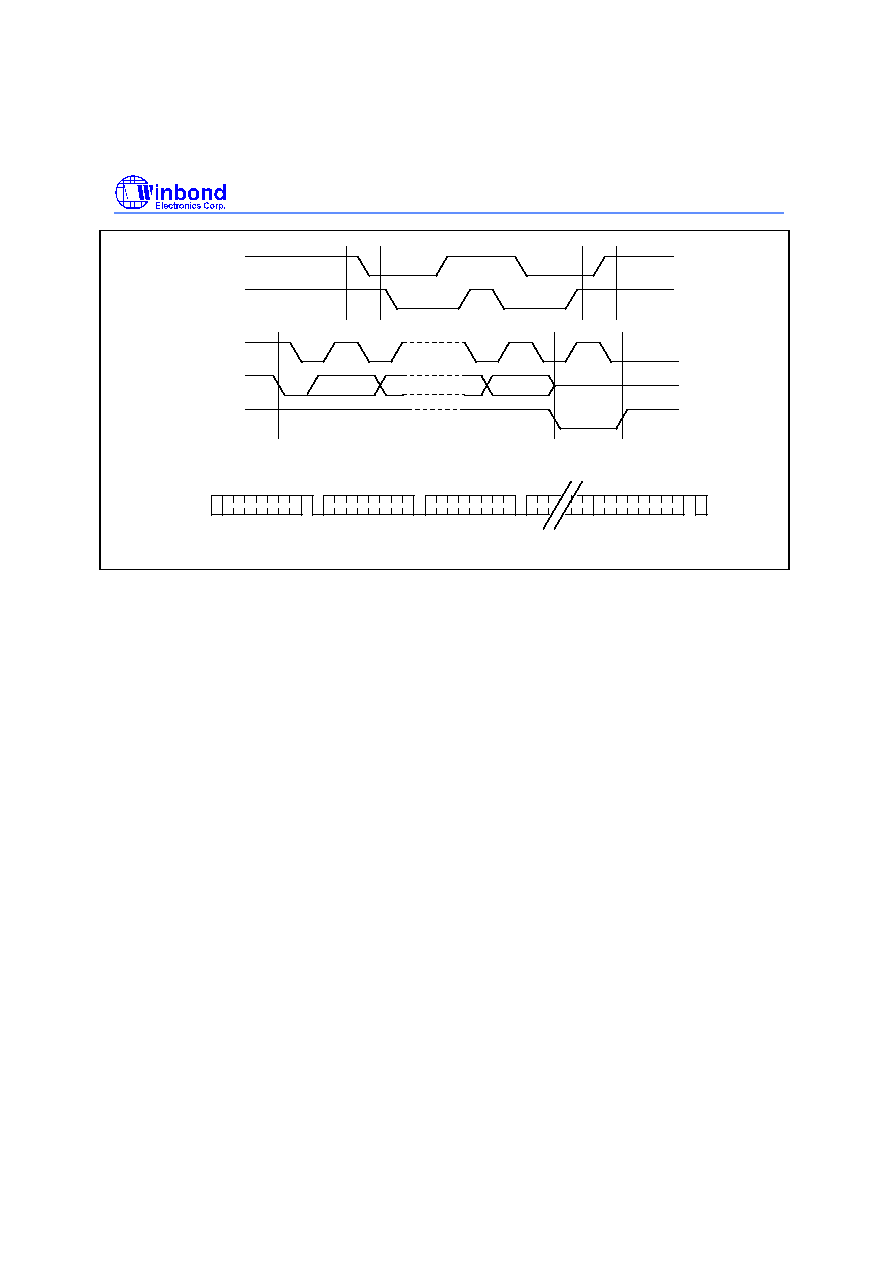
W9968CF
- 38 -
SDA
SCL
START
STOP
ACKNOWLEDGE
1
8
9
START
SCL
SDA IN
SDA OUT
START
MSB
LSB
WORD
ADDRESS (0)
R/W
ACK
DATA 0
ACK
DATA 1
ACK
DATA 127
NO ACK
STOP
SDA
Sequential Read
Figure 7.4 EEPROM Timing Diagram

W9968CF
Publication Release Date: May 1999
- 39 - Revision A2
7.8 Microcontroller Interface
The W9968CF supports an external 8-bit microcontroller to access DRAM and W9968CF internal
registers for portable PC camera applications.
7.8.1 Base Address Setup
The W9968CF internal registers occupy 256-byte microcontroller address space. A special base
address (BA) setup mechanism, described as followed, is designed for the microcontroller to configure
base address for the W9968CF internal register access:
1 assert hardware reset.
2 write the key,
!
!
W
9
9
6
7
!
in ASCII code, to the port xx00H.
3 the port address, xx00H, then will be used as Base Address (BA) for the microcontroller
access.
The setup procedure must be executed right after the hardware reset. Once the procedure is finished,
the xx00H address will be used as the base address until another hardware reset is asserted.
7.8.2 W9968CF Register Access
Since all internal registers are 16-bit wide, it takes two cycles for the microcontroller to access one 16-
bit register through the 8-bit data bus. The two microcontroller access cycles should be in low-byte then
high-byte order. For example, to write CR00 register, the microcontroller must write to BA + 00H
address at first, then write to BA + 01H address to complete this 16-bit register access.
7.8.3 Microcontroller Interrupt
The W9968CF interrupts the microcontroller by forcing INT# pin to low when it completes a still image
capture (original video mode) or JPEG compression of this image (JPEG compression mode). Once
interrupt is acknowledged by the microcontroller, it must write one to bit 5 of the Miscellaneous Control
register (CR00_5) to clear the interrupt. Interrupt can also be disabled by writing zero to bit 6 of the
Miscellaneous Control register (CR00_6).
7.8.4 DRAM Access
The external microcontroller can read/write access DRAM through W9968CF by using the following
registers:
uC Access DRAM Start Address Register (BA + 18H ~ 1AH): specifies the 21-bit starting
WORD address of the DRAM to be accessed.
uC Access DRAM Mode Select (bit 8 of BA + 1BH): specifies read or write access mode.
uC Access DRAM Data Port Register (BA + 1CH ~ 1DH): 16-bit data port which stores data
read from DRAM in read mode, or data to be written into DRAM in write mode.
Read Access (uC reads data from DRAM)

W9968CF
- 40 -
1 DRAM Start Address Setup. Program the 21-bit WORD address to BA + 18H (bits 7-0), BA
+ 19H (bits 15-8), then BA + 1AH (bits 20-16).
2 Read Access Mode Setup. Program 0 to bit 0 of BA + 1BH to select read mode. W9968CF
then starts accessing 16-bit DRAM data into the internal latches, and the internal DRAM
address will be increased by 1 automatically after the access.
3 Read Low-Byte DRAM Data. Read low-byte DRAM data from BA + 1CH location.
4 Read High-Byte DRAM Data. Read high-byte DRAM data from BA + 1DH location. The
W9968CF starts accessing the next-address DRAM data and the internal DRAM address
will be increased by 1 automatically after the access.
5 Read Contiguous DRAM Data. Repeat steps 3 and 4 for contiguous DRAM data
accesses.
Write Access (uC writes data to DRAM)
1 DRAM Start Address Setup. Program the 21-bit WORD address to BA + 18H (bits 7-0), BA
+ 19H (bits 15-8), then BA + 1AH (bits 20-16).
2 Write Access Mode Setup. Program 1 to bit 0 of BA + 1BH to select write mode.
3 Write Low-Byte DRAM Data. Write low-byte DRAM data into BA + 1CH location.
4 Write High-Byte DRAM Data. Write high-byte DRAM data into BA + 1DH location. The
W9968CF then starts writing the 16-bit data into DRAM and the internal DRAM address
will be increased by 1 automatically after the access.
5 Write Contiguous DRAM Data. Repeat steps 3 and 4 for contiguous DRAM data
accesses.
7.8.5 IHV-Specific Information
The microcontroller can provide IHV-specific information including Vendor ID, Product ID, Device
release number, and string descriptors of manufacturer, product, and device
s serial number as that of
E
2
PROM to save the cost of an E
2
PROM. Maximum 128 bytes information can be provided and data
structure is the same as that of E
2
PROM shown in Table 7.14. All IHV-specific information must be
written to the W9968CF via the Vendor String Data Port register (CR0F) in word-aligned sequence right
after hardware reset and base address is set up.

W9968CF
Publication Release Date: May 1999
- 41 - Revision A2
8 CONTROL AND STATUS REGISTERS
The internal W9968CF control registers can be accessed by performing one of the two vendor-specific
requests on the default pipe (Endpoint 0): Get W9968CF Control for read access and Set W9968CF
Control for write access. All W9968CF control registers are 16-bit wide and can be accessed in WORD
only. Table 8.1 shows the control register map.
Table 8.1 W9968CF Control Register Map
Index
uC Address
Symbol
Description
0000H
BA + 00H - 01H
CR00
Miscellaneous Control Register
0001H
BA + 02H - 03H
CR01
Serial Bus Control Register
0002H
BA + 04H - 05H
CR02
General I/O Port Control Register
0003H
BA + 06H - 07H
CR03
DRAM Timing Control Register
0004H
BA + 08H - 09H
CR04
SDRAM Control Register
0005H
BA + 0AH - 0BH
CR05
Memory Controller Test Mode Control Register
0006H
BA + 0CH - 0DH
CR06
Fast Serial Bus Write Register 0
0007H
BA + 0EH - 0FH
CR07
Fast Serial Bus Write Register 1
0008H
BA + 10H - 11H
CR08
Fast Serial Bus Write Register 2
0009H
BA + 12H - 13H
CR09
Fast Serial Bus Write Register 3
000CH
BA + 18H - 19H
CR0C
uC Access DRAM Start Address Low Register
000DH
BA + 1AH - 1BH
CR0D
uC Access DRAM Start Address High Register
000EH
BA + 1CH - 1DH
CR0E
uC Access DRAM Data Port Register
000FH
BA + 1EH - 1FH
CR0F
Vendor String Register
0010H
BA + 20H - 21H
CR10
Cropping Window Start X Register
0011H
BA + 22H - 23H
CR11
Cropping Window Start Y Register
0012H
BA + 24H - 25H
CR12
Cropping Window End X Register
0013H
BA + 26H - 27H
CR13
Cropping Window End Y Register
0014H
BA + 28H - 29H
CR14
Captured Video Width Register
0015H
BA + 2AH - 2BH
CR15
Captured Video Height Register
0016H
BA + 2CH - 2DH
CR16
Video Capture Control Register
0017H
BA + 2EH - 2FH
CR17
Video Capture Test Mode Control Register
0018H
BA + 30H - 31H
CR18
Capture Test Data Register
0020H
BA + 40H - 41H
CR20
Capture Y Frame Buffer 0 Start Address Low Register
0021H
BA + 42H - 43H
CR21
Capture Y Frame Buffer 0 Start Address High Register

W9968CF
- 42 -
0022H
BA + 44H - 45H
CR22
Capture Y Frame Buffer 1 Start Address Low Register
0023H
BA + 46H - 47H
CR23
Capture Y Frame Buffer 1 Start Address High Register
0024H
BA + 48H - 49H
CR24
Capture U Frame Buffer 0 Start Address Low Register
0025H
BA + 4AH - 4BH
CR25
Capture U Frame Buffer 0 Start Address High Register
0026H
BA + 4CH - 4DH
CR26
Capture U Frame Buffer 1 Start Address Low Register
0027H
BA + 4EH - 4FH
CR27
Capture U Frame Buffer 1 Start Address High Register
0028H
BA + 50H - 51H
CR28
Capture V Frame Buffer 0 Start Address Low Register
0029H
BA + 52H - 53H
CR29
Capture V Frame Buffer 0 Start Address High Register
002AH
BA + 54H - 55H
CR2A
Capture V Frame Buffer 1 Start Address Low Register
002BH
BA + 56H - 57H
CR2B
Capture V Frame Buffer 1 Start Address High Register
002CH
BA + 58H - 59H
CR2C
Capture Y Frame Buffer Stride Register
002DH
BA + 5AH - 5BH
CR2D
Capture UV Frame Buffer Stride Register
002EH
BA + 5CH - 5DH
CR2E
Video Capture Y FIFO Threshold Register
002FH
BA + 5EH - 5FH
CR2F
Video Capture UV FIFO Threshold Register
0030H
BA + 60H - 61H
CR30
Image Maximum Width Register
0031H
BA + 62H - 63H
CR31
Image Maximum Height Register
0032H
BA + 64H - 65H
CR32
Compressed Bitstream Buffer 0 Start Address Low Register
0033H
BA + 66H - 67H
CR33
Compressed Bitstream Buffer 0 Start Address High Register
0034H
BA + 68H - 69H
CR34
Compressed Bitstream Buffer 1 Start Address Low Register
0035H
BA + 6AH - 6BH
CR35
Compressed Bitstream Buffer 1 Start Address High Register
0036H
BA + 6CH - 6DH
CR36
Restart Interval Register
0037H
BA + 6EH - 6FH
CR37
VLE FIFO Threshold Register
0038H
BA + 70H - 71H
CR38
Vertical Up-scaling Control Register
0039H
BA + 72H - 73H
CR39
JPEG Encoder Control Register
003AH
BA + 74H - 75H
CR3A
JPEG Image Size Low Register
003BH
BA + 76H - 77H
CR3B
JPEG Image Size High Register
003CH
BA + 78H - 79H
CR3C
USB FIFO Enable and Threshold Register
003DH
BA + 7AH - 7BH
CR3D
USB Isochronous Transfer Size Low Register
003EH
BA + 7CH - 7DH
CR3E
USB Isochronous Transfer Size High Register
003FH
BA + 7EH - 7FH
CR3F
JPEG/MCTL Test Data Register
0040H-5FH
BA + 80H - BFH
CR40-5F
JPEG Luminance Quantization Table Registers
0060H-7FH
BA + C0H - FFH
CR60-7F
JPEG Chrominance Quantization Table Registers

W9968CF
Publication Release Date: May 1999
- 43 - Revision A2
8.1 General Control Registers
Miscellaneous Control Register (CR00)
Read/Write
Index: 0000H
uC Address: 00H - 01H
Power-on Default:
FF00H
15
14
13
12
11
10
9
8
7
6
5
4
3
2
1
0
FS
SUS ISO RCV PLL
BP
Type
MS
24M INTE INTC PWR
R
JR
UR
MR
Bit 15
Force Suspend Mode (It reflects status of the MD7 pin upon reset)
0 = Force suspend mode when suspend mode is enabled (CR00_14 = 1)
1 = Normal operation
Bit 14
Suspend Mode Enable (It reflects status of the MD6 pin upon reset)
0 = Disable
1 = Enable
Bit 13
Isochronous Handshake Phase Support (It reflects status of the MD5 pin upon reset)
0 = Enable
1 = Disable
Bit 12
Differential RCV Source (It reflects status of the MD4 pin upon reset)
0 = Generated by the SIE
1 = Generated by the USB transceiver
Bit 11
PLL Enable (It reflects status of the MD3 pin upon reset)
0 = Disable
1 = Enable
Bit 10
High Power Device (It reflects status of the MD2 pin upon reset)
0 = Low power device
1 = High power device
Bit 9
DRAM Type (It reflects status of the MD1 pin upon reset)
0 = EDO DRAM
1 = SDRAM
Bit 8
DRAM Size (It reflects status of the MD0 pin upon reset)
0 = 256K
�
DRAM

W9968CF
- 44 -
1 = 1M
�
DRAM
Bit 7
CLK24M Output Enable
0 = Disable, CLK24M pin is forced to low
1 = Enable
Bit 6
Interrupt Enable
0 = Disable, INT# is forced to inactive high
1 = Enable
Bit 5
Interrupt Clear
0 = Normal operation
1 = Clear interrupt, INT# will be cleared to high if enabled.
Bit 4
Camera Power-on Control
0 = Power-down
1 = Power-on
Note. This register will be cleared to zero when suspended.
Bit 3
Reserved
Bit 2
JPEG Encoder Reset
0 = Normal operation
1 = Reset JPEG encoder
Bit 1
USB FIFO Reset
0 = Normal operation
1 = Reset USB FIFO
Bit 0
MD Bus Reset
0 = Normal operation
1 = Reset MD bus (tri-stated)
Serial Bus Control Register (CR01)
Read/Write
Index: 0001H
uC Address: 02H - 03H
Power-on Default:
0000H
15
14
13
12
11
10
9
8
7
6
5
4
3
2
1
0
Reserved
EEP MCU XTR
Reserved
FSB SDE SDR SCR SDW SCW
Bits 15-11 Reserved

W9968CF
Publication Release Date: May 1999
- 45 - Revision A2
Bit 10
External EEPROM Enable (Read-only, it reflects status of the SDA pin upon reset)
0 = Disable
1 = Enable
Bit 9
External Microcontroller Enable (Read-only, it reflects status of the EXTMCU pin)
0 = Disable
1 = Enable
Bit 8
USB Transceiver (It reflects status of the INTXTR pin upon reset)
0 = External transceiver
1 = Internal transceiver
Bits 7-6
Reserved
Bit 5
Fast Serial Bus Write Enable
0 = Disable, serial bus outputs (SDATA and SCLK) are controlled by CR01_1-0
1 = Enable, serial bus outputs (SDATA and SCLK) are controlled by CR06 - CR09. Once
CR09 is programmed, all 32-bit data for SDATA and 32-bit data for SCLK from CR06 -
CR09 will be serially output in 400 Khz bit frequency (2.5 us bit time).
Bit 4
Serial Data Enable/Serial Data Strobe
0 = SDE#/SDS pin is driven low
1 = SDE#/SDS pin is driven high
Bit 3
Serial Interface Data Read (Read only)
0 = SDATA is low
1 = SDATA is high
Bit 2
Serial Interface Clock Read (Read only)
0 = SCLK is low
1 = SCLK is high
Bit 1
Serial Interface Data Write
0 = SDATA pin is driven low
1 = SDATA pin is tri-stated
Bit 0
Serial Interface Clock Write
0 = SCLK pin is driven low
1 = SCLK pin is tri-state
General I/O Port Control Register (CR02)
Read/Write
Index: 0002H
uC Address: 04H - 05H

W9968CF
- 46 -
Power-on Default:
0000H
15
14
13
12
11
10
9
8
7
6
5
4
3
2
1
0
P7W P6W P5W P4W P3W P2W P1W P0W P7D P6D P5D P4D P3D P2D P1D P0D
Bits 15-8 GPIO[7:0] Direction
0 = Input
1 = Output
Bits 7-0
GPIO[7:0] Data
0 = Low
1 = High
Note. GPIO[7:0] pins are used as A[15:8] to the external microcontroller if used (EXTMCU = 1). This
register does not control on the GPIO[7:0] pins if an external microcontroller is used.
DRAM Timing Control Register (CR03)
Read/Write
Index: 0003H
uC Address: 06H - 07H
Power-on Default:
405DH
15
14
13
12
11
10
9
8
7
6
5
4
3
2
1
0
R
Refresh Cycles
DCT
T_RP
RAS
T_RCD
T_RAS
RE
T_CAS
Bit 15
Reserved
Bits 14-12 Refresh Cycles
000 = 1 refresh cycle per horizontal scan line
001 = 2 refresh cycles per horizontal scan line
010 = 3 refresh cycles per horizontal scan line
011 = 4 refresh cycles per horizontal scan line
100 = 5 refresh cycles per horizontal scan line
101 = 6 refresh cycles per horizontal scan line
110 = 7 refresh cycles per horizontal scan line
111 = 8 refresh cycles per horizontal scan line
Bit 11
DCT DRAM Data Access
0 = DCT DRAM data access can be interrupted by MCTL when other DRAM request is
active.
1 = DCT DRAM data access cannot be interrupted by MCTL.

W9968CF
Publication Release Date: May 1999
- 47 - Revision A2
Bits 10-9 RAS# Precharge Time Control
00 = 2 MCLKs
01 = 3 MCLKs
10 = 4 MCLKs
11 = 5 MCLKs
Bit 8
RAS# Precharge Time Shrink
0 = Not shrink
1 = Shrink by 0.5 MCLK over that specified by bits 10-9 of this register
Bits 7-6
RAS# Low to CAS# Low Time Control
00 = 1 MCLK
01 = 2 MCLKs
10 = 3 MCLKs
11 = 4 MCLKs
Bits 5-3
Refresh Cycle RAS# Low Pulse Width Control
000 ~ 111 = 1 ~ 8 MCLK cycles
Bit 2
RAS# Low Extend
0 = Not extend
1 = Extend 1 MCLK
Bits 1-0
CAS# Low Stretch Control
00 = Not stretch
01 = Stretch approximately 1 ns
10 = Stretch approximately 2 ns
11 = Stretch approximately 3 ns
SDRAM Control Register (CR04)
Read/Write
Index: 0004H
uC Address: 08H - 09H
Power-on Default:
0030H
15
14
13
12
11
10
9
8
7
6
5
4
3
2
1
0
Reserved
Read Latency
BTyp
Burst Length
Bits 15-7 Reserved
Bits 6-4
Read Latency

W9968CF
- 48 -
000 = Reserved
001 = 1 clock
010 = 2 clocks
011 = 3 clocks
100 ~ 111 = Reserved
Bit 3
Burst Type
0 = Sequential
1 = Interleaved
Bits 2-0
Burst Length
Burst Length
Bits 2-0
Sequential (Bit 3 =0)
Interleaved (Bit 3 = 1)
000
1
1
001
2
2
010
4
4
011
8
8
100
Reserved
Reserved
101
Reserved
Reserved
110
Reserved
Reserved
111
Full Page
Reserved
Memory Controller Test Mode Control Register (CR05)
Read/Write
Index: 0005H
uC Address: 0AH - 0BH
Power-on Default:
0000H
15
14
13
12
11
10
9
8
7
6
5
4
3
2
1
0
Reserved
TEN
HD
SR
Test
R
MTS
Bits 15-8 Reserved
Bit 7
Memory Controller Test Mode Enable
0 = Disable
1 = Enable
Bit 6
DRAM Controller Hold Control
0 = Normal operation
1 = Hold DRAM Controller operation
Bit 5
SDRAM Self Refresh
0 = Disable
1 = Enable
W9968CF
Publication Release Date: May 1999
- 49 - Revision A2
Bit 4
SDRAM Delay Test (used for test mode only)
Bit 3
Reserved
Bits 2-0
Memory Controller Test Mode Select
Fast Serial Bus Write Registers 0~3 (CR06~CR09)
Read/Write
Index: 0006H - 0009H
uC Address: 0CH - 13H
Power-on Default:
0000H
CR06
15
14
13
12
11
10
9
8
7
6
5
4
3
2
1
0
C7
D7
C6
D6
C5
D5
C4
D4
C3
D3
C2
D2
C1
D1
C0
D0
CR07
15
14
13
12
11
10
9
8
7
6
5
4
3
2
1
0
C15
D15
C14
D14
C13
D13
C12
D12
C11
D11
C10
D10
C9
D9
C8
D8
CR08
15
14
13
12
11
10
9
8
7
6
5
4
3
2
1
0
C23
D23
C22
D22
C21
D21
C20
D20
C19
D19
C18
D18
C17
D17
C16
D16
CR09
15
14
13
12
11
10
9
8
7
6
5
4
3
2
1
0
C31
D31
C30
D30
C29
D29
C28
D28
C27
D27
C26
D26
C25
D25
C24
D24
D[31:0]
32-bit data for SDATA output. When fast serial bus is enabled (CR01_5 = 1), D[31:0] will be
output serially from LSB to MSB once CR09 is programmed.
C[31:0]
32-bit data for SCLK output. When fast serial bus is enabled (CR01_5 = 1), C[31:0] will be
output serially from LSB to MSB once CR09 is programmed.
uC Access DRAM Start Address Low Register (CR0C)
Read/Write
Index: 000CH
uC Address: 18H - 19H
Power-on Default:
XXXXH
15
14
13
12
11
10
9
8
7
6
5
4
3
2
1
0
uCA[15:0]
Bits 15-0 uC Access DRAM Start Address Low

W9968CF
- 50 -
A 21-bit value specifies the WORD offset from the start of the frame buffer for the external
microcontroller access. This register contains 16 lower-order bits of the value. Bits 20-16
are located at CR0D_4-0.
uC Access DRAM Start Address High Register (CR0D)
Read/Write
Index: 000DH
uC Address: 1AH - 1BH
Power-on Default:
XXXXH
15
14
13
12
11
10
9
8
7
6
5
4
3
2
1
0
Reserved
R/W
Reserved
uCA[20:16]
Bits 15-9 Reserved
Bit 8
uC Access DRAM Mode
0 = Read mode. uC reads data from DRAM.
1 = Write mode. uC writes data to DRAM.
Bits 7-5
Reserved
Bits 4-0
uCA[20:16]
uC Access DRAM Data Port Register (CR0E)
Read/Write
Index: 000EH
uC Address: 1CH - 1DH
Power-on Default:
XXXXH
15
14
13
12
11
10
9
8
7
6
5
4
3
2
1
0
High Byte Data
Low Byte Data
Bits 15-8 High Byte Data
Bits 7-0
Low Byte Data
Vendor String Data Port Register (CR0F)
Write-only
Index: 000FH
uC Address: 1EH - 1FH
Power-on Default:
XXXXH
15
14
13
12
11
10
9
8
7
6
5
4
3
2
1
0
Vendor String Data Port

W9968CF
Publication Release Date: May 1999
- 51 - Revision A2
Bits 15-0 Vendor String Data Port
Maximum 128 bytes IHV-specific information can be provided by the microcontroller through
this data port. This data port can be written by the microcontroller only and is prohibted from
the USB interface accessing.

W9968CF
- 52 -
8.2 Video Input Control Registers
Cropping Window Start X Register (CR10)
Read/Write
Index: 0010H
uC Address: 20H - 21H
Power-on Default:
XXXXH
15
14
13
12
11
10
9
8
7
6
5
4
3
2
1
0
Reserved
Cropping Window Start X
Bits 15-10 Reserved
Bits 11-0 Cropping Window Start X
A 12-bit value specifies the number of pixels between the inactive edge of HS and the first
cropped video pixel.
Cropping Window Start Y Register (CR11)
Read/Write
Index: 0011H
uC Address: 22H - 23H
Power-on Default:
XXXXH
15
14
13
12
11
10
9
8
7
6
5
4
3
2
1
0
Reserved
Cropping Window Start Y
Bits 15-11 Reserved
Bits 10-0 Cropping Window Start Y
An 11-bit value specifies the number of lines between the inactive edge of VS and the first
cropped video data line.
Cropping Window End X Register (CR12)
Read/Write
Index: 0012H
uC Address: 24H - 25H
Power-on Default:
XXXXH
15
14
13
12
11
10
9
8
7
6
5
4
3
2
1
0
Reserved
Cropping Window End X
W9968CF
Publication Release Date: May 1999
- 53 - Revision A2
Bits 15-12 Reserved
Bits 10-1 Cropping Window End X
A 12-bit value specifies the number of pixels between the inactive edge of HS and the last
cropped video pixel.
Cropping Window End Y Register (CR13)
Read/Write
Index: 0013H
uC Address: 26H - 27H
Power-on Default:
XXXXH
15
14
13
12
11
10
9
8
7
6
5
4
3
2
1
0
Reserved
Cropping Window End Y
Bits 15-11 Reserved
Bits 10-0 Cropping Window End Y
An 11-bit value specifies the number of lines between the inactive edge of VS and the last
cropped video data line.
Captured Video Width Register (CR14)
Read/Write
Index: 0014H
uC Address: 28H - 29H
Power-on Default:
XXXXH
15
14
13
12
11
10
9
8
7
6
5
4
3
2
1
0
Reserved
Captured Video Width
Bits 15-11 Reserved
Bits 10-0 Captured Video Width
An 11-bit value specifies the width in pixel of the captured video which is down-scaled (or
not) from the cropped video. CR14
CR12
-
CR10. Down-scaling is automatically done by
an internal DDA (Digital Differential Accumulator).
Captured Video Height Register (CR15)
Read/Write
Index: 0015H
uC Address: 2AH - 2BH
Power-on Default:
XXXXH
W9968CF
- 54 -
15
14
13
12
11
10
9
8
7
6
5
4
3
2
1
0
Reserved
Captured Video Height
Bits 15-11 Reserved
Bits 10-0 Captured Video Height
An 11-bit value specifies the height in line of the captured video which is down-scaled (or
not) from the cropped video. CR15
CR13
-
CR11. Down-scaling is automatically done by
an internal DDA (Digital Differential Accumulator).
Video Capture Control Register (CR16)
Read/Write
Index: 0016H
uC Address: 2CH - 2DH
Power-on Default:
0000H
15
14
13
12
11
10
9
8
7
6
5
4
3
2
1
0
VCE
CAPCTL
VSP HSP VIM
VI Format
DBE DBS CLM CKF FTE FTM VC Format
Bit 15
Video Capture Enable
0 = Disable
1 = Enable
Bits 14-13 Video Capture Control
00 = Capture all received fields/frames video data
01 = Capture every other received fields/frames video data
10 = Capture and hold after one frame/field (non-interlaced/interlaced mode)
11 = Reserved
Bit 12
VS Input Pin Polarity
0 = Negative sync pulse
1 = Positive sync pulse
Bit 11
HS Input Pin Polarity
0 = Negative sync pulse
1 = Positive sync pulse
Bit 10
Input Video Mode
0 = 16-bit mode
1 = 8-bit mode
Bits 9-8
Input Video Data Format

W9968CF
Publication Release Date: May 1999
- 55 - Revision A2
YUV Input Video Data Format
Bits 9-8
8-bit Mode (Y[7:0])
16-bit Mode (UV[7:0])
00
Y, U, Y, V,
...
U, V, U, V,
...
01
U, Y, V, Y,
...
U, V, U, V,
...
10
Y, V, Y, U,
...
V, U, V, U,
...
11
V, Y, U, Y,
...
V, U, V, U,
...
Bit 7
Double Buffering Enable
0 = Disable
1 = Enable
Bit 6
Double Buffering Status (Read-only)
0 = Buffer 0 active
1 = Buffer 1 active
Bit 5
Video Data Clamping Enable (Clamped to CCIR-601 Format)
0 = Disable
1 = Enable (Y is clamped to 16
-
235, UV is clamped to 16
-
240)
Bit 4
VICLK Falling Edge Latch
0 = Input video data and signals are latched by rising edge of VICLK
1 = Input video data and signals are latched by falling edge of VICLK
Bit 3
Filter Enable
0 = Disable
1 = Enable
Bit 2
Filter Type
0 = 1-2-1 filter
1 = 2-3-6-3-2 filter
Bits 1-0
Captured Video Data Format
00 = YUV4:2:2 packed mode
01 = YUV4:2:0 packed mode
10 = YUV4:2:2 planar mode
11 = YUV4:2:0 planar mode
Video Capture Test Mode Control Register (CR17)
Read/Write
Index: 0017H
uC Address: 2EH - 2FH
Power-on Default:
0000H

W9968CF
- 56 -
15
14
13
12
11
10
9
8
7
6
5
4
3
2
1
0
Reserved
TEN
Reserved
Video Test Selection
Bits 15-8 Reserved
Bit
7
Video Capture Test Mode Enable
0 = Normal operation
1 = Test mode enable
Bits 6-5
Reserved
Bits 4-0
Video Capture Test Mode Selection
Capture Test Data Register (CR18)
Read/Write
Index: 0018H
uC Address: 30H - 31H
Power-on Default:
XXXXH
15
14
13
12
11
10
9
8
7
6
5
4
3
2
1
0
Capture Test Data
Bits 15-0 Capture Test Data (used for test mode only)
Capture Y Frame Buffer 0 Start Address Low Register (CR20)
Read/Write
Index: 0020H
uC Address: 40H - 41H
Power-on Default:
XXXXH
15
14
13
12
11
10
9
8
7
6
5
4
3
2
1
0
CAPYSA0[15:0]
Bits 15-0 Capture Y Frame Buffer 0 Start Address Low
A 21-bit value specifies the WORD offset from the start of the frame buffer for buffer 0
(packed mode), or Y components (planar mode) of the captured video. Buffer 0 is always
used, no matter double buffering is enabled or disabled. This register contains 16 lower-
order bits of the value. Bits 20-16 are located at CR17_4-0.
Capture Y Frame Buffer 0 Start Address High Register (CR21)

W9968CF
Publication Release Date: May 1999
- 57 - Revision A2
Read/Write
Index: 0021H
uC Address: 42H - 43H
Power-on Default:
XXXXH
15
14
13
12
11
10
9
8
7
6
5
4
3
2
1
0
Reserved
CAPYSA0[20:16]
Bits 15-5 Reserved
Bits 4-0
CAPYSA0[20:16]
Capture Y Frame Buffer 1 Start Address Low Register (CR22)
Read/Write
Index: 0022H
uC Address: 44H - 45H
Power-on Default:
XXXXH
15
14
13
12
11
10
9
8
7
6
5
4
3
2
1
0
CAPYSA1[15:0]
Bits 15-0 Capture Y Frame Buffer 1 Start Address Low
A 21-bit value specifies the WORD offset from the start of the frame buffer for buffer 1
(packed mode), or Y components (planar mode) of the captured video. Buffer 1 is not used
if double buffering is disabled. This register contains 16 lower-order bits of the value. Bits
20-16 are located at CR19_4-0.
Capture Y Frame Buffer 1 Start Address High Register (CR23)
Read/Write
Index: 0023H
uC Address: 46H - 47H
Power-on Default:
XXXXH
15
14
13
12
11
10
9
8
7
6
5
4
3
2
1
0
Reserved
CAPYSA1[20:16]
Bits 15-5 Reserved
Bits 4-0
CAPYSA1[20:16]
Capture U Frame Buffer 0 Start Address Low Register (CR24)
Read/Write
Index: 0024H
uC Address: 48H - 49H

W9968CF
- 58 -
Power-on Default:
XXXXH
15
14
13
12
11
10
9
8
7
6
5
4
3
2
1
0
CAPUSA0[15:0]
Bits 15-0 Capture U Frame Buffer 0 Start Address Low
A 21-bit value specifies the WORD offset from the start of the frame buffer for U
components (planar mode) of the captured video. It is not used if the captured video is in
packed mode. Buffer 0 is always used, no matter double buffering is enabled or disabled.
This register contains 16 lower-order bits of the value. Bits 20-16 are located at CR1B_4-0.
Capture U Frame Buffer 0 Start Address High Register (CR25)
Read/Write
Index: 0025H
uC Address: 4AH - 4BH
Power-on Default:
XXXXH
15
14
13
12
11
10
9
8
7
6
5
4
3
2
1
0
Reserved
CAPUSA0[20:16]
Bits 15-5 Reserved
Bits 4-0
CAPUSA0[20:16]
Capture U Frame Buffer 1 Start Address Low Register (CR26)
Read/Write
Index: 0026H
uC Address: 4CH - 4DH
Power-on Default:
XXXXH
15
14
13
12
11
10
9
8
7
6
5
4
3
2
1
0
CAPUSA1[15:0]
Bits 15-0 Capture U Frame Buffer 1 Start Address Low
A 21-bit value specifies the WORD offset from the start of the frame buffer for U
components (planar mode) of the captured video. It is not used if the captured video is in
packed mode. Buffer 1 is not used if double buffering is disabled. This register contains 16
lower-order bits of the value. Bits 20-16 are located at CR1D_4-0.
Capture U Frame Buffer 1 Start Address High Register (CR27)
Read/Write
Index: 0027H
uC Address: 4EH - 4FH

W9968CF
Publication Release Date: May 1999
- 59 - Revision A2
Power-on Default:
XXXXH
15
14
13
12
11
10
9
8
7
6
5
4
3
2
1
0
Reserved
CAPUSA1[20:16]
Bits 15-5 Reserved
Bits 4-0
CAPUSA1[20:16]
Capture V Frame Buffer 0 Start Address Low Register (CR28)
Read/Write
Index: 0028H
uC Address: 50H - 51H
Power-on Default:
XXXXH
15
14
13
12
11
10
9
8
7
6
5
4
3
2
1
0
CAPVSA0[15:0]
Bits 15-0 Capture V Frame Buffer 0 Start Address Low
A 21-bit value specifies the WORD offset from the start of the frame buffer for V
components (planar mode) of the captured video. It is not used if the captured video is in
packed mode. Buffer 0 is always used, no matter double buffering is enabled or disabled.
This register contains 16 lower-order bits of the value. Bits 20-16 are located at CR1F_4-0.
Capture V Frame Buffer 0 Start Address High Register (CR29)
Read/Write
Index: 0029H
uC Address: 52H - 53H
Power-on Default:
XXXXH
15
14
13
12
11
10
9
8
7
6
5
4
3
2
1
0
Reserved
CAPVSA0[20:16]
Bits 15-5 Reserved
Bits 4-0
CAPVSA0[20:16]
Capture V Frame Buffer 1 Start Address Low Register (CR2A)
Read/Write
Index: 002AH
uC Address: 54H - 55H
Power-on Default:
XXXXH

W9968CF
- 60 -
15
14
13
12
11
10
9
8
7
6
5
4
3
2
1
0
CAPVSA1[15:0]
Bits 15-0 Capture V Frame Buffer 1 Start Address Low
A 21-bit value specifies the WORD offset from the start of the frame buffer for V
components (planar mode) of the captured video. It is not used if the captured video is in
packed mode. Buffer 1 is not used if double buffering is disabled. This register contains 16
lower-order bits of the value. Bits 20-16 are located at CR21_4-0.
Capture V Frame Buffer 1 Start Address High Register (CR2B)
Read/Write
Index: 002BH
uC Address: 56H - 57H
Power-on Default:
XXXXH
15
14
13
12
11
10
9
8
7
6
5
4
3
2
1
0
Reserved
CAPVSA1[20:16]
Bits 15-5 Reserved
Bits 4-0
CAPVSA1[20:16]
Capture Y Frame Buffer Stride Register (CR2C)
Read/Write
Index: 002CH
uC Address: 58H - 59H
Power-on Default:
XXXXH
15
14
13
12
11
10
9
8
7
6
5
4
3
2
1
0
Reserved
CAPYS[10:0]
Bits 15-11 Reserved
Bits 10-0 Capture Y Frame Buffer Stride
This register specifies the WORD offset of vertically adjacent pixels (packed mode), or
vertically adjacent Y components of the captured video. It is used for both buffer 0 and
buffer 1.
Capture UV Frame Buffer Stride Register (CR2D)
Read/Write
Index: 002DH
uC Address: 5AH - 5BH
W9968CF
Publication Release Date: May 1999
- 61 - Revision A2
Power-on Default:
XXXXH
15
14
13
12
11
10
9
8
7
6
5
4
3
2
1
0
Reserved
CAPYS[9:0]
Bits 15-10 Reserved
Bits 9-0
Capture UV Frame Buffer Stride
This register specifies the WORD offset of vertically adjacent U or V components of the
captured video which is in planar mode. It is used for both buffer 0 and buffer 1. It is not
used if the captured video is in packed mode.
Video Capture Y FIFO Threshold Register (CR2E)
Read/Write
Index: 002EH
uC Address: 5CH - 5DH
Power-on Default:
0804H
15
14
13
12
11
10
9
8
7
6
5
4
3
2
1
0
Reserved
VCAPY_HT[4:0]
Reserved
VCAPY_LT[4:0]
Bits 15-13 Reserved
Bits 12-8 Video Capture Y FIFO High Threshold
When video capture FIFO (packed mode), or Y FIFO (planar mode) is filled to this threshold,
a request is generated to the DRAM controller for DRAM access. Initial value is 08H.
Bits 7-5
Reserved
Bits 4-0
Video Capture Y FIFO Low Threshold
When video capture FIFO (packed mode), or Y FIFO (planar mode) is fetched to this
threshold by DRAM controller, the FIFO is ready to release DRAM access to other pending
requests. Initial value is 04H.
Video Capture UV FIFO Threshold Register (CR2F)
Read/Write
Index: 002FH
uC Address: 5EH - 5FH
Power-on Default:
8484H
15
14
13
12
11
10
9
8
7
6
5
4
3
2
1
0
VCAPU_HT[3:0]
VCAPU_LT[3:0]
VCAPV_HT[3:0]
VCAPV_LT[3:0]

W9968CF
- 62 -
Bits 15-12 Video Capture U FIFO High Threshold
When video capture U FIFO (planar mode) is filled to this threshold, a request is generated
to the DRAM controller for DRAM access. It is not used if the captured video is in packed
mode. Initial value is 08H.
Bits 11-8 Video Capture U FIFO Low Threshold
When video capture U FIFO (planar mode) is fetched to this threshold by DRAM controller,
the FIFO is ready to release DRAM access to other pending requests. It is not used if the
captured video is in packed mode. Initial value is 04H.
Bits 7-4
Video Capture V FIFO High Threshold
When video capture V FIFO (planar mode) is filled to this threshold, a request is generated
to the DRAM controller for DRAM access. It is not used if the captured video is in packed
mode. Initial value is 08H.
Bits 3-0
Video Capture V FIFO Low Threshold
When video capture V FIFO (planar mode) is fetched to this threshold by DRAM controller,
the FIFO is ready to release DRAM access to other pending requests. It is not used if the
captured video is in packed mode. Initial value is 04H.
W9968CF
Publication Release Date: May 1999
- 63 - Revision A2
8.3 JPEG Encoder Control Registers
Image Maximum Width Register (CR30)
Read/Write
Index: 0030H
uC Address: 60H - 61H
Power-on Default:
XXXXH
15
14
13
12
11
10
9
8
7
6
5
4
3
2
1
0
Reserved
MAXW[10:0]
Bits 15-11 Reserved
Bits 10-0 Image Maximum Width
Image Maximum Height Register (CR31)
Read/Write
Index: 0031H
uC Address: 62H - 63H
Power-on Default:
XXXXH
15
14
13
12
11
10
9
8
7
6
5
4
3
2
1
0
Reserved
MAXH[10:0]
Bits 15-11 Reserved
Bits 10-0 Image Maximum Height
Compressed Bitstream Buffer 0 Start Address Low Register (CR32)
Read/Write
Index: 0032H
uC Address: 64H - 65H
Power-on Default:
XXXXH
15
14
13
12
11
10
9
8
7
6
5
4
3
2
1
0
BSSA0[15:0]
Bits 15-0 Compressed Bitstream Buffer 0 Start Address Low
A 21-bit value specifies the WORD offset from the start of the frame buffer for the
compressed bitstream buffer 0. Bits 20-16 are located at CR33_4-0.

W9968CF
- 64 -
Compressed Bitstream Buffer 0 Start Address High Register (CR33)
Read/Write
Index: 0033H
uC Address: 66H - 67H
Power-on Default:
XXXXH
15
14
13
12
11
10
9
8
7
6
5
4
3
2
1
0
Reserved
BSSA0[20:16]
Bits 15-5 Reserved
Bits 4-0
BSSA0[20:16]
Compressed Bitstream Buffer 1 Start Address Low Register (CR34)
Read/Write
Index: 0034H
uC Address: 68H - 69H
Power-on Default:
XXXXH
15
14
13
12
11
10
9
8
7
6
5
4
3
2
1
0
BSSA1[15:0]
Bits 15-0 Compressed Bitstream Buffer 1 Start Address Low
A 21-bit value specifies the WORD offset from the start of the frame buffer for the
compressed bitstream buffer 1. Bits 20-16 are located at CR35_4-0.
Compressed Bitstream Buffer 1 Start Address High Register (CR35)
Read/Write
Index: 0035H
uC Address: 6AH - 6BH
Power-on Default:
XXXXH
15
14
13
12
11
10
9
8
7
6
5
4
3
2
1
0
Reserved
BSSA1[20:16]
Bits 15-5 Reserved
Bits 4-0
BSSA1[20:16]
Restart Interval Register (CR36)
Read/Write
Index: 0036H
uC Address: 6CH - 6DH

W9968CF
Publication Release Date: May 1999
- 65 - Revision A2
Power-on Default:
0000H
15
14
13
12
11
10
9
8
7
6
5
4
3
2
1
0
Restart Interval
Bits 15-0 Restart Interval
Specifies the number of MCU (Minimum Coded Unit) in the restart interval. Restart interval
processing is disabled if this value is 0.
VLE FIFO Threshold Register (CR37)
Read/Write
Index: 0037H
uC Address: 6EH - 6FH
Power-on Default:
0804H
15
14
13
12
11
10
9
8
7
6
5
4
3
2
1
0
Reserved
VLE_HT[3:0]
Reserved
VLE_LT[3:0]
Bits 15-12 Reserved
Bits 11-8 VLE FIFO High Threshold
When VLE FIFO is filled with JPEG coded bitstream to this threshold, a request is
generated to the DRAM controller for DRAM access. Initial value is 08H.
Bits 7-4
Reserved
Bits 3-0
VLE FIFO Low Threshold
When VLE FIFO is fetched to this threshold by DRAM controller, the FIFO is ready to
release DRAM access to other pending requests. Initial value is 04H.
Vertical Up-scaling Control Register (CR38)
Read/Write
Index: 0038H
uC Address: 70H - 71H
Power-on Default:
0000H
15
14
13
12
11
10
9
8
7
6
5
4
3
2
1
0
EN
Reserved
Vertical Up-scaling Factor
Bit 15
Vertical Up-scaling Enable
0 = Disable
1 = Enable

W9968CF
- 66 -
Bits 14-6 Reserved
Bits 5-0
Vertical Up-scaling Factor
Up-scaling ratio (Scaled Height/Original Height) = 1.x, where x = Vertical Up-scaling
Factor/64. The maximum 2
�
up-scaling will be done if 0 is programmed.
JPEG Encoder Control Register (CR39)
Read/Write
Index: 0039H
uC Address: 72H - 73H
Power-on Default:
0000H
15
14
13
12
11
10
9
8
7
6
5
4
3
2
1
0
Reserved
QRD
Reserved
JCLK Test TEN JEN
R
Bits 15-9 Reserved
Bit 8
JPEG Quantization Table Registers (CR40 ~ CR7F) Read Enable
0 = Disable
1 = Enable
Bits 7-5
Reserved
Bit 4
JPEG Clock Enable (Must be enabled before JPEG Q-table access or encoding)
0 = Disable
1 = Enable
Bit 3
JPEG Test (used for test mode only)
Bit 2
JPEG Test Mode Enable
0 = Disable
1 = Enable
Bit 1
JPEG Encoder Enable
0 = Disable
1 = Enable
Bit 0
Reserved
JPEG Image Size Low Register (CR3A)
Read-only
Index: 003AH
uC Address: 74H - 75H
Power-on Default:
XXXXH
15
14
13
12
11
10
9
8
7
6
5
4
3
2
1
0
W9968CF
Publication Release Date: May 1999
- 67 - Revision A2
JIMG_SIZE[15:0]
Bits 15-0 JPEG Image Size Low
A 21-bit value specifies the JPEG compressed image size in WORD. It is used by the
microcontroller to determine starting address for the next still image. This register contains
the 16 lower-order bits of the value. Bits 20-16 are located at CR3B_4-0.
JPEG Image Size High Register (CR3B)
Read-only
Index: 003BH
uC Address: 76H - 77H
Power-on Default:
XXXXH
15
14
13
12
11
10
9
8
7
6
5
4
3
2
1
0
Reserved
JIMG_SIZE _SIZE[20:16]
Bits 15-5 Reserved
Bits 4-0
JPEG Image Size High
This register contains the 4 high-order bits of the JPEG Image Size.
USB FIFO Enable and Threshold Register (CR3C)
Read/Write
Index: 003CH
uC Address: 78H - 79H
Power-on Default:
0A05H
15
14
13
12
11
10
9
8
7
6
5
4
3
2
1
0
UEN
Reserved
USB_HT[3:0]
Reserved
USB_LT[3:0]
Bit 15
USB Isochronous Pipe Transfer Enable
0 = Disable
1 = Enable
Bits 14-12 Reserved
Bits 11-8 USB FIFO High Threshold
Bits 7-4
Reserved
Bits 3-0
USB FIFO Low Threshold

W9968CF
- 68 -
USB Isochronous Transfer Size Low Register (CR3D)
Read/Write
Index: 003DH
uC Address: 7AH - 7BH
Power-on Default:
XXXXH
15
14
13
12
11
10
9
8
7
6
5
4
3
2
1
0
ISO_SIZE[15:0]
Bits 15-0 USB Isochronous Transfer Size Low
A 21-bit value specifies the USB Isochronous Transfer Size in WORD for the original video
transfer or the still image transfer. It is not used for the JPEG compression video transfer
mode (CR39_1 = 1). This register contains the 16 lower-order bits of the value. Bits 20-16
are located at CR3E_4-0.
USB Isochronous Transfer Size High Register (CR3E)
Read/Write
Index: 003EH
uC Address: 7CH - 7DH
Power-on Default:
XXXXH
15
14
13
12
11
10
9
8
7
6
5
4
3
2
1
0
Reserved
ISO_SIZE[20:16]
Bits 15-5 Reserved
Bits 4-0
USB Isochronous Transfer Size High
This register contains the 4 high-order bits of the USB Isochronous Transfer Size. It is not
used for the JPEG compression video transfer mode (CR39_1 = 1).
JPEG/MCTL Test Data Register (CR3F)
Read/Write
Index: 003FH
uC Address: 7EH - 7FH
Power-on Default:
XXXXH
15
14
13
12
11
10
9
8
7
6
5
4
3
2
1
0
JPEG/MCTL Test Data
Bits 15-0 JPEG/MCTL Test Data (used for test mode only)
JPEG Luminance Quantization Table Registers (CR40 -- CR5F)

W9968CF
Publication Release Date: May 1999
- 69 - Revision A2
Read/Write
Index: 0040H - 005FH
uC Address: 80H - BFH
Power-on Default:
XXXXH
15
14
13
12
11
10
9
8
7
6
5
4
3
2
1
0
JPEG Luminance Quantization Table
Bits 15-0 JPEG Luminance Quantization Table
Note. These registers can be read only when CR39 bit 8 is enabled (CR39_8 = 1).
JPEG Chrominance Quantization Table Registers (CR60 -- CR7F)
Read/Write
Index: 0060H - 007FH
uC Address: C0H - FFH
Power-on Default:
XXXXH
15
14
13
12
11
10
9
8
7
6
5
4
3
2
1
0
JPEG Chrominance Quantization Table
Bits 15-0 JPEG Chrominance Quantization Table
Note. These registers can be read only when CR39 bit 8 is enabled (CR39_8 = 1).

W9968CF
- 70 -
9 ELECTRICAL CHARACTERISTICS
9.1 Absolute Maximum Ratings
Table 9.1 Absolute Maximum Ratings
Ambient temperature
0
�
C to 70
�
C
Storage temperature
-40
�
C to 125
�
C
DC supply voltage
-0.5V to 7V
I/O pin voltage with respect to VSS
-0.5V to VDD + 0.5V
9.2 DC Characteristics
9.2.1 USB Transceiver DC Characteristics
Table 9.2 USB Transceiver DC Characteristics
Symbol
Parameter
Conditions
Min.
Max.
Unit
V
DI
Differential Input Sensitivity
DP
-
DM
0.2
V
V
CM
Differential Common Mode Range
Includes V
DI
range
0.8
2.5
V
V
SE
Single Ended Receiver Threshold
0.8
2.0
V
V
OL
Static Output Low Voltage
RL of 1.5 K
to 3.6 V
0.3
V
V
OH
Static Output High Voltage
RL of 15 K
to VSS
2.8
3.6
V
V
CRS
Output Signal Crossover Voltage
1.3
2.0
V
Z
DRV
Driver Output Resistance
Steady state drive
28
43
C
IN
Pin Capacitance
20
pF
9.2.2 Digital DC Characteristics
Table 9.3 Digital DC Characteristics
Symbol
Parameter
Conditions
Min.
Max.
Unit
VDD5V
5V Power Supply
4.40
5.25
V
VDD
3.3V Power Supply
3.0
3.6
V
V
IL
Input Low Voltage
-0.5
0.8
V
V
IH
Input High Voltage
2.0
V
V
OL
Output Low Voltage
VSS+0.4
V
V
OH
Output High Voltage
2.4
V

W9968CF
Publication Release Date: May 1999
- 71 - Revision A2
I
IL
Input Low Leakage Current
V
IN
= 0.4V
+70
�
A
I
IH
Input High Leakage Current
V
IN
= 2.4V
-70
�
A
I
UP
Pull-up Current
V
IN
= 0V
-133.2
-400.6
�
A
C
IO
Pin Capacitance
10
pF
I
PD
Powerdown Current USB
Suspend
200
�
A
I
DD
Active Current
F
CLK
= 12 MHz
120
mA
9.3 AC Characteristics
9.3.1 USB Transceiver AC Characteristics
Low Speed: 75ns at C
L
= 50pF, 300ns at C
L
= 350pF
Full Speed: 4 to 20ns at C
L
= 50pF
Differential
Data Lines
10%
Rise Time
90%
Fall Time
t
F
t
R
10%
90%
C
L
C
L
Figure 9.1 Data Signal Rise and Fall Time
T
PERIOD
Differential
Data Lines
Crossover
Points
Paired
Transitions
N * T
PERIOD
+ T
xJR2
Consecutive
Transitions
N * T
PERIOD
+ T
xJR1
Figure 9.2 Differential Data Jitter
T
PERIOD
Differential
Data Lines
Crossover
Point
Crossover
Point Extended
Source EOP Width:
T
EOPT
Receiver EOP Width: T
EOPR1
, T
EOPR2
Diff. Data to
SE0 Skew
N * T
PERIOD
+ T
DEOP
Figure 9.3 Differential to EOP Transition Skew and EOP Width

W9968CF
- 72 -
Differential
Data Lines
Paired
Transitions
N * T
PERIOD
+ T
JR2
T
PERIOD
Consecutive
Transitions
N * T
PERIOD
+ T
JR1
T
JR
T
JR1
T
JR2
Figure 9.4 Receiver Jitter Tolerance
Table 9.4 USB Transceiver AC Characteristics
Symbol
Parameter
Conditions
Min.
Max.
Unit
T
R
Rise Time
CL = 50 pF
4
20
ns
T
F
Fall Time
CL = 50 pF
4
20
ns
T
RFM
Rise/Fall Time Matching
90
110
%
T
DRATE
Full Speed Data Rate
Average bit rate
(12 Mb/s
�
0.25%)
11.97
12.03
Mbps
T
DJ1
T
DJ2
Source Differential Driver Jitter
To Next Transition
For Paired Transitions
-3.5
-4.0
3.5
4.0
ns
ns
T
EOPT
Source EOP Width
160
175
ns
T
DEOP
Differential to EOP Transition Skew
-2
5
ns
T
JR1
T
JR2
Receiver Data Jitter Tolerance
To Next Transition
For Paired Transitions
-18.5
-9
18.5
9
ns
ns
T
EOPR1
T
EOPR2
EOP Width at Receiver
Must Reject as EOP
Must Accept as EOP
40
82
ns
ns
9.3.2 RESET Timing AC Characteristics
RSTIN#
T
RST
Figure 9.5 RESET Timing

W9968CF
Publication Release Date: May 1999
- 73 - Revision A2
Table 9.5 RESET Timing
Symbol
Parameter
Conditions
Min.
Max.
Unit
T
RST
Reset Pulse Width
100
ns
9.3.3 Clock AC Characteristics
T
HIGH
T
LOW
T
CYC
0.8 V
1.5 V
2.0 V
Figure 9.6 Clock Waveform
Table 9.6 Clock AC Characteristics
Symbol
Parameter
Conditions
Min.
Max.
Unit
1/T
CYC
Oscillator Frequency
VICLK Frequency
SMCLK Frequency
11.988
5
47.88
12.012
30
48.12
MHz
MHz
MHz
T
HIGH
Oscillator Clock High Time
VICLK Clock High Time
SMCLK Clock High Time
33
5
8.3
50
12.5
ns
ns
ns
T
LOW
Oscillator Clock Low Time
VICLK Clock Low Time
SMCLK Clock Low Time
33
5
8.3
50
12.5
ns
ns
ns
9.3.4 Input Video AC Characteristics
VICLK
Y[7:0],
UV[7:0]
HS, VS
T
SU
T
H
1.5 V
1.5 V
1.5 V
input valid
Figure 9.7 Input Video Timing

W9968CF
- 74 -
Table 9.7 Input Video AC Characteristics
Symbol
Parameter
Conditions
Min.
Max.
Unit
T
SU
Y[7:0], UV[7:0], HS, VS Setup Time
6
ns
T
H
Y[7:0], UV[7:0], HS, VS Hold Time
4
ns
9.3.5 DRAM Interface AC Characteristics
SMCLK
MD[15:0]
T
SU
T
H
1.5 V
1.5 V
1.5 V
input valid
Figure 9.8 DRAM Interface Input Timing
SMCLK
OUTPUT
DELAY
T
VAL
1.5 V
1.5 V
Figure 9.9 DRAM Interface Output Timing
Table 9.8 DRAM Interface AC Characteristics
Symbol
Parameter
Conditions
Min.
Max.
Unit
T
SU
MD[15:0] Setup Time
0
ns
T
H
MD[15:0] Hold Time
7
ns
T
H
MD[15:0], MA[10:0], BA,
RAS[1:0]#/CS[1:0]#,
CAS[1:0]#/DQM[1:0], OE#/CKE,
WE#, SRAS#, SCAS#
2
7
ns
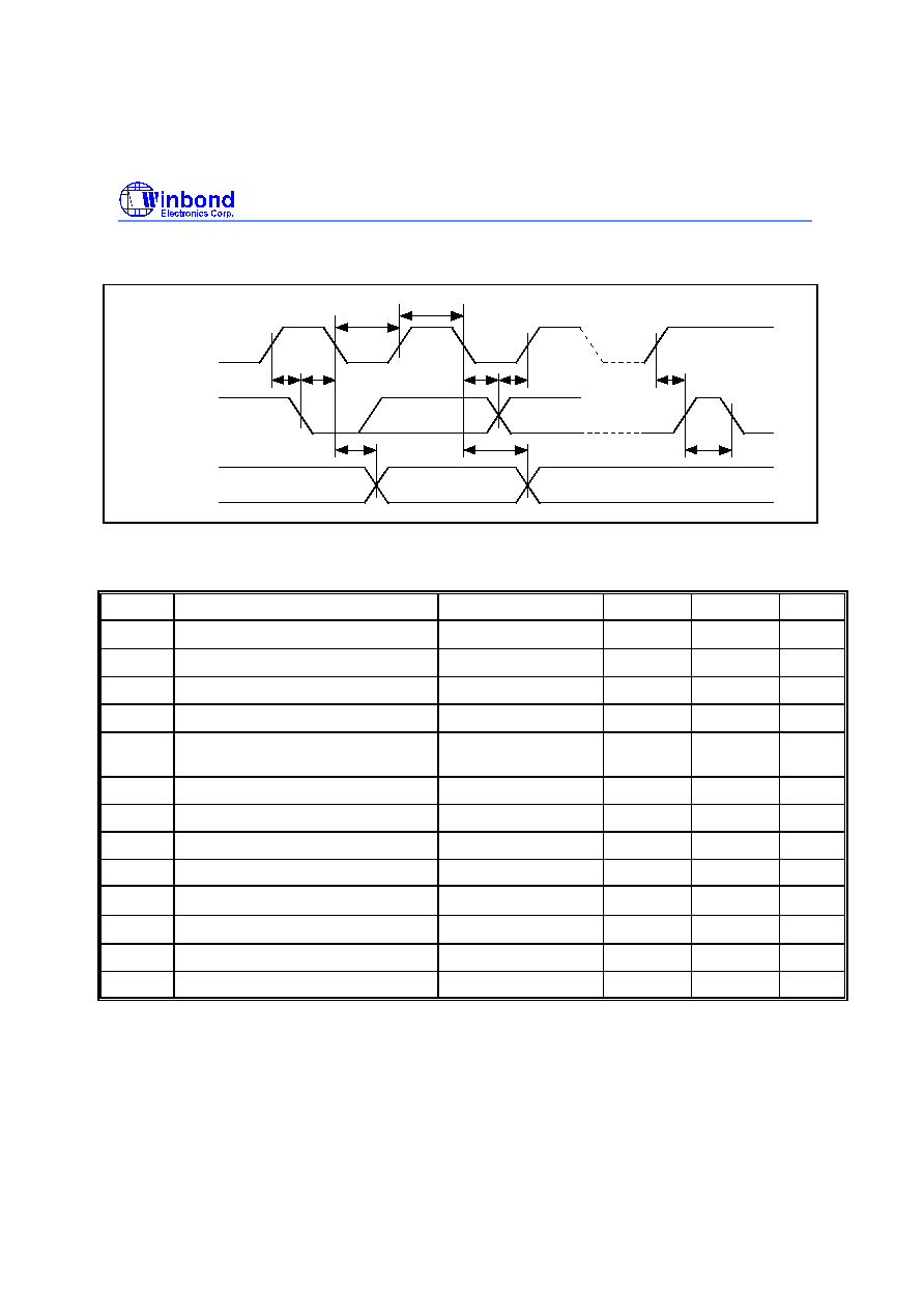
W9968CF
Publication Release Date: May 1999
- 75 - Revision A2
9.3.6 EEPROM Interface AC Characteristics
SCL
SDA IN
T
SU.STA
T
LOW
T
HD.STA
T
HIGH
T
AA
T
DH
T
HD.DAT
T
SU.DAT
SDA OUT
T
BUF
T
SU.STO
Figure 9.10 EEPROM Interface Timing
Table 9.9 EEPROM Interface AC Characteristics
Symbol
Parameter
Conditions
Min.
Max.
Unit
F
SCL
SCL Clock Frequency
100
KHz
T
LOW
Clock Pulse Width Low
4.7
�
s
T
HIGH
Clock Pulse Width High
4.0
�
s
T
AA
Clock Low to Data Out Valid
0.1
4.5
�
s
T
BUF
Time the bus must be free before a
new transmission can start
4.7
�
s
T
HD.STA
Start Hold Time
4.0
�
s
T
SU.STA
Start Set-up Time
4.7
�
s
T
HD.DAT
Data In Hold Time
0
�
s
T
SU.DAT
Data In Set-up Time
200
ns
T
R
Inputs Rise Time
1.0
�
s
T
F
Inputs Fall Time
300
ns
T
SU.STO
Stop Set-up Time
4.7
�
s
T
DH
Data Out Hold Time
100
ns

W9968CF
- 76 -
9.3.7 Microcontroller Interface AC Characteristics
ALE
A[15:8]
AD[7:0]
RD#
AD[7:0]
WR#
A[7:0]
D[7:0]
A[7:0]
D[7:0]
T
AS
T
AH
T
DAR
T
DDA
T
RDH
T
RD
T
DAW
T
WDH
T
WR
Figure 9.11 Microcontroller Interface Timing
Table 9.10 Microcontroller Interface AC Characteristics
Symbol
Parameter
Conditions
Min.
Max.
Unit
T
AS
Address Set-up Time
5
ns
T
AH
Address Hold Time
5
ns
T
DAR
ALE Low to RD# Low
10
ns
T
DDA
RD# Low to Data Valid
T
MCLK
+ 5
ns
T
RDH
Read Data Hold Time
3
ns
T
RD
RD# Pulse Width
2 T
MCLK
ns
T
DAW
ALE Low to WR# Low
10
ns
T
WDH
Write Data Hold Time
5
ns
T
WR
WR# Pulse Width
2 T
MCLK
ns
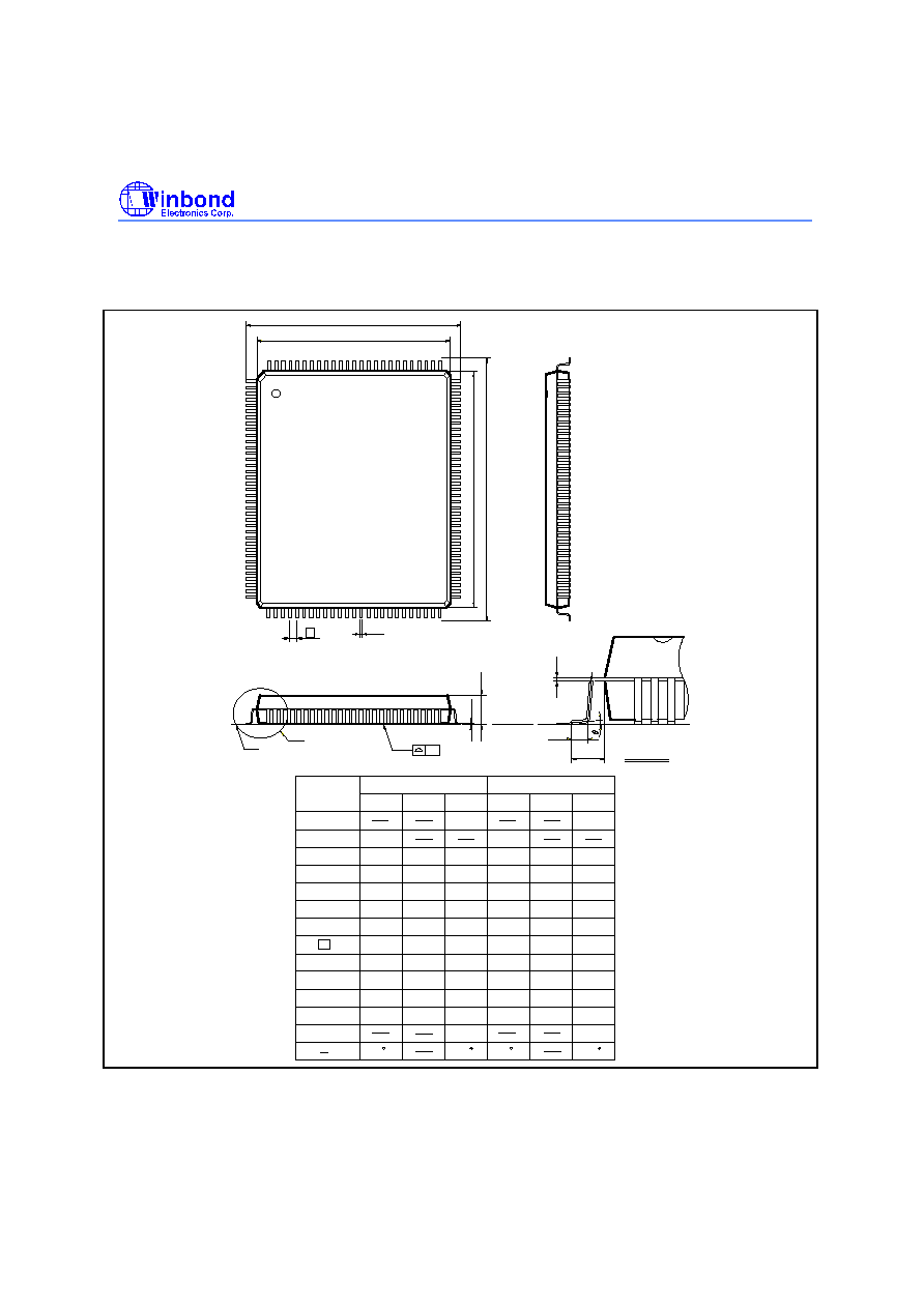
W9968CF
Publication Release Date: May 1999
- 77 - Revision A2
10 PACKAGE SPEC.
0.10
0
12
0
0.004
1.60
1.00
17.40
0.80
17.20
0.60
17.00
0.063
0.039
0.685
0.031
0.677
0.023
0.669
0.50
14.10
0.25
0.25
2.87
3.40
14.00
2.72
13.90
0.10
0.15
2.57
0.10
0.555
0.010
0.010
0.113
0.134
0.551
0.107
0.020
0.547
0.004
0.006
0.101
0.004
Symbol
Min
Nom
Max
Max
Nom
Min
Dimension in inch
Dimension in mm
A
b
c
D
e
H
D
H
E
L
y
0
A
A
L
1
1
2
E
0.008
0.006
0.15
0.20
12
0.783
0.787
0.791
19.90
20.00
20.10
0.905
0.913
0.921
23.00
23.20
23.40
0.055
0.071
1.40
1.80
103
128
102
65
64
39
38
1
c
Detail F
See Detail F
1
L
L
Seating Plane
1
A
A
y
E
H
E
D
D
H
b
e
A
2
Figure 10.1 128L QFP (14x20x2.75mm footprint 3.2mm) Dimensions

W9968CF
- 78 -
11 ORDERING INFORMATION
Part Number
Package
W9968CF
128L QFP
Headquarters
No. 4, Creation Rd. III,
Science-Based Industrial Park,
Hsinchu, Taiwan
TEL: 886-3-5770066
FAX: 886-3-5792647
http://www.winbond.com.tw/
Voice & Fax-on-demand: 886-2-7197006
Taipei Office
11F, No. 115, Sec. 3, Min-Sheng East Rd.,
Taipei, Taiwan
TEL: 886-2-7190505
FAX: 886-2-7197502
Winbond Electronics (H.K.) Ltd.
Rm. 803, World Trade Square, Tower II,
123 Hoi Bun Rd., Kwun Tong,
Kowloon, Hong Kong
TEL: 852-27513100
FAX: 852-27552064
Winbond Electronics North America Corp.
Winbond Memory Lab.
Winbond Microelectronics Corp.
Winbond Systems Lab.
2730 Orchard Parkway, San Jose,
CA 95134, U.S.A.
TEL: 1-408-9436666
FAX: 1-408-9436668
Note: All data and specifications are subject to change without notice.