Document Outline
- WM8736
- 24-bit, 96kHz 6-Channel DAC with Volume Control
- Production Data, January 2001, Rev 2.1
- DESCRIPTION
- FEATURES
- APPLICATIONS
- BLOCK DIAGRAM
- PIN CONFIGURATION
- ORDERING INFORMATION
- ABSOLUTE MAXIMUM RATINGS
- RECOMMENDED OPERATING CONDITIONS
- ELECTRICAL CHARACTERISTICS
- PIN DESCRIPTION
- DEVICE DESCRIPTION
- SYSTEM CLOCK
- AUDIO DATA INTERFACE
- MODES OF OPERATION
- HARDWARE CONTROL MODES
- SOFTWARE CONTROL INTERFACE
- REGISTER MAP
- RECOMMENDED EXTERNAL COMPONENTS
- RECOMMENDED EXTERNAL COMPONENTS VALUES
- APPLICATIONS RECOMMENDED
- PACKAGE DIMENSIONS

WM8736
24-bit, 96kHz 6-Channel DAC with Volume Control
Production Data, January 2001, Rev 2.1
WOLFSON MICROELECTRONICS LTD
Lutton Court, Bernard Terrace, Edinburgh, EH8 9NX, UK
Tel: +44 (0) 131 667 9386
Fax: +44 (0) 131 667 5176
Email: sales@wolfson.co.uk
www.wolfsonmicro.com
Production Data Datasheets contain final
specifications current on publication date.
Supply of products conforms to Wolfson
Microelectronics' Terms and Conditions.
2001 Wolfson Microelectronics Ltd
.
DESCRIPTION
The WM8736 is a high performance 6-channel DAC
designed for audio applications such as DVD, home theatre
systems, and digital TV. The WM8736 supports data input
word lengths from 16 to 24-bits and sampling rates up to
96kHz. The WM8736 consists of a serial interface port,
digital interpolation filters, multi-bit sigma delta modulators
and 6 DACs in a small 28-pin SSOP package. The
WM8736 also includes a digitally controllable mute and
attenuator function on each channel.
The WM8736 supports a variety of connection schemes for
audio DAC control. The SPI-compatible serial port provides
access to a wide range of features including on-chip mute,
attenuation and phase reversal. A hardware controllable
interface is also available.
The WM8736 is an ideal device to interface to AC-3
,
DTS
, and MPEG audio decoders for surround sound
applications.
FEATURES
�
6-channel
DAC
�
Performance:
-
102dB SNR (`A' weighted @ 48kHz), THD+N: -95dB
at full scale
�
5V or 3.3V supply operation
�
Sampling frequency: 8kHz to 96kHz
�
Input data word: 16 to 24-bit
�
Hardware or SPI compatible serial port control modes:
-
Hardware mode: system clock, reset, mute
-
Serial control mode: mute, de-emphasis, digital
attenuation (256 steps), zero mute, power down
APPLICATIONS
�
DVD
�
Home theatre systems
�
Digital
TV
�
Digital broadcast receivers
BLOCK DIAGRAM
SERIAL
INTERFACE
MUTE/
ATTEN
SIGMA
DELTA
MODULATOR
BCKIN (3)
LRCIN (4)
(1)
DVDD
(28)
AVDD2
(16)
CAP
ML/I2S
(12)
RSTB
(10)
MD/DM
(14)
MODE
(8)
MC/IWL
(13)
MUTE
(9)
(11)
DGND
MUTE/
ATTEN
SIGMA
DELTA
MODULATOR
(17) OUT2L
(19) OUT2R
MUTE/
ATTEN
SIGMA
DELTA
MODULATOR
STEREO
DAC
DIGITAL
FILTERS
SCKI
(2)
256fs/384fs/512fs
DIN0 (5)
DIN1 (6)
DIN2 (7)
(20)
AGND1
(24)
AGND2
(18) GR2
(21) OUT1L
(23) OUT1R
(22) GR1
STEREO
DAC
(25) OUT0L
(27) OUT0R
(26) GR0
STEREO
DAC
CONTROL INTERFACE
(15)
AVDD1
WM8736
WM8736
Production Data
WOLFSON MICROELECTRONICS LTD
PD Rev 2.1 January 2001
2
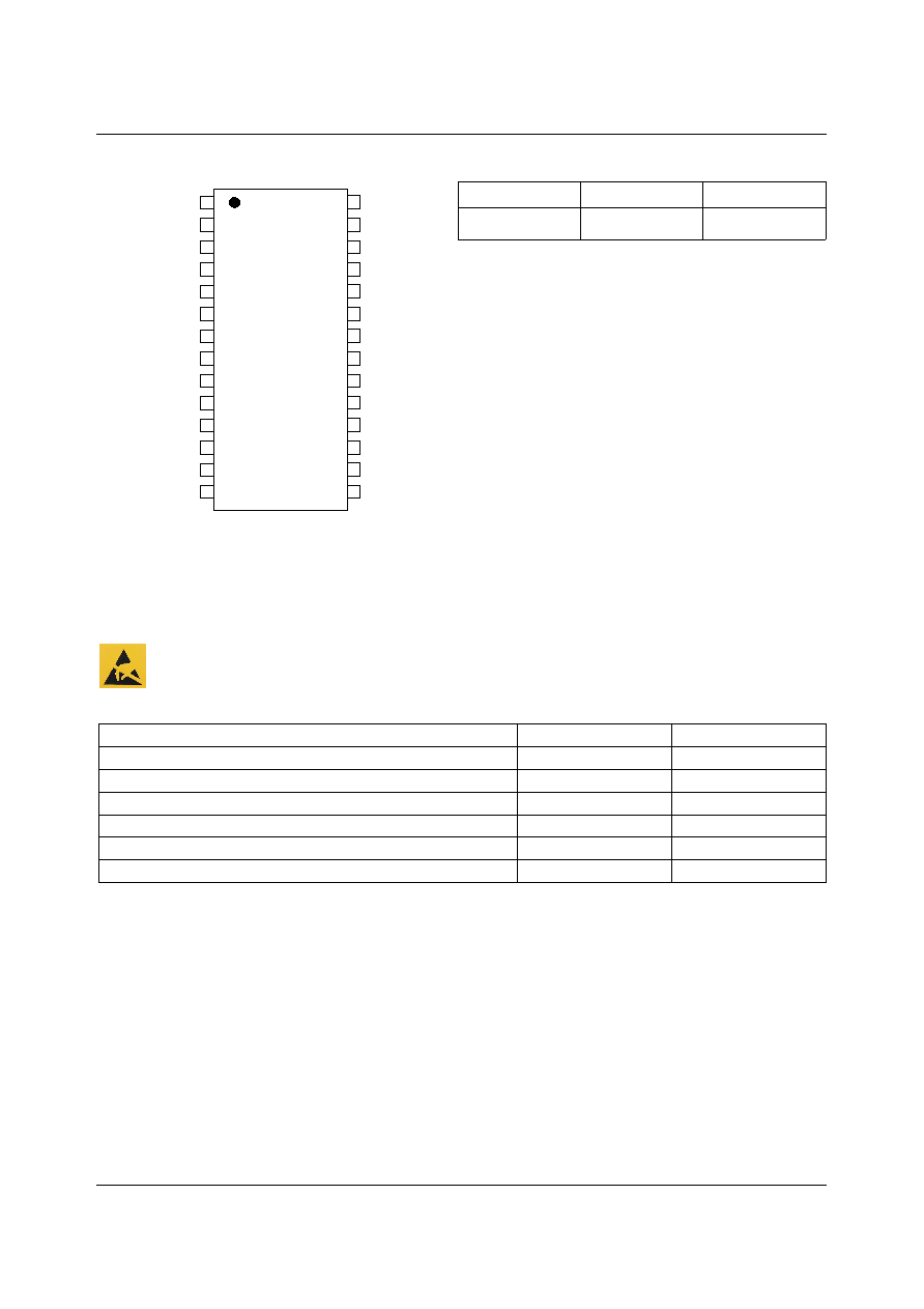
PIN CONFIGURATION
ORDERING INFORMATION
DEVICE
TEMP. RANGE
PACKAGE
WM8736EDS
-25
o
to 85
o
C
28-pin SSOP
16
15
14
20
19
18
17
5
6
7
1
2
3
4
13
12
11
8
9
10
BCKIN
MC/IWL
CAP
DVDD
SCKI
OUT1L
OUT0L
AGND2
GR1
OUT1R
GR0
OUT0R
AVDD2
DGND
GR2
DIN0
DIN1
LRCIN
RSTB
OUT2R
MUTE
MODE
AGND1
DIN2
21
22
23
24
25
26
27
28
ML/I2S
MD/DM
OUT2L
AVDD1
ABSOLUTE MAXIMUM RATINGS
Absolute Maximum Ratings are stress ratings only. Permanent damage to the device may be caused by continuously operating at
or beyond these limits. Device functional operating limits and guaranteed performance specifications are given under Electrical
Characteristics at the test conditions specified.
ESD Sensitive Device. This device is manufactured on a CMOS process. It is therefore generically susceptible
to damage from excessive static voltages. Proper ESD precautions must be taken during handling and storage
of this device.
CONDITION
MIN
MAX
Supply voltage
-0.3V
+7V
Reference input
VDD + 0.3V
Operating temperature range, T
A
-25
o
C
+85
o
C
Storage temperature
-65
o
C
+150
o
C
Package body temperature (soldering, 10 seconds)
+240
o
C
Package body temperature (soldering, 2 minutes)
+183
o
C

Production Data
WM8736
WOLFSON MICROELECTRONICS LTD
PD Rev 2.1 January 2001
3
RECOMMENDED OPERATING CONDITIONS
PARAMETER
SYMBOL
TEST CONDITIONS
MIN
TYP
MAX
UNIT
Digital supply range
DVDD
-10%
3.3 to 5
+10%
V
Analogue supply range
AVDD
-10%
3.3 to 5
+10%
V
Ground
AGND, DGND
0
V
Difference DGND to AGND
-0.3
0
+0.3
V
Analogue supply current
AVDD = 5V
50
mA
Digital supply current
DVDD = 5V
15
mA
Analogue supply current
AVDD = 3.3V
45
mA
Digital supply current
DVDD = 3.3V
15
mA
ELECTRICAL CHARACTERISTICS
Test Conditions
AVDD, DVDD = 5V, AGND, DGND = 0V, T
A
= +25
o
C, fs = 48kHz, SCKI = 256fs unless otherwise stated.
PARAMETER
SYMBOL
TEST CONDITIONS
MIN
TYP
MAX
UNIT
DAC Circuit Specifications
SNR (See Notes 1 and 2)
AVDD, DVDD = 5V
95
102
dB
AVDD, DVDD = 3.3V
100
dB
AVDD, DVDD = 5V
110
dB
SNR with automute on
AVDD, DVDD = 3.3V
108
dB
THD (full-scale)
(See Note 2)
0dB
-96
-85
dB
THD+N (Dynamic range)
(See Note 2)
-60dB
102
dB
Frequency response
0
20,000
Hz
Pass band ripple
0.125
dB
Transition band
20,000
Hz
Out of band rejection
-40
dB
Channel separation
90
dB
Gain mismatch
channel-to-channel
�1
%FSR
Digital Logic Levels
Input LOW level
V
IL
0.8
V
Input HIGH level
V
IH
2.0
V
Output LOW level
V
OL
I
OL
= 2mA
GND
+
0.3V
Output HIGH level
V
OH
I
OH
= 2mA
DVDD - 0.3V
Analogue Output Levels
Output level
Into 10kohm, full scale 0dB,
(5V supply)
1.1
V
RMS
Into 10kohm, full scale 0dB,
(3.3V supply)
0.72
V
RMS
To midrail or a.c. coupled
(5V supply)
1
kohms
Minimum resistance load
To midrail or a.c. coupled
(3.3V supply)
1
kohms
Maximum capacitance load
5V or 3.3V
100
pF
Output d.c. level
AVDD/2
V
Reference Levels
Potential divider resistance
AVDD to CAP and
CAP to AGND
90
kohms
Voltage at CAP
AVDD/2
POR
POR threshold
1.8
V

WM8736
Production Data
WOLFSON MICROELECTRONICS LTD
PD Rev 2.1 January 2001
4
BCKIN
DIN
LRCIN
t
BCH
t
BCL
t
BL
t
LB
t
BCY
t
DS
t
DH
Figure 1 Audio Data Input Timing
Test Conditions
AVDD, DVDD = 5V, AGND, DGND = 0V, T
A
= +25
o
C, fs = 48kHz, SCKI = 256fs unless otherwise stated.
PARAMETER
SYMBOL
TEST CONDITIONS
MIN
TYP
MAX
UNIT
Audio Data Input Timing Information
BCKIN pulse cycle time
t
BCY
100
ns
BCKIN pulse width high
t
BCH
50
ns
BCKIN pulse width low
t
BCL
50
ns
BCKIN rising edge
to LRCIN edge
t
BL
30
ns
LRCIN rising edge
to BCKIN rising edge
t
LB
30
ns
DIN setup time
t
DS
30
ns
DIN hold time
t
DH
30
ns
SCKI
t
SCKIL
t
SCKIH
Figure 2 System Clock Timing Requirements
Test Conditions
AVDD, DVDD = 5V, AGND, DGND = 0V, T
A
= +25
o
C, fs = 48kHz, SCKI = 256fs unless otherwise stated.
PARAMETER
SYMBOL
TEST CONDITIONS
MIN
TYP
MAX
UNIT
System Clock Timing Information
SCKI system clock pulse
width high
t
SCKIH
13
ns
SCKI system clock pulse
width low
t
SCKIL
13
ns

Production Data
WM8736
WOLFSON MICROELECTRONICS LTD
PD Rev 2.1 January 2001
5
ML/12S
MC/IWL
MD/DM
t
MLS
t
MLH
t
MLL
t
MCH
t
MCL
t
MCY
t
MDS
t
MDH
Figure 3 Program Register Input Timing
Test Conditions
AVDD, DVDD = 5V, AGND, DGND = 0V, T
A
= +25
o
C, fs = 48kHz, SCKI = 256fs unless otherwise stated.
PARAMETER
SYMBOL
TEST CONDITIONS
MIN
TYP
MAX
UNIT
Program Register Input Information
MC/IWL pulse cycle time
t
MCY
100
ns
MC/IWL pulse width low
t
MCL
50
ns
MD/DM pulse width high
t
MCH
50
ns
MD/DM set-up time
t
MDS
30
ns
MC/IWL hold time
t
MDH
30
ns
ML/I2S pulse width low
t
MLL
30
ns
ML/I2S set-up time
t
MLS
30
ns
ML/I2S hold time
t
MLH
30
ns
Notes:
1.
Ratio of output level with 1kHz full scale input, to the output level with all zeros into the digital input, measured "A"
weighted over a 20Hz to 20kHz bandwidth.
2.
All performance measurements done with 20kHz low pass filter. Failure to use such a filter will result in higher
THD+N and lower SNR and Dynamic Range readings than are found in the Electrical Characteristics. The low pass
filter removes out of band noise; although it is not audible it may affect dynamic specification values.