 | –≠–ª–µ–∫—Ç—Ä–æ–Ω–Ω—ã–π –∫–æ–º–ø–æ–Ω–µ–Ω—Ç: XE5686L | –°–∫–∞—á–∞—Ç—å:  PDF PDF  ZIP ZIP |

XECOM
(1)
XE5686L
XE5686L
12/00
Compact 56KBPS Data and Fax Modem
Description
Xecom's XE5686L combines high-speed data and
Group III send/receive fax in a compact component.
Xecom designed the XE5686L to be embedded by OEM
designers. Xecom also offers pin compatible 2400 BPS
14,400 BPS and 33,600 BPS alternatives to the
XE5686L for applications with other date rate
requirements.
The XE5686L is not a modem chip but a complete
modem including the telephone interface integrated into
a compact module. It provides user transferable FCC
Part 68 registration and can connect directly to the
telephone line through an RJ11 jack. The modem
connects to the host through a TTL level serial interface.
The XE5686L also includes MNP2-4, MNP10 and
V.42 error control and MNP5 and V.42bis data
compression to provide an error free connection with the
greatest possible data throughput rate.
Features
∑
Small Size; 1.385 " x 1.36" x 0.575"
∑
Modem control with "AT" commands
∑
Class 1 Fax commands
∑
Data transfer up to 56,000 bps
∑
Send and receive fax to 14,400 bps
∑
MNP and V.42 Error Control
∑
MNP10 Error Control for Cellular Links
∑
MNP5 Data Compression to 112,000 bps
∑
V.42bis Data Compression to 224,000 bps
∑
Low power, single +5V supply
Operating Power 800 mW (Typ.)
Sleep Mode 200 mW (Typ.)
∑
NVRAM for modem configuration storage
1 o
o 22
2 o
o 21
o 20
3 o
o 19
4 o
o 18
5 o
o 17
6 o
o 16
7 o
o 15
8 o
o 14
9 o
o 13
10 o
o 12
11 o
RING
TIP
N/C
N/C
SPK
N/C
N/C
N/C
N/C
TXD
RXD
RTS
RST
GND
VCC
N/C
/DCD
/CTS
/RI
/DSR
/DTR
/V-D
Modem
Controller
ROM
NVRAM
Analog
Front End
DAA
Tip
Ring
Spk
Gnd
(Top View)
VCC
RST
TXD
RXD
/DCD
/CTS
/DSR
/DTR
/RTS
/V-D
Block Diagram
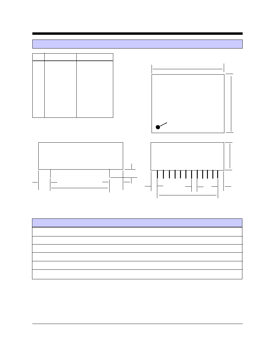
XE5686L Pin Configuration
XECOM
(2)
XE5686L
Dim
Min
Max
Min
Max
A
1.350
1.370
34.29
34.80
B
1.375
1.395
34.92
35.43
C
0.555
0.585
14.10
14.86
D
0.190
0.210
4.83
5.33
E
0.090
0.110
2.29
2.79
F
0.115
0.135
2.92
3.43
G
0.280
0.300
7.11
7.62
H
0.790
0.810
20.07
20.57
J
1.090
1.110
27.69
28.19
INCHES
METRIC(MM)
A
B
C
E
F
G
G
H
D
Denotes Pin 1
J
F
Pins = 0.025 inches Square
ABSOLUTE MAXIMUM RATINGS*
SUPPLY VOLTAGE - Vcc
+6.5 Volts
DC INPUT VOLTAGE
-0.6 Volts to +6.5 Volts
STORAGE TEMPERATURE RANGE
-25∞ C TO +85∞ C
LEAD TEMPERATURE (Soldering, 2 sec per wave)
260∞ C
OPERATING TEMPERATURE RANGE
0 TO 70∞ C
*Exceeding these values may result in permanent damage to the device.
XE5686L Mechanical Specifications
XECOM
(3)
XE5686L
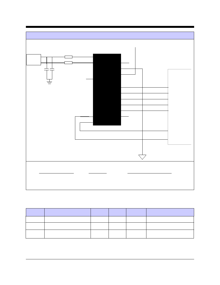
VCC
TXD
AMP
Host Serial
Interface
XE1486
3
4
RJ11
Ring
Tip
C1
C2
FB1
FB2
RXD
RST
Gnd
VCC
/DCD
/CTS
/RI
/DSR
/DTR
/V-D
Recommended Parts
Reference Designation
Description
Recommended Part Number
FB1, FB2
Ferrite Beads
TDK CB30-1812
C1, C2
Capacitors
Sprague 30GAT47, 470 pfd, 3000 Volts
Power Supply Characteristics
(TA = 0 - 70∞C, Vcc = 5v ±5%)
Vcc
Supply Voltage
5.0
5.25
Volts
Icc
Vcc Supply Current
160
180
mA
Active, On Line
40
60
mA
Sleep Mode
Symbol
Parameter
Typ
Max
Units
Comments
XE5686L
XE5686L Typical Connection Diagram

XECOM
(4)
XE5686L
XE5686L Pin Descriptions
PIN
NAME
DESCRIPTION
1
Ring
Ring provides half of the two-wire connection to the telephone network, RJ-11 Pin 4.
A 1500 volt barrier isolates Ring from all other circuits. This isolation must be pre-
served throughout the system. The battery voltage on Ring may be positive or negative
with respect to Tip.
2
Tip
Tip provides half of the two-wire connection to the telephone network, RJ-11 Pin 3. A
1500 volt barrier isolates Tip from all other circuits. This isolation must be preserved
throughout the system. The battery voltage on Tip may be positive or negative with re-
spect to Ring.
3, 4
Not Used
No Connection should be made to these pins.
5
SPK
SPK provides the audio output to a speaker. Speaker output is controlled by the ATL
and ATM commands. The input impedance to the speaker driver must be greater than
300 ohms.
6-9
N/C
No Connection
10
TXD
TXD provides serial data input from the host. A logic high represents a "Mark" and a
low represents a "Space".
11
RXD
RXD provides serial data output to the host. A logic high represents a "Mark" and a
low represents a "Space".
12
/V-D
The Voice-Data output can be used to drive an external relay for switching between the
modem and handset connected to the same telephone line.
13
/DTR
Data Terminal Ready is an active low input to the modem. The AT&D command sets
the function of DTR.
14
/DSR
Data Set Ready is an active low output from the modem. Its operation is determined by
the AT&S command.
15
/RI
Ring Indicator is an active low output which marks the presence of a ring on the line.
16
/CTS
The XE5686L uses Clear to Send for hardware flow control. With hardware flow con-
trol active the modem raises \CTS to signal the host that the modem's transmit data
buffer is nearly full. When the buffer empties, the modem reactivates CTS.
17
/DCD
Data Carrier Detect goes low to indicate receipt of a valid incoming carrier. The
AT&C1 command enables the carrier detect function.
18
N/C
No Connection
19
VCC
VCC provides the +5 volt power required by the modem.
20
GND
Ground provides the common reference for the XE5686L.
21
RST
This active high input causes a hardware reset in the XE5686L. The reset pulse must be held
high for at least 10 milliseconds to correctly reset the modem.
22
RTS
The modem uses Request to Send for hardware flow control. The modem stops sending data to
the host when the hosts raises /RTS. The modem resumes transferring data to the host when the
host activates /RTS

XECOM
(5)
XE5686L
Parameter
Min
Typ
Max
Unit
Comments
DTMF Level
-2.2
0
dBm
3 second average
Modem Transmit Level
-12
-10.5
-9.0
dBm
600 ohm line
Pulse Dialing Rate
10
pps
Pulse Dialing Make/Break
39/61
%
USA
Billing Delay Interval
2.0
sec.
Phone Line Impedance Match
600
ohms
Ring Detect Sensitivity
38
150
VRMS
Type B Ringer
Telephone Loop Current
20
100
milliamps
Off-hook
Input High Voltage (TXD, RTS, DTR)
2.0
Volts
Input Low Voltage (TXD, RTS, DTR)
0.8
Volts
Output High Voltage
2.4
Volts
RXD -100 microamps;
(DCD, DSR, CTS, RXD, RI, OH)
DCD, RI, OH - 1.6 milliamps
Output Low Voltage
0.4
Volts
RXD - 1.6 milliamps;
XE5686L Electrical Specifications
(TA = 0 - 70∞C, Vcc = 5v ±5%)