 | –≠–ª–µ–∫—Ç—Ä–æ–Ω–Ω—ã–π –∫–æ–º–ø–æ–Ω–µ–Ω—Ç: X9470V24I | –°–∫–∞—á–∞—Ç—å:  PDF PDF  ZIP ZIP |

Preliminary Information
REV 11.16 3/20/03
1 of 25
www.xicor.com
Preliminary Information
RF Power Amplifier (PA) Bias Controller
X9470
FEATURES
∑ Programmable Bias Controller IC for Class A and
AB LDMOS Power Amplifiers
∑ Adaptive System on Chip Solution
∑ Bias Current Calibration to better than ±4%
using Reference Trim DCP
∑ Automatic Bias Point Tracking and Calibration
-- I
DQ
Sensing and Tracking
--Programmable Instrumentation Amplifier to
Scale Wide Range of I
DQ
--Programmable Gate Bias Driver
--All Programmable settings are Nonvolatile
--All Settings Recalled at Power Up.
∑ 28V Maximum V
DD
∑ 2 Wire Interface for Programming Bias Setting
and Optimizing I
DQ
Set Point
∑ Bias Level Comparator
∑ Shutdown Control pin for PA Signal
∑ Slave address to allow for multiple devices
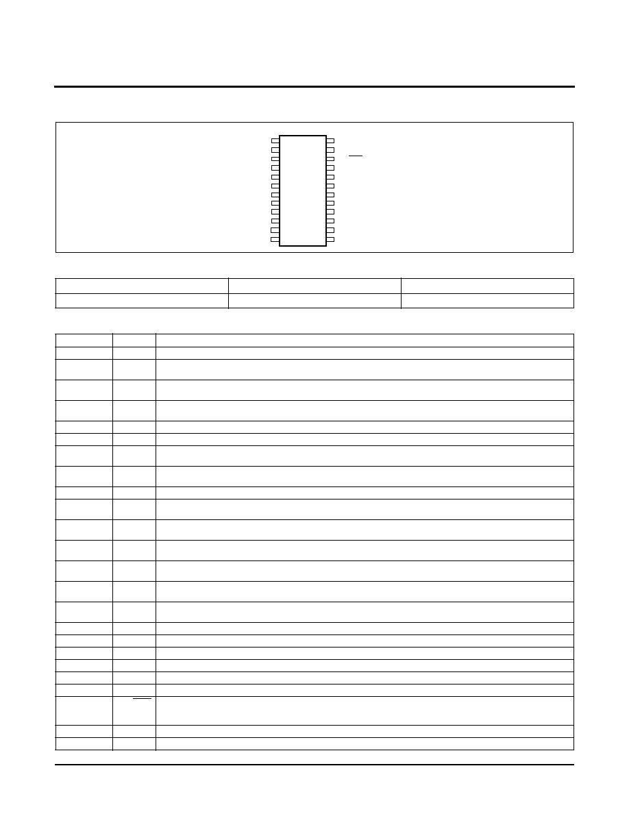
∑ 24-pin TSSOP Package
∑ Applications: Cellular Base Stations (GSM,
UMTS, CDMA, EDGE), TDD applications, Point-
to-multipoint, and other RF power transmission
systems
DESCRIPTION
The Xicor X9470 RF PA Bias Controller contains all of
the necessary analog components to sense the PA
drain current through an external sense resistor and
automatically control the gate bias voltage of an
LDMOS PA. The external sense resistor voltage is
amplified by an instrumentation amplifier and the out-
put of the amplifier along with an external reference
voltage is fed to the inputs of a comparator. The com-
parator output indicates which direction the LDMOS
gate bias voltage will move in the next calibration
cycle. System calibration is accomplished by enabling
the X9470 and providing a clock to the SCL pin. The
LDMOS drain current can be maintained constant over
temperature and aging changes by periodic calibra-
tion. The VOUT pin can be used to monitor the aver-
age power by tracking the drain current. Up to eight
X9470 or additional Xicor Digital Potentiometers can
be controlled via a two-wire serial bus.
TYPICAL APPLICATION
A0
A2
VCC
VSS
V+
AGND
Comparator
choke
RF PA in
R
SENSE
V
DD
V
REF
V
SENSE+
V
BIAS
INC/DEC
Instrumentation
Amplifier
V
CS
V
OUT
V
SENSE≠
R
REF
RW
REF
RL
REF
SHDN
+
≠
EEPROM
SCL
SDA
A1
Vbias
control
VREF
control
I2C
interface
Control &
Status Registers
RF
out
RH
REF
R
BIAS
VP
RH
BIAS
RL
BIAS
RW
BIAS
FILTER
V
BIAS (Unbuffered)
RF Impedance
Matching
C
BULK
Class A Example
Preliminary Information
2 of 25
REV 11.16 3/20/03
www.xicor.com
Preliminary Information
X9470
PIN CONFIGURATION
ORDERING INFORMATION
PIN DESCRIPTIONS
Part Number
Temperature Range
Package
X9470V24I
-40∞C TO 85∞C
24-Lead TSSOP
TSSOP pin
Symbol
Brief Description
1
V
SENSE+
Positive sense voltage input terminal
2
RH
REF
Upper Terminal of Potentiometer, called the R
REF
potentiometer. The voltage applied to this pin will determine the
upper voltage limit of the adjustment for the Up/Down threshold of the comparator.
3
RL
REF
Lower Terminal of Potentiometer, called the R
REF
potentiometer. The voltage applied to this pin will determine the
lower voltage limit of the adjustment for the Up/Down threshold of the comparator.
4
RW
REF
Wiper Terminal of Potentiometer, called the R
REF
potentiometer. The voltage on this pin will be the threshold for
the Up/Down comparator. Also referred to as the V
REF
of the comparator.
5
AGND
Analog ground to allow single point grounding external to the package to minimize digital noise.
6
VSS
System (Digital) Ground Reference
7
CS
Chip Select. This input enables bias calibration adjustments to the R
BIAS
potentiometer. CMOS input with internal
pull-down.
8
SCL
Dual function. Function 1: The increment control input. Increments or decrements the R
BIAS
potentiometer.
Function 2: Serial Data Clock Input. Requires external pull-up.
9
SDA
Serial Data Input. Bi-directional 2-wire interface. Requires external pull-up.
10
RH
BIAS
Upper Terminal of Potentiometer, called the R
BIAS
potentiometer. The voltage applied to this pin will determine the
upper limit of the bias voltage to the PA (or V
BIAS
pin).
11
RW
BIAS
Wiper Terminal of Potentiometer, called the R
BIAS
potentiometer. This voltage is the equivalent to the unbuffered
voltage that will appear at the V
BIAS
pin.
12
RL
BIAS
Lower Terminal of Potentiometer, called the R
BIAS
potentiometer. The voltage applied to this pin will determine the
lower limit of the bias voltage to the PA (or V
BIAS
pin).
13
A0
External address pin which allows for a hardware slave address selection of this device.
This pin has an internal pull-down.
14
A1
External address pin which allows for a hardware slave address selection of this device.
This pin has an internal pull-down.
15
A2
External address pin which allows for a hardware slave address selection of this device.
This pin has an internal pull-down.
16
VSS
System (Digital) Ground Reference
17
V
BIAS
This is the bias output voltage pin and is used to drive the filter network to the PA gate.
18
V
CC
System (Digital) Supply Voltage
19
V
CC
System (Digital) Supply Voltage
20
V +
Positive voltage supply for the instrumentation amplifier and other analog circuits.
21
V
OUT
Instrumentation Amplifier output that is 20x or 50x the voltage across the Rsense pins.
22
INC/DEC
Status output that indicates the state of the comparator. When this pin is HIGH, the RBIAS potentiometer will in-
crement; when the pin is LOW, the RBIAS potentiometer will decrement. This pin is open drain and requires ex-
ternal resistor pull-up.
23
SHDN
Shutdown the output op amp. When SHDN is active (HIGH), the V
BIAS
pin is pulled LOW.
24
V
SENSE-
Negative sense voltage Input terminal
V
OUT
RW
REF
V+
TSSOP
1
2
3
4
5
6
7
14
20
19
18
17
16
15
X9470
V
sense+
V
sense-
RH
REF
RL
REF
VSS
AGND
SHDN
INC/DEC
V
CC
A2
RH
BIAS
V
CC
SDA
SCL
V
BIAS
VSS
CS
8
9
10
13
RL
BIAS
RW
BIAS
11
12
A0
A1
24
23
22
21
Preliminary Information
3 of 25
REV 11.16 3/20/03
www.xicor.com
Preliminary Information
X9470
ABSOLUTE MAXIMUM RATINGS*
Voltage on V+ (referenced to AGND)....................... 7V
Voltage on VCC (reference to VSS)......................... 7V
Voltage on all RH, RW, RL pins
(reference to AGND): ........................................... 7V
Voltage on Vsense+ or
Vsense- (reference to AGRND).......................... 30V
Voltage on SDA, CS, SCL, SHDN
(reference to AGND) ............... -0.3V to (Vcc + 0.3V)
Current into Output Pin:
..........................................±
5mA
Continuous Power Dissipation:........................ 500mW
Operating Temperature range: ...............-40
∞
C to +85
∞
C
Junction Temperature:........................................... 150
∞
C
Storage Temperature......................... -65
∞
C to +150
∞
C
Lead Temperature (Soldering, 10 seconds): ..... 300
∞
C
*COMMENT
Stresses above those listed under "Absolute Maximum
Ratings" may cause permanent damage to the device.
This is a stress rating only and the functional operation
of the device at these or any other conditions above
those listed in the operational sections of this specifi-
cation is not implied. Exposure to absolute maximum
rating conditions for extended periods may affect
device reliability.
ELECTRICAL CHARACTERISTICS
INSTRUMENTATION AMPLIFIER
Recommended Operating Conditions: (Vcc, V+ = 4.75 to 5.25V; Vsense+, Vsense- = 26V; T
A
= -40∞C to +85∞C,
unless otherwise noted.)
Symbol
Parameter
Limits
Test Conditions/Notes
Min. Typ. Max. Units
V
IN
(10)
Common Mode Input Voltage on
V
SENSE+
and V
SENSE-
pins
20
28
V
Gain 1
Gain from V
SENSE
to V
OUT
(2)
20
V/V
Measured with Status
Register bit SR0=0
Gain 2
Gain from V
SENSE
to V
OUT
(2)
50
V/V
Measured with Status
Register bit SR0=1
V
RANGE1
Differential voltage sense range be-
tween V
SENSE+
and V
SENSE-
for gain 1
60
90
mV
Gain = 20
V
RANGE2
Differential voltage sense range be-
tween V
SENSE+
and V
SENSE-
for gain 2
40
60
mV
Gain = 50
V
OS
Input Offset Voltage
0.5
mV
V
SENSE
= 40mV to 90mV
T
A
= 25∞C
Av1
Gain 1 Error
Gain = 20 (4)
1.5
%
V
SENSE
= 60mV to 90mV
T
A
= 25 to 85∞C, Gain = 20
Av2
Gain 2 Error
Gain = 50 (4)
1.5
%
V
SENSE
= 40mV to 60mV
T
A
= 25 to 85∞C, Gain = 50
Avt1
Total Error, Gain 1
Gain = 20 (5)
-6
1.5
6
%
V
SENSE
= 60mV to 90mV
T
A
= 85∞C, Gain = 20
10
%
V
SENSE
= 60mV to 90mV
T
A
= 25 to 85∞C, Gain = 20
Avt2
Total Error, Gain 2
Gain = 50 (5)
-6
1.5
6
%
V
SENSE
= 40mV to 60mV
T
A
= 85∞C, Gain = 50
10
%
V
SENSE
= 40mV to 60mV
T
A
= 25 to 85∞C, Gain = 50
At
Long Term Drift
2
%
Avt1 or Avt2
Preliminary Information
4 of 25
REV 11.16 3/20/03
www.xicor.com
Preliminary Information
X9470
COMPARATOR
Recommended Operating Conditions: (Vcc, V+ = 4.75 to 5.25V; Vsense+, Vsense- = 26V; T
A
= -40∞C to +85∞C, unless
otherwise noted.)
SR
(10)
Slew Rate of Instrumentation Amp
0.2
V/µS
V
SENSE
= 20mV step,
Cout = 10pF Measured at
V
OUT
(1,3)
T
settle
(10)
Setting time of Instrumentation Amp
5.0
µS
V
SENSE
= 20mV step, Cout =
10pF, settling to 1% of final value
Measured at V
OUT
(1,3)
CMRR
Common Mode Rejection Ratio
40
dB
For both Gain 1 and Gain 2
PSRR
Power Supply Rejection Ratio
55
dB
For both Gain 1 and Gain 2
V
OUT
Range
V
OUT
Voltage Swing
0.3
1.8
V
Gain = 20
0.3
3.0
V
Gain = 50
V
OUT
Noise
(10)
V
OUT
Voltage Noise, rms
3
mV
Gain = 20
I
VSENSE
(10)
V
SENSE+
, V
SENSE-
Input Bias
Current
250
µA
T
A
= 25∞C
C
VSENSE
(10)
V
SENSE+
, V
SENSE-
Input
Capacitance
10
pF
Each Input
Symbol
Parameter
Limits
Test Conditions/Notes
Min.
Typ.
Max. Units
VOL
Output Voltage Low on the
INC/DEC
pin
0.4
V
IOL = 1mA
Io
(10)
Output sink Current
3
mA
INC/DEC
pin, open drain
Vos
(10)
Input Hysteresis
20
mV
Vcc = 5 V
Tpd
(10)
Response Time for propagation delay
2
µS
INC/DEC
pin with 2K
pull up
VREF DCP CIRCUIT BLOCK
Recommended Operating Conditions: (Vcc, V+ = 4.75 to 5.25V; Vsense+, Vsense- = 26V; T
A
= -40∞C to +85∞C,
unless otherwise noted.)
Symbol
Parameter
Limits
Test Conditions/Notes
Min.
Typ.
Max.
Units
R
TOTAL
End to End Resistance
8
10
12
K
Number Taps or Positions
64
V
RH
RH
REF
Terminal Voltage
AGND
V
+
V
AGND
= 0V
V
RL
RL
REF
Terminal Voltage
AGND
V
+
V
AGND
= 0V
V
RW
RW
REF
Terminal Voltage
AGND
V
+
V
AGND
= 0V
Power Rating
(10)
2.5
mW
R
TOTAL
=10 K
ELECTRICAL CHARACTERISTICS
INSTRUMENTATION AMPLIFIER (CONTINUED)
Recommended Operating Conditions: (Vcc, V+ = 4.75 to 5.25V; Vsense+, Vsense- = 26V; T
A
= -40∞C to +85∞C,
unless otherwise noted.)
Symbol
Parameter
Limits
Test Conditions/Notes
Min. Typ. Max. Units

Preliminary Information
5 of 25
REV 11.16 3/20/03
www.xicor.com
Preliminary Information
X9470
BIAS ADJUSTMENT DCP CIRCUIT BLOCK
Recommended Operating Conditions: (Vcc, V+ = 4.75 to 5.25V; Vsense+, Vsense- = 26V; T
A
= -40∞C to +85∞C, unless
otherwise noted.)
Resolution
(10)
1.6
%
Absolute Linearity
(6)
-0.2
+0.2
MI
(8)
Relative Linearity
(7)
-0.2
+0.2
MI
(8)
R
TOTAL
Temperature Coefficient
(10)
±300
ppm/∞C
Ratiometric Temperature Coefficient
(10)
-20
+20
ppm/∞C
C
IN
(10)
Potentiometer Capacitances on RH
REF
and RL
REF
10
pF
Symbol
Parameter
Limits
Test Conditions/Notes
Min.
Typ.
Max.
Units
R
TOTAL
End to End Resistance Variation
8
10
12
K
with ±20% variation
Number Taps or Positions
256
V
RH
Voltage at the RH
BIAS
Terminal Voltage
AGND
V
+
V
AGND
= 0V
V
RL
Voltage at the RL
BIAS
Terminal Voltage
AGND
V
+
V
AGND
= 0V
V
RW
Voltage at the RW
BIAS
Terminal Voltage
AGND
V
+
V
AGND
= 0V
Power Rating
(10)
2.5
mW
R
TOTAL
=10 K
Resolution
(10)
0.4
%
Absolute Linearity
(6)
-1.0
+1.0
MI
(8)
Relative Linearity
(7)
-1.0
+1.0
MI
(8)
R
TOTAL
Temperature Coefficient
(10)
±300
ppm/∞C
Ratiometric Temperature Coefficient
(10)
-50
50
ppm/∞C
C
IN
(10)
Potentiometer Capacitances on RH
BIAS
and RL
BIAS
10
pF
VBIAS OUTPUT VOLTAGE FOLLOWER
Recommended Operating Conditions: (Vcc, V+ = 4.75 to 5.25V; Vsense+, Vsense- = 26V; T
A
= -40∞C to +85∞C,
unless otherwise noted.)
Symbol
Parameter
Limits
Test Conditions/Notes
Min.
Typ.
Max.
Units
V
OS
Input Offset Voltage
10
mV
V
OSDRIFT
(10)
Offset Voltage Temperature
Coefficient
10
µV/∞C
T
A
= -40 to +85∞C
SR
Output Slew Rate on
V
BIAS
0.5
V/
µS
R
L
= 10k
, 1nF, V
BIAS
=
20mV
V
BIAS
Voltage Output Swing
1.5
V
CC
≠ 0.5
V
I
OUT
= ±10mA
VREF DCP CIRCUIT BLOCK
Recommended Operating Conditions: (Vcc, V+ = 4.75 to 5.25V; Vsense+, Vsense- = 26V; T
A
= -40∞C to +85∞C,
unless otherwise noted.)
Symbol
Parameter
Limits
Test Conditions/Notes
Min.
Typ.
Max.
Units
Preliminary Information
6 of 25
REV 11.16 3/20/03
www.xicor.com
Preliminary Information
X9470
D.C. OPERATING CHARACTERISTICS
Recommended Operating Conditions: (Vcc, V+ = 4.75 to 5.25V; Vsense+, Vsense- = 26V; T
A
= -40∞C to +85∞C, unless
otherwise noted.)
Notes: (1) V
OUT
is a high impedance output intended for light loads only.
(2) Gain at V
OUT
is set to 20 by default.
(3) Value given is for V
OUT
. The V
BIAS
output will depend on the V
BIAS
potentiometer which is initially loaded with a zero value, then
followed by the loading of the final value from E
2
memory.
(4) Gain Error excludes the contribution of the input offset voltage error
(5) Total Error includes the contributions of gain error and input offset voltage error.
(6) Absolute Linearity is utilized to determine actual wiper voltage versus expected voltage = (V
w(n)
(actual) ≠ V
w(n)
(expected))
(7) Relative Linearity is a measure of the error in step size between taps = V
W(n+1)
≠ [V
w(n)
+ Ml]
(8) 1 Ml = Minimum Increment = R
TOT
/63 or R
TOT
/255.
(9) Typical values are for T
A
= 25∞C and nominal supply voltage, VCC = 5V
(10) This parameter is not 100% tested.
T
S
(10)
Settling Time
2
µs
Final value ±1%, R
L
= 10k
,
1nF,
V
BIAS
= 20mV
t
SHDN
Time for
SHDN
pin (delay) valid
0.1
1.0
µs
PSRR
Power Supply Rejection Ratio
45
55
dB
VCC supply V
CC
= 4.75 to
5.25V
Input Voltage Range
1.5
V
CC
≠ 0.5
V
C
L
(10)
Load Capacitance
1
nF
C
IN
(10)
Capacitances on Shutdown Pin
10
pF
R
OUT
(10)
Output Impedance
3
at 5MHz, 1nF load
Symbol
Parameter
Limits
Units
Test Conditions
Min.
Typ.
Max.
I
CC1
(9)
V+ Active Current
1
3
mA
CS
= V
CC
≠ 0.3V, and SCL
@ max. t
CYC, SDA =
V
CC
≠
0.3V, SHDN inactive
I
CC2
(9)(10)
V
CC
Active Current
5
25
mA
I
SB
(9)
Standby Supply Current
(V
CC
, V+)
1.5
mA
CS
= V
IL
, and SCL inactive
(no clock)
, SDA =
V
IL
, SHDN
active
I
LI
CS, SDA, SCL, SHDN RH, RL, RW,
INC/DEC VOUT, Input Leakage
-10
10
µA
V
IN
= VSS to V
CC
V
IH
(10)
CS, SDA, SCL, SHDN, A0, A1, A2
HIGH Voltage
V
CC
x 0.7
V
CC
+ 0.5
V
V
IL
(10)
CS, SDA, SCL, SHDN, A0, A1, A2
LOW Voltage
≠0.5
V
CC
x 0.3
V
C
IN
(10)
CS, SDA, SCL, SHDN, A0, A1, A2
Capacitance
10
pF
V
CC
= 5V, V
IN
= VSS,
T
A
= 25∞C, f = 1MHz
VBIAS OUTPUT VOLTAGE FOLLOWER
Recommended Operating Conditions: (Vcc, V+ = 4.75 to 5.25V; Vsense+, Vsense- = 26V; T
A
= -40∞C to +85∞C,
unless otherwise noted.)
Symbol
Parameter
Limits
Test Conditions/Notes
Min.
Typ.
Max.
Units

Preliminary Information
7 of 25
REV 11.16 3/20/03
www.xicor.com
Preliminary Information
X9470
BIAS ADJUSTMENT CIRCUIT BLOCK
A.C. OPERATING CHARACTERISTICS
Recommended Operating Conditions: (Vcc, V+ = 4.75 to 5.25V; Vsense+, Vsense- = 26V; T
A
= -40∞C to +85∞C, unless
otherwise noted.)
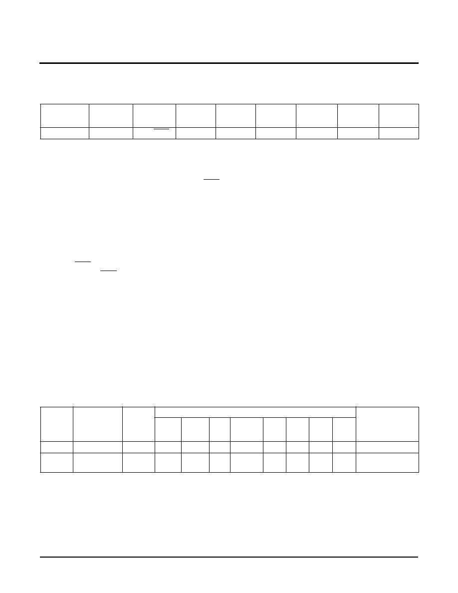
A.C. TIMING
Note:
(11) MI in the A.C. timing diagram refers to the minimum incremental change in the V
BIAS
output due to a change in the wiper position.
Symbol
Parameter
Limits
Units
Min.
Typ.
(9)
Max.
t
Cl
CS
to SCL Setup
100
ns
t
lD
Vsense Change to
INC/DEC
Change
5
µs
t
lL
SCL LOW Period
1.5
µs
t
lH
SCL HIGH Period
1.5
µs
t
lC
(10)
SCL Inactive to
CS
Inactive
100
ns
t
IW
(10)(11)
SCL to
V
BIAS
Change
3
µs
t
CYC
SCL Cycle Time
3
µs
t
R,
t
F
(10)
SCL Input Rise and Fall Time
500
ns
CS
SCL
INC/DEC
V
BIAS
t
CI
t
IL
t
IH
t
CYC
t
ID
t
IW
t
IC
t
F
t
R
10%
90%
90%
(Vsense+ ≠
Vsense-)

Preliminary Information
8 of 25
REV 11.16 3/20/03
www.xicor.com
Preliminary Information
X9470
AC SPECIFICATIONS
Note:
(12) Cb = total capacitance of one bus line in pF.
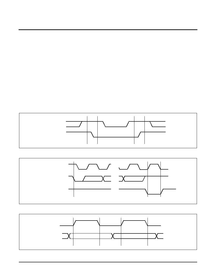
TIMING DIAGRAMS
Bus Timing
Symbol Parameter
Min.
Max.
Unit
f
SCL
SCL Clock Frequency
0
400
kHz
t
IN
(10)
Pulse width Suppression Time at inputs
50
ns
t
AA
(10)
SCL LOW to SDA Data Out Valid
0.1
0.9
µs
t
BUF
(10)
Time the bus must be free before a new transmission can start
1.3
µs
t
LOW
Clock LOW Time
1.3
µs
t
HIGH
Clock HIGH Time
0.6
µs
t
SU:STA
Start Condition Setup Time
0.6
µs
t
HD:STA
Start Condition Hold Time
0.6
µs
t
SU:DAT
Data In Setup Time
200
ns
t
HD:DAT
Data In Hold Time
200
ns
t
SU:STO
Stop Condition Setup Time
0.6
µs
t
DH
(10)
Data Output Hold Time
50
ns
t
R
(10)
SDA and SCL Rise Time
20 +.1Cb
(12)
300
ns
t
F
(10)
SDA and SCL Fall Time
20 +.1Cb
(12)
300
ns
Cb
(10)
Capacitive load for each bus line
400
pF
t
SU:STO
t
DH
t
HIGH
t
SU:ST
t
HD:STA
t
HD:DAT
t
SU:DAT
SCL
SDA IN
SDA OUT
t
F
t
LOW
t
BUF
t
AA
t
R

Preliminary Information
9 of 25
REV 11.16 3/20/03
www.xicor.com
Preliminary Information
X9470
Write Cycle Timing
Power Up Timing
Note:
Delays are measured from the time V
CC
is stable until the specified operation can be initiated. These parameters are not 100% tested.
Proper recall of stored wiper setting requires a V
CC
power-up ramp that is monotonic and with noise or glitches < 100mV. It is important
to correctly sequence voltages in an LDMOS amplifier circuit. For the X9470 typical application, the V
CC
, then V+ pins should be pow-
ered before the V
DD
of the LDMOS to prevent LDMOS damage. Under no circumstances should the V
DD
be applied to the LDMOS
device before V
CC
and V+ are applied to the X9470.
DCP Default Power-up Tap Positions (shipped from factory)
Nonvolatile Write Cycle Timing
Note:
t
WC
is the time from a valid stop condition at the end of a write sequence to the end of the self-timed internal nonvolatile write cycle. It is
the minimum cycle time to be allowed for any nonvolatile write by the user, unless Acknowledge Polling is used.
Symbol Parameter
Min.
Max.
Unit
t
r
V
CC
(10)
V
CC
Power-up rate
0.2
50
V/ms
VREF DCP
0
Bias Adjust DCP
0
Symbol Parameter
Min.
Typ.
(1)
Max.
Unit
t
WC
(10)
Write Cycle Time
5
10
ms
SCL
SDA
t
WC
8th Bit of Last Byte
ACK
Stop
Condition
Start
Condition

Preliminary Information
Preliminary Information
X9470
10 of 25
REV 11.16 3/20/03
www.xicor.com
DETAILED PIN DESCRIPTIONS
Supply Pins
Digital Supplies VCC, VSS
The positive power supply and ground for the DCP dig-
ital control sections. VSS is normally tied to digital
ground. The X9470 is provided with separate digital
and analog power supply pins to better isolate digital
noise from the analog section.
Analog Supplies V+, AGND
The positive analog supply and ground for the Instru-
mentation Amplifier (IA). The analog supply ground is
kept separate to allow an external single point connec-
tion. V+ can be a separate supply voltage from VCC, or
VCC can be filtered before connection to V+.
Bias Adjustment Circuit Block Pins
RH
BIAS
, RL
BIAS
, and RW
BIAS
for
VBIAS Adjust-
ments.
These pins are the connections to a Xicor Digitally
Controlled Potentiometer (XDCP
TM
) or R
BIAS
potenti-
ometer. RH
BIAS
is connected to the most positive refer-
ence, and the RL
BIAS
is connected to the least positive
reference voltage. The potentiometer has a resolution
of 256-taps and typical R
TOTAL
of 10kohm. So for
example, to provide 4mV resolution, the voltage differ-
ence applied to the RH
BIAS
and RL
BIAS
pins must be
1.024V. The RW
BIAS
value can be stored in non-vola-
tile memory and recalled upon power up.
Serial Clock (SCL).
This is a dual function input pin. The state of the CS pin
determines the functionality.
Function 1:
SCL
is a negative edge-triggered control
pin of the R
BIAS
potentiometer. Toggling
SCL
will
either increment or decrement the wiper in the
direction indicated by the logic level on the INC/DEC
pin. CS must be high for this function.
Function 2: SCL is the serial bus clock for serial bus
interface. CS must be low for this function.
Chip Select (CS). Calibration Enable.
The CS input is the enable bias adjustments. When the
CS is HIGH (enabled) and a SCL pulse is present, the
wiper position on the R
BIAS
potentiometer will auto-
matically update with either an increment or decrement
of one tap position according to INC/DEC signal from
the comparator.
When CS is LOW (disabled), the wiper counter of the
XDCP will hold the last wiper position until CS is
enabled again and the wiper position is updated.
INC/DEC Monitor Pin
The Up or Down Monitor pin (INC/DEC) indicates the
state of the comparator. This signal indicates that the
Instrumentation Amplifier output voltage is higher or
lower than the voltage level set by the RW
REF
pin. The
output is used to indicate the direction that the gate
bias voltage needs to move to reach the target bias
voltage.
Sense and Scale Block Pins
V
SENSE+
and V
SENSE-
These are the input pins to the IA circuit. These pins
are used to determine the change in voltage across the
the external drain sense resistor of an RF power ampli-
fier.
RH
REF
, RL
REF
, and RW
REF
. PA Bias Set Point.
The PA Bias reference voltage is controlled by a 64-tap
(10k ohm typical R
TOTAL
) potentiometer, called the
R
REF
potentiometer. The voltages applied to RH
REF
and RL
REF
will determine the range of adjustment of
the reference voltage level (VREF) for the Comparator.
The resolution of the comparator reference is the differ-
ence of the voltages applied to RH
REF
and RL
REF
divided by 63. The position of the wiper (RW
REF
) is
controlled via serial bus. The RW
REF
value can be
stored in non-volatile memory and recalled upon power
up.
RW
REF
is also an input signal used as a scaling volt-
age (VREF) to set the appropriate I
DQ
of an RF power
amplifier. V
REF
can be derived from an external voltage
divider or from a baseband processor or similar micro-
controller. V
REF
can be set permanently or changed
dynamically using the potentiometer for various PA
operating points.

Preliminary Information
11 of 25
REV 11.16 3/20/03
www.xicor.com
Preliminary Information
X9470
V
OUT
This pin is the output of the IA, which reflects a 20x or
50x gain of the input signal (voltage across the Vsense
pins). It can be used to indicate the magnitude of the
drain current envelope when RF is present.
Output Block Pins
V
BIAS
The V
BIAS
is the gate bias voltage output. It is buffered
with a unity gain amplifier and is capable of driving 1nF
(typical) capacitive loads.
This pin is intended to be connected through an RF fil-
ter to the gate of an LDMOS power transistor. The volt-
age of V
BIAS
is determined by the XDCP's value of the
R
BIAS
resistor.
Other Pins
SHDN
SHDN is an input pin that is used to shutdown the
V
BIAS
output voltage follower. When the SHDN pin is
HIGH, the V
BIAS
pin is pulled to VSS. When the device
is shutdown, the current R
BIAS
wiper position will be
maintained in the wiper counter register. When shut-
down is disabled, the wiper returns to the same wiper
position before shutdown was invoked. Note that when
the device is taken out of shutdown mode (SHDN goes
from HIGH to LOW), the CS input must be cycled once
to enable calibration.
SDA
Serial bus data input/output. Bi-directional. External
pullup is required.
A0, A1, A2
Serial bus slave address pins. These pins are used to
defined a hardware slave address. This will allow up to
8 of the X9470's to be shared on one two-wire bus.
These are useful if several X9470's are used to control
the bias voltages of several LDMOS Power Transistors
in a single application. Default hardware slave address
is "000" if left unconnected due to internal pull-down
resistor.
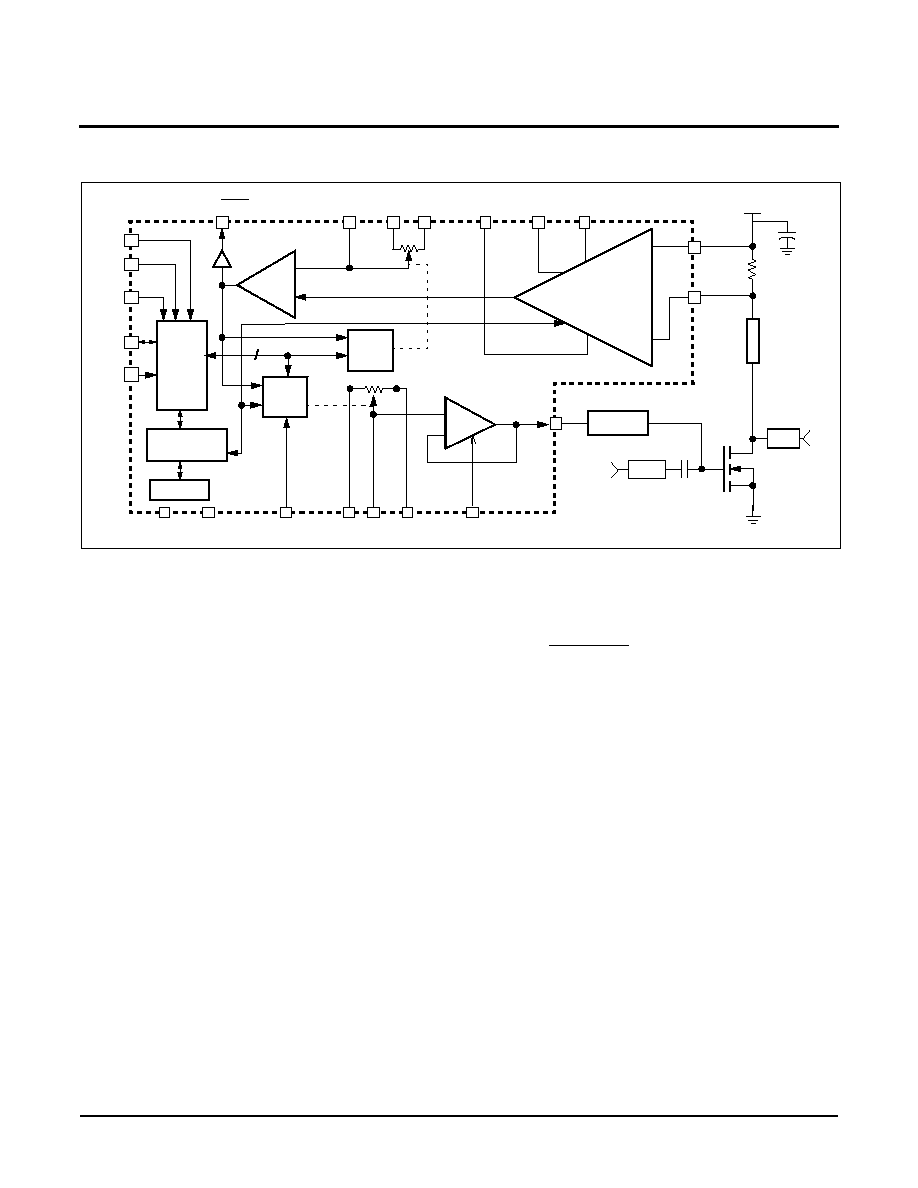
TYPICAL APPLICATION
The X9470 can be used along with a microprocessor
and transmit control chips to control and coordinate
FET biasing (see Figure 1). The CS, SCL, and SDA
signals are required to control the X9470 Bias Adjust-
ment Circuit Block. An internal R
WREF
voltage is pro-
vided via a programmable voltage divider between the
RH
REF
and RL
REF
pins and is used to set the voltage
reference of the comparator. The shutdown (SHDN)
and bias voltage indicators (INC/DEC) are additional
functions that offer FET control, monitoring, and pro-
tection.
Typically, the closed loop setup of the X9470 allows for
final calibration of a power amplifier at production test.
The CS and SCL pins are used to perform this calibra-
tion function. Once in a base station, the amplifier can
then be re-calibrated any time that there is no RF sig-
nal present. The bias setting block can also be used
open loop to adjust gate bias or can be shutdown
using the SHDN pin. The sense and scale block can be
used for amplifier power monitoring diagnostics as
well.
The range of the drain bias current operating point of
the LDMOS FET is set by an external reference across
the reference potentiometer. The wiper of the potenti-
ometer sets the trip point for comparison with V
P
, the
amplified voltage across R
SENSE
, the drain resistor.
The output of the comparator causes the R
BIAS
poten-
tiometer to increment or decrement automatically on
the next SCL clock cycle. This R
BIAS
potentiometer is
configured as a voltage divider with a buffered wiper
output which drives the gate voltage of an external
LDMOS FET.
Once the optimum bias point is reached, the R
BIAS
value is latched into a wiper counter register. Again,
the V
BIAS
gate voltage can be updated continuously or
periodically depending on the system requirements.
Both terminals of the R
BIAS
potentiometer are access-
ible and can be driven by external reference voltages
to achieve a desired I
DQ
vs. gate voltage resolution, as
well as supporting temperature compensation circuitry.
In summary, the X9470 provides full flexibility on set-
ting the operating bias point and range of an external
RF power amplifier for GSM, EDGE, UMTS, CDMA or
other similar applications.
Preliminary Information
Preliminary Information
X9470
12 of 25
REV 11.16 3/20/03
www.xicor.com
Figure 1. Typical Application
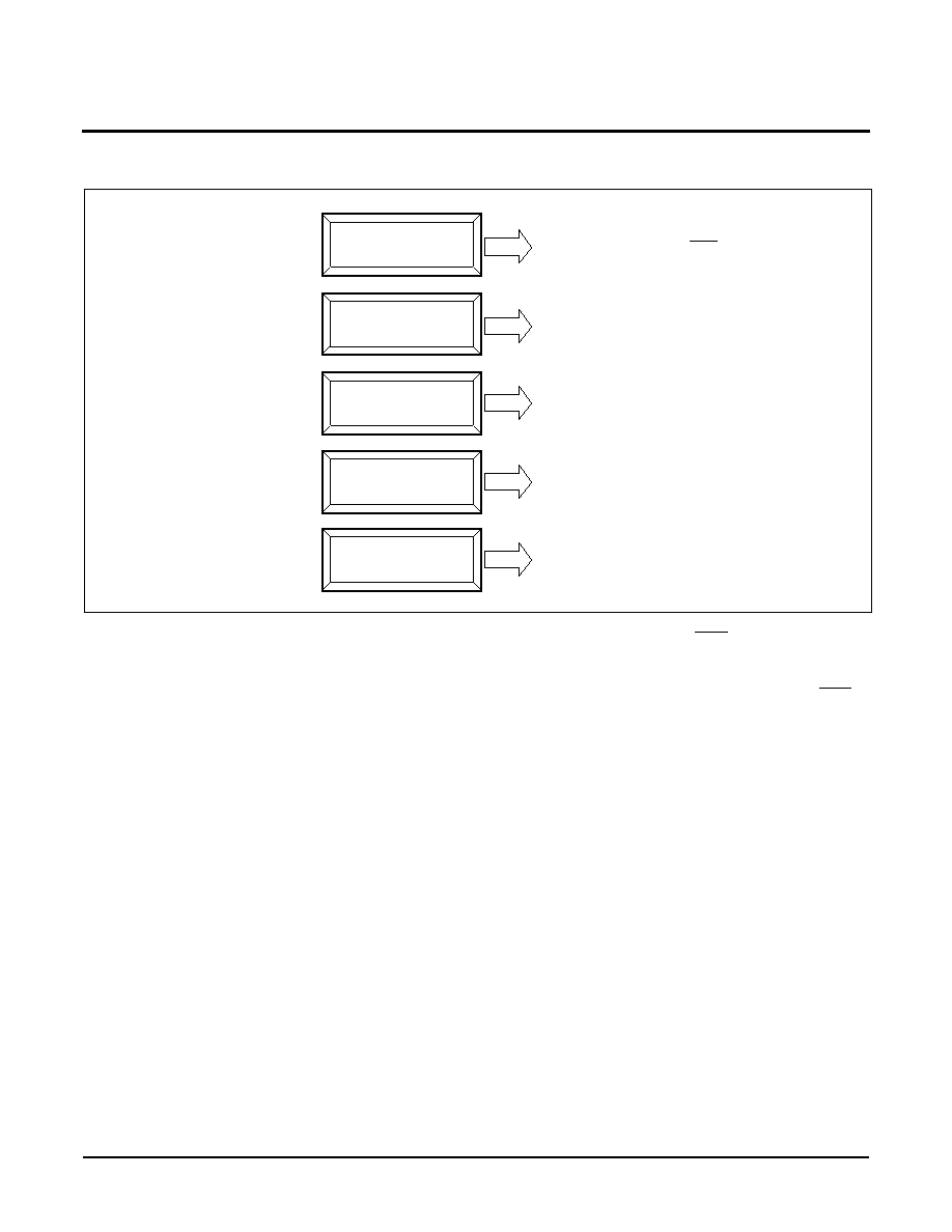
X9470 FUNCTIONAL DESCRIPTION
This section provides detail description of the following:
≠ Sense and Scale Block Description
≠ Bias Adjustment Control Block Description
≠ Output Block Description
≠ Bias Adjustment and Storage Description
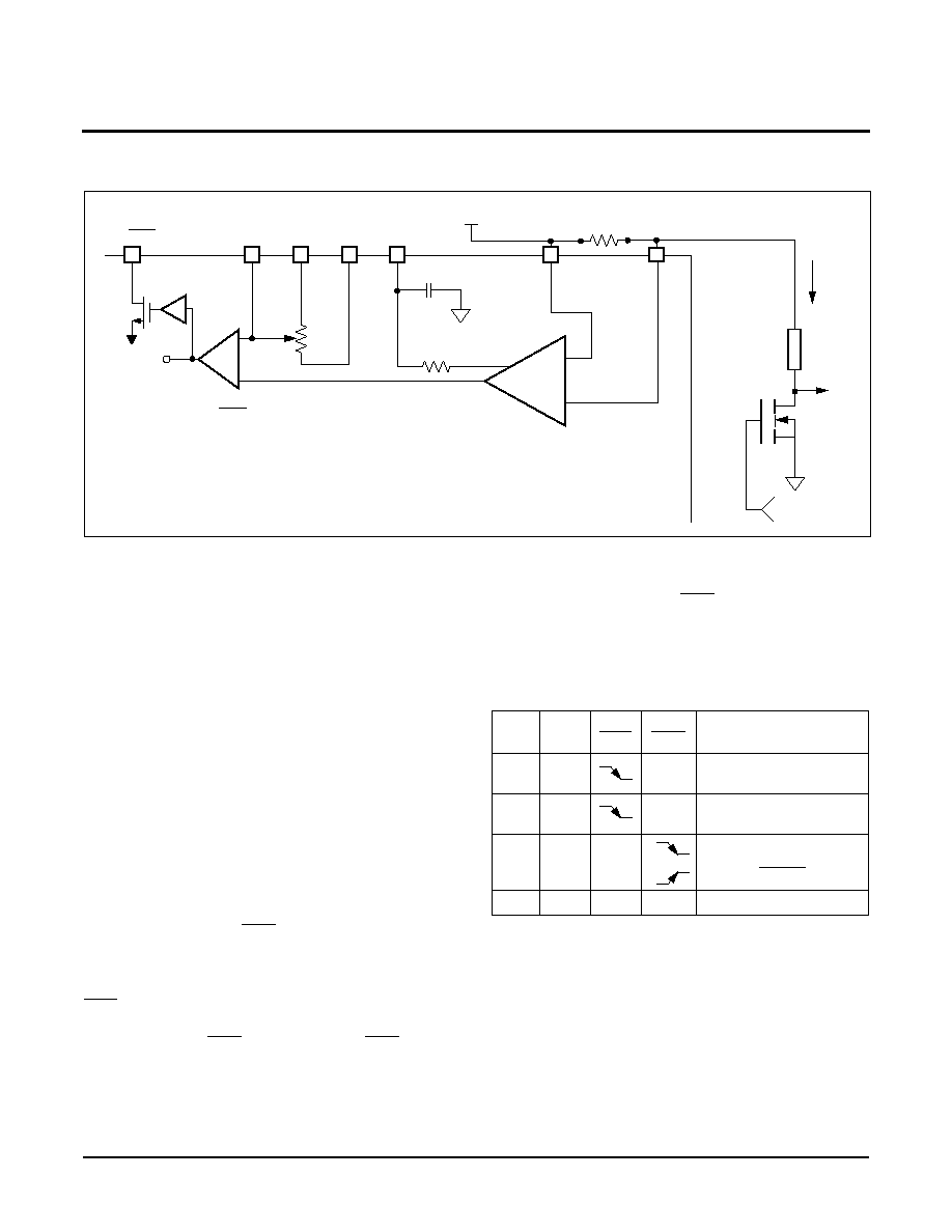
SENSE AND SCALE BLOCK
The Sense and Scale Circuit Block (Figure 2) implements
an instrumentation amplifier whose inputs (V
SENSE+
and
V
SENSE-
) are across an external sense resistor in the
drain circuit of an RF Power FET. V
SENSE+
is connected
to V
DD
, the drain voltage source for the RF power FET,
and V
SENSE-
pin is connected to the other end the exter-
nal sense resistor.
An internal instrumentation amplifier (IA) will sense the
V and amplify it by a gain factor of K
1
(see Equation
1). The resulting output is compared with V
REF
at the
comparator. V
REF
can be a fixed reference voltage or
adjusted by using the 64-tap digital potentiometer. The
output of the comparator is used to increment or decre-
ment the R
BIAS
potentiometer in the Bias Adjustment
Circuit Block. The gain factor K
1
is designed such that
the Sense and Scale Block will set the Bias Adjustment
Circuit Block to operate in a given voltage range (mV)
vs. drain current adjustment (mA).
The output of the IA is also available at the pin Vout to
enable drain current monitoring. The gain at Vout is
fixed at a factor of K
2
, lower than K
1
so that high I
DQ
currents will not cause saturation of the Vout signal.
The equation for Vout is given as:
BIAS ADJUSTMENT CIRCUIT BLOCK
There are three sections of this block (Figure 3): the
input control, counter and decode section (1), the
resistor array (2); and the non-volatile register (3). The
input control section operates just like an up/down
counter. The input of the counter is driven from the out-
put of the comparator in the Sense and Scale Block
and is clocked by the SCL signal. The output of this
counter is decoded to select one of the taps of a 256-
tap digital potentiometer.
A0
A2
VCC
VSS
V+
AGND
Comparator
choke
RF PA in
R
SENSE
V
DD
V
REF
V
SENSE+
V
BIAS
INC/DEC
Instrumentation
Amplifier
V
CS
V
OUT
V
SENSE≠
R
REF
RW
REF
RL
REF
SHDN
+
≠
EEPROM
SCL
SDA
A1
Vbias
control
VREF
control
I2C
interface
Control &
Status Registers
RF
out
RH
REF
R
BIAS
VP
RH
BIAS
RL
BIAS
RW
BIAS
FILTER
V
BIAS (Unbuffered)
RF Impedance
Matching
C
BULK
Class A Example
I
DQ
V
REF
K
1
* R
SENSE
K
1
is fixed 50x for the internal comparator input.
(1)
V = I
DQ
* R
SENSE
V
OUT
= K
2
*
V
K
2
is fixed to 20x for the Vout pin
Preliminary Information
13 of 25
REV 11.16 3/20/03
www.xicor.com
Preliminary Information
X9470
Figure 2. Sense and Scale Block Diagram
The wiper of the digital potentiometer acts like its
mechanical equivalent and does not move beyond the
last position. That is, the counter does not wrap around
when clocked to either extreme. The electronic
switches in the potentiometer operate in a "make
before break" mode when the wiper changes tap posi-
tions. If the wiper is moved several positions, multiple
taps are connected to the wiper for t
IW
(SCL to
RW
BIAS
change).
When the device is powered-up, the X9470 will load
the last saved value from the non-volatile memory into
the WCR. Note that the current wiper position can be
saved into non-volatile memory register by using the
SCL and CS pins as shown in Figure 4.
Important note: the factory setting of the wiper counter
register is the ZERO-position (0 of 255 taps). This is
the default wiper position.
Bias Adjustment Block Instructions and Program-
ming. The SCL, INC/DEC (internal signal) and CS
inputs control the movement of the wiper along the
resistor array. (See Table 1) With CS set HIGH, the
device is selected and enabled to respond to the INC/
DEC and SCL inputs. HIGH to LOW transitions on SCL
will increment or decrement R
BIAS
(depending on the
state of the INC/DEC input). The INC/DEC input is
derived from the output of the comparator of the Sense
and Scale Block.
Storing Bias Resistor Values in Memory. Wiper val-
ues are stored to VOLATILE memory automatically
when CS is HIGH and INC/DEC either transitions from
HIGH to LOW or from LOW to HIGH. Wiper values are
stored to NON-VOLATILE memory during Byte Write
or as described in the following section.
Table 1. Mode Selection
* When coming out of shutdown, the CS pin must be cycled once before bias
adjustment is enabled.
INC/DEC
RW
REF
RL
REF
RH
REF
V
OUT
V
DD
V
SENSE+
R
SENSE
V
SENSE≠
10k
64-tap
V
REF
Comparator
INC/DEC
~1kohm
Precision
I-Amp
Cint~2pF ±10%
}
V
I
DQ
RF
PA
Out
choke
V
gate
RF PA in
K
2
= 20X
K
1
= 50X
SDA
CS*
SCL
INC /
DEC
Mode
H
H
H
VBIAS is incremented
one tap position.
H
H
L
VBIAS is decremented
one tap position.
H
H
X
Lock Wiper Position.
Save to volatile
memory. (BiasLockTM)
X
L
X
X
Open Loop.
or

Preliminary Information
Preliminary Information
X9470
14 of 25
REV 11.16 3/20/03
www.xicor.com
Figure 3. Bias Adjustment Block Diagram
NON-VOLATILE STORE OF THE BIAS POSITION
The following procedure will store the values for the
Rref and Rbias wiper positions in Non-Volatile memory.
This sequence is intended to be performed after a
BiasLock calibration sequence to simplify storage. If
BiasLock has not been achieved, then the Rbias wiper
position may change when the CS pin is brought high
and SCL begins clocking. See Figure 4 for the actual
sequence.
1. Set the WEL bit with a write command (02h to regis-
ter 0Fh)
2. Peform a calibration and achieve BiasLock. Leave
CS pin high.
3. Write the address byte only (START, followed by
device/slave address and a 0 for a write, see page
20).
4. Perform a STOP command.
5. With SCL still low, bring the CS low. The falling edge
of the CS will initiate the NV write.
The WEL bit may be reset afterwards to prevent further
NV writes.
INC/DEC FUNCTION
The INC/DEC pin is an open-drain logic output that
tracks the activity of the increment/decrement compar-
ator. A logic HIGH at INC/DEC indicates that the I
DQ
did not rise up to the desired setting indicated by V
REF
while a logic LOW at the INC/DEC pin indicates that
the IDQ is higher than the desired setting.
INC/DEC is used as an internal control signal as well.
As an example, when INC/DEC is LOW, the Bias
Adjustment Circuit Block will start to move the Rbias
resistor wiper towards the RL
BIAS
terminal end when
CS is HIGH and SCL is clocking. Consequently, the
V
BIAS
voltage will decrease, and the I
DQ
decreases to
meet the desired V
REF
setting.
The INC/DEC signal can also be used to detect a dam-
aged RF power FET. For instance, If INC/DEC stays
HIGH during and after a calibration sequence it may
indicate that the RF power FET has failed. This indica-
tor can also be used with a level sense on the V
OUT
pin
to perform diagnostics.
SHUTDOWN MECHANISM
This hardware control shutdown pin (SHDN) will pull
the voltage of V
BIAS
to VSS with an internal pull down
resistor. When shutdown is disabled (V
BIAS
is active
when SHDN is LOW), the V
BIAS
voltage will move to
the previous desired bias voltage.
It will take less than a microsecond to enable the inter-
nal output buffer depending on the loading condition at
the V
BIAS
pin.
Gate Bias
Op Amp
+
≠
RW
BIAS
RH
BIAS
RL
BIAS
Legend
External pin/signal
Internal node/signal
SCL
CS
2
3
1
V
BIAS
(unbuffered)
V
BIAS
SHDN
to LDMOS gate
10Kohm
256-tap
R
BIAS
INC
U/D
CS
INC/DEC
XDCP
Memory and Control
WCR (Rbias)
Bias Register
non-volatile
Power On Recall
(POR)
Note:
1) WCR = Wiper Control Register
INC/DEC is logic HIGH or LOW
from Sense/Scale Block
and is used to increment or
decrement the Rbias resistor
(XDCP) to adjust the gate voltage.

Preliminary Information
15 of 25
REV 11.16 3/20/03
www.xicor.com
Preliminary Information
X9470
OUTPUT (V
BIAS
)
V
BIAS
is a buffered output of RW
BIAS
(wiper output). It
can deliver a high current for driving up to typically 1nF
capacitive loading with stable performance and fast
settling time.
A single pole filter should be placed in between the
V
BIAS
output and the RF input signal to isolate any
high frequency noise.
Figure 4. Non-Volatile Store of the Bias Position
X9470 PRINCIPLES OF OPERATION
The X9470 is a Bias Controller that contains all the
necessary analog components for closed-loop DC bias
control of LDMOS Transistors in RF Applications. The
X9470 provides a mechanism to periodically set DC
bias operating points of Class A or AB-type amplifiers
to account for V
GS
drift and temperature variations.
The following is an example of X9470 operation.
The X9470 incorporates an instrumentation amplifier,
comparator and buffer amplifier along with resistor
arrays and their associated registers and counters. The
serial interface provides direct communication between
the host and the X9470. This section provides a
detailed example of how the X9470 can be used to cal-
ibrate and dynamically set the optimum bias operating
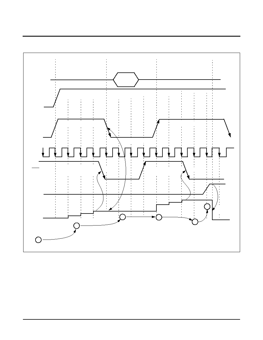
point of an RF power amplifier (see Figure 5):
≠ State 0: Power on Monitor Mode
≠ State 1: DC-bias Setting When No RF is Present
[Calibration]
≠ State 2: Calibration Disable When RF is Present
≠ State 3: PA Standby Mode. Dynamic Adjustment for
V
GS
drift and Temperature variation
≠ State 4: Power Off (Shutdown) Mode [Turn off the
Power Amplifier]
State 0: Monitor Mode
The V
OUT
and INC/DEC outputs of the X9470 can be
used for monitoring and diagnostic purposes. Since
V
OUT
has a lower gain (20x, default) than the internal IA
output, it can handle higher drain sense current while
keeping the output below the rail. This allows normal PA
power monitoring, and over-current sensing using an
external comparator. The INC/DEC pin can be moni-
tored during calibration to see if there is no change,
which indicates LDMOS functional problems. Note that
the INC/DEC status is also available in the status regis-
ter for software status reads.
State 1: DC-bias Setting When No RF is Present
[Calibration]
At calibration, the DC bias operating point of the
LDMOS Power Amplifier must be set. As soon as the
Bias Adjustment Circuit Block is enabled (CS enabled,
SDA high, and SCL pulse provided), the X9470 will
automatically calibrate the external Power Amplifier by
continually sampling the drain current of the external
Power Amplifier and make adjustments to the gate
voltage of the amplifier (See Figure 6).
Initiates
high voltage write
cycle
t
WR
Stored in
Non-volatile
memory
CS
SCL
SDA
Non-volatile Write of R
BIAS
and R
REF
value Using SDA, SCL and CS pins
R
BIAS
non-volatile register
Set WEL
bit
Calibration
and Bias Lock
Set
Address Byte
Stop
1
2
3
4
5
Preliminary Information
Preliminary Information
X9470
16 of 25
REV 11.16 3/20/03
www.xicor.com
Figure 5. Operating modes X9470
When no RF signal is present, the instrumentation
amplifier of the X9470 senses the drain current as a
voltage drop,
V, across an external drain R
sense
resis-
tor. The
V is amplified and compared to an external
scaling voltage, V
REF
. Any difference between
V and
V
REF
results in a resistive increment or decrement of
the internal R
BIAS
potentiometer.
The R
BIAS
potentiometer is used as a voltage divider
with the RH
BIAS
and RL
BIAS
terminals setting the
upper and lower voltage limits of the unbuffered
RW
BIAS
voltage. The resolution of the R
BIAS
potenti-
ometer resistor is 0.4% of the difference of voltage
across the RH
BIAS
and RL
BIAS
terminals. The R
TOTAL
is typically 10K
with 256-taps. So, for example, if the
difference between the RH
BIAS
and RL
BIAS
terminals
is 1.024V, then the step accuracy is 4mV.
The voltage at the RW
BIAS
pin is then fed into the
V
BIAS
voltage follower. The V
BIAS
pin is a buffered out-
put that is used to drive the gate of an LDMOS transis-
tor.
The scaling voltage, V
REF
, set by the R
REF
potentiom-
eter, sets the calibrated operating point of the LDMOS
Amplifier.
On edge transitions of the INC/DEC signal, the X9470 will
latch the current wiper position--this is known as "Bias
LockTM" mode. This is shown in Figure 6. When BiasLock
occurs, the comparator hysteresis will allow INC/DEC to
change state only after the IA output changes by more
than 20mV. This will prevent toggling of the V
BIAS
output
unless the drain bias current is constantly changing.
State 2: DC-bias Disable When RF is Present
(optional)
When an RF signal is present, the X9470 is put into
standby mode (open loop). The X9470 is in standby
mode when the CS pin is disabled so that the R
BIAS
potentiometer holds the last wiper position. The pres-
ence of an RF signal at the input of a Class A or AB
amplifier increases the current across the R
sense
resis-
tor. Over a period of time, the temperature of the
LDMOS also increases and the LDMOS also experi-
ences V
GS
drift. Therefore the DC biasing point that
was set during State 1 (calibration) is not optimal.
Adjustments to the gate voltage will need to be made
to optimize the operation of the LDMOS PA. This is
done in State 3.
Choose Vref to scale IDQ, perform calibration,
State 1
State 2
State 3
State 4
PA
Transmit Mode
PA
Calibration Mode
PA
Standby Mode
PA
Off Mode
Disable Bias Adjustment,
Recalibrate bias point for drift and temperature.
Rbias resistor will automatically increment or decrement
for optimal operating point continuously
Turn off PA
Latch bias point for DC bias current in wiper counter
PA Enabled, Vout and INC/DEC Monitored for status
State 0
PA
Monitor Mode

Preliminary Information
17 of 25
REV 11.16 3/20/03
www.xicor.com
Preliminary Information
X9470
State 3: PA Standby Mode, DC Bias Adjustment
[Compensation for V
GS
Drift and Temperature
Variation]
When the Power Amplifier is in Standby Mode the
X9470 allows for dynamic adjustment of the DC bias-
ing point to take into account both V
GS
drift and tem-
perature variation. Dynamic biasing is achieved with
the X9470 by using the CS, and SCL pins. For exam-
ple, the SCL pin can be a steady clock and the CS pin
can be used as a control signal to enable/disable the
Bias Adjustment Block.
Figure 6 illustrates how the X9470 can be used for
dynamic biasing. Upon the presence of an RF signal,
the CS pin is pulled LOW. This will prevent the X9470
from changing the V
BIAS
voltage during I
DQ
peak cur-
rents. Once the RF signal is no longer present, the CS
pin can be enabled (closed loop), SDA high and the
X9470 Bias Adjustment Circuit moves the V
BIAS
volt-
age (the gate voltage of the FET) to meet the average
I
DQ
bias point for optimum amplifier performance.
State 4: Power Off Mode
During power saving or power-off modes the X9470
can be shut down via the SHDN pin. This pin pulls the
output of the V
BIAS
pin LOW.
Preliminary Information
18 of 25
REV 11.16 3/20/03
www.xicor.com
Preliminary Information
X9470
Figure 6. Dynamic Biasing Technique: Automatic DC Bias Operating Point Adjustment
State 0
Monitor
Mode
State 1
Calibration
(no RF present)
State 2
RF present
State 3
Recalibrate bias
point for drift
and temperature
State 4
shut
down
Set Operating Range Scale for Bias Adjustment
RF signal
V
REF
CS
SCL
INC/DEC
SHDN
V
BIAS
1
2
3
4
5
6
R
bias
default is
zero point of R
total
Latch R
bias
DC point
in calibration vs V
REF
RF present
Turn off
Bias
Adjustment
R
bias
increase/decrease
after RF present due to
temperature increase &
V
GS
-threshold drift
IDQ vs. gate
voltage bias
optimized
Shut
down
BiasLock
Saves wiper position to
volatile memory
Bias Adjustment ON
Bias Adjustment OFF
Bias Adjustment ON
Automatic Bias Adjustment
BiasLock
Preliminary Information
19 of 25
REV 11.16 3/20/03
www.xicor.com
Preliminary Information
X9470
X9470 STATUS REGISTER (SR) AND CONTROL REGISTER (CR) INFORMATION
Table 2. Status Register (SR)
STATUS REGISTER (SR)
The Status Register is located at address 0F<hex>.
This is a register used to control the write enable
latches, and monitor status of the SHDN, INC/DEC,
and CS pin. This register is separate from the Control
Register.
SR7: SHDN: Vbias SHDN Flag. Read Only--Volatile.
The bit keeps status of the shutdown pin, SHDN. When
this bit is HIGH, the SHDN pin is active and the V
BIAS
output is disabled. When this bit is LOW, the SHDN pin
is low and V
BIAS
output is enabled.
SR6: INC/DEC : Read Only--Volatile. This bit keeps
status of the INC/DEC pin. When this bit is HIGH the
counter is in increment mode, when this bit is LOW the
counter is in decrement mode.
SR4: CS: Read Only--Volatile. This bit keeps status
on the CS pin. When this bit is HIGH, the X9470 is in
closed loop mode (Rbias adjustment enabled). When
this bit is LOW the x9470 is in open loop mode (no
Rbias adjustments).
SR2, SR3, SR5: Read only
For internal test usage, should be set to 0 during SR
writes.
SR1: WEL: Write Enable Latch--Volatile
The WEL bit controls the access to the registers during
a write operation. This bit is a volatile latch that powers
up in the LOW (disabled) state. While the WEL bit is
set LOW, Nonvolatile writes to the registers will be
ignored, and all writes to registers will be volatile. The
WEL bit is set by writing a "1" to the WEL bit and
zeroes to the other bits of the Status Register. Once
this write operation is completed and a STOP com-
mand is issued, nonvolatile writes will then occur for all
NOVRAM registers and control bits. Once set, the,
WEL bit remains set until either reset to 0 (by writing a
"0" to the WEL bit and zeroes to the other bits of the
Status Register) or until the part powers up again.
SR0: Gain - NOVRAM
Selects V
OUT
and IA gain. When SR0=0, V
OUT
gain=20x,
IA gain=50x. When SR0=1, V
OUT
gain=50x, and IA
gain=20x. Default setting is 0.
CONTROL REGISTERS (CR)
The control registers are organized for byte operations.
Each byte has a unique byte address as shown in
Table 3 below.
Table 3. Control Registers (CR)
Note:
02H to 0EH are reserved for internal manufacturing use.
Byte
Addr
SR7
SR6
SR5
SR4
SR3
SR2
SR1
SR0
0F hex
SHDN
INC/DEC
0
CS
0
0
WEL
Gain
Byte
Addr.
<HEX>
Description
Reg
Name
Bit
Memory Type
7
6
5
4
3
2
1
0
00 hex
DCP for Vbias
Vbias
Vb7
Vb6
Vb5
Vb4
Vb3
Vb2
Vb1
Vb0
NOVRAM
01 hex
DCP for
VREF
Vref
X
X
Vr5
Vr4
Vr3
Vr2
Vr1
Vr0
NOVRAM

Preliminary Information
Preliminary Information
X9470
20 of 25
REV 11.16 3/20/03
www.xicor.com
X9470 BUS INTERFACE INFORMATION
Figure 7. Slave Address, Word Address, and Data Bytes - Write Mode
Figure 8. Slave Address, Word Address, and Data Bytes - Read Mode
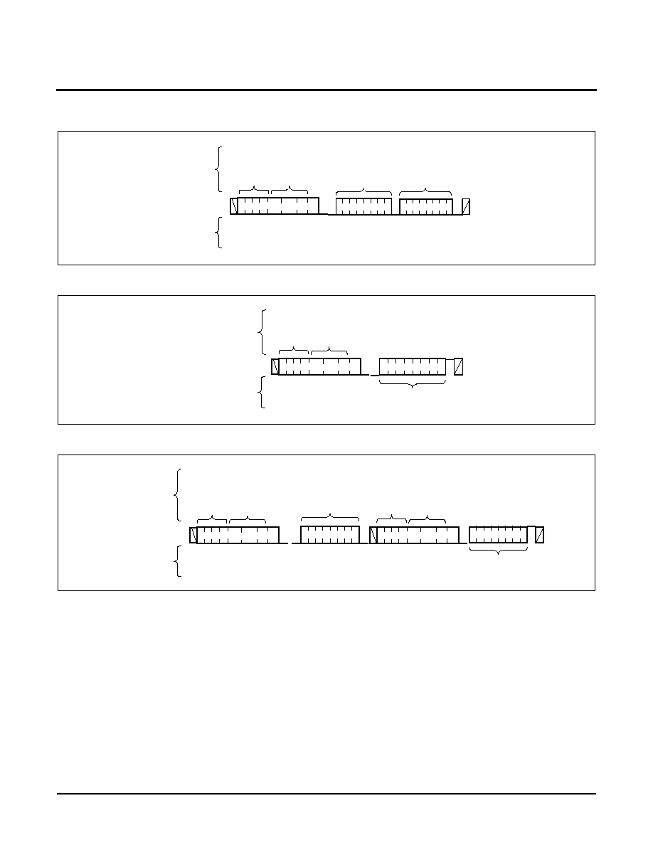
Slave Address, Byte Address, and Data Byte
The byte communication format for the serial bus is
shown in Figures 7 and 8 above. The first byte, BYTE
0, defines the device indentifier, 0101 in the upper half;
and the device slave address in the low half of the byte.
The slave address is determined by the logic values of
the A0, A1, and A2 pins of the X9470. This allows for
up to 8 unique addresses for the X9470. The next byte,
BYTE 1, is the Byte Address. The Byte Address identi-
fies a unique address for the Status or Control Regis-
ters as shown in Table 3. The following byte, Byte 2, is
the data byte that is used for READ and WRITE opera-
tions.
Start Condition
All commands are preceded by the start condition,
which is a HIGH to LOW transition of SDA when SCL is
HIGH. The device continuously monitors the SDA and
SCL lines for the start condition and will not respond to
any command until this condition has been met. See
Figure 9.
Slave Address Byte
Byte 0
D7
D6
D5
D2
D4
D3
D1
D0
A0
A7
A2
A4
A3
A1
Data Byte
Byte 2
A6
A5
0
1
0
S1
1
S0
R/W=0
S2
Device Identifier
Byte Address
Byte 1
Slave Address
0Fh : SR
00h : V
BIAS
01h : V
REF
Slave Address Byte
Byte 0
D7
D6
D5
D2
D4
D3
D1
D0
D0
D7
D2
D4
D3
D1
Data Byte
Byte 2
D6
D5
0
1
0
S1
1
S0
R/W
S2
Device Identifier
Data Byte
Byte 1
Slave Address
Preliminary Information
21 of 25
REV 11.16 3/20/03
www.xicor.com
Preliminary Information
X9470
Stop Condition
All communications must be terminated by a stop con-
dition, which is a LOW to HIGH transition of SDA when
SCL is HIGH. The stop condition is also used to place
the device into the Standby power mode after a read
sequence. A stop condition can only be issued after the
transmitting device has released the bus. See Figure 9.
Acknowledge
Acknowledge is a software convention used to indicate
successful data transfer. The transmitting device, either
master or slave, will release the bus after transmitting
eight bits. During the ninth clock cycle, the receiver will
pull the SDA line LOW to acknowledge that it received
the eight bits of data. Refer to Figure 10.
The device will respond with an acknowledge after rec-
ognition of a start condition and if the correct Device
Identifier and Select bits are contained in the Slave
Address Byte. If a write operation is selected, the
device will respond with an acknowledge after the
receipt of each subsequent eight bit word. The device
will acknowledge all incoming data and address bytes,
except for:
≠ The Slave Address Byte when the Device Identifier
and/or Select bits are incorrect
≠ The 2nd Data Byte of a Status Register Write Opera-
tion (only 1 data byte is allowed)
Figure 9. Valid Start and Stop Conditions
Figure 10. Acknowledge Response From Receiver
Figure 11. Valid Data Changes on the SDA Bus
SCL
SDA
Start
Stop
SCL from
Master
Data Output
from Transmitter
Data Output
from Receiver
8
1
9
Start
Acknowledge
SCL
SDA
Data Stable
Data Change
Data Stable

Preliminary Information
Preliminary Information
X9470
22 of 25
REV 11.16 3/20/03
www.xicor.com
WRITE OPERATIONS
Byte Write
For a write operation, the device requires the Slave
Address Byte and the Word Address Bytes. This gives
the master access to any one of the words in the array.
Upon receipt of each address byte, the X9470
responds with an acknowledge. After receiving the
address bytes the X9470 awaits the eight bits of data.
After receiving the 8 data bits, the X9470 again
responds with an acknowledge. The master then termi-
nates the transfer by generating a stop condition. The
X9470 then begins an internal write cycle of the data to
the nonvolatile memory. During the internal write cycle,
the device inputs are disabled, so the device will not
respond to any requests from the master. The SDA out-
put is at high impedance. See Figure 12.
A write to a protected block of memory is ignored, but
will still receive an acknowledge. At the end of the write
command, the X9470 will not initiate an internal write
cycle, and will continue to ACK commands.
Stops and Write Modes
Stop conditions that terminate write operations must
be sent by the master after sending at least 1 full data
byte and it's associated ACK signal. If a stop is issued
in the middle of a data byte, or before 1 full data byte +
ACK is sent, then the X9470 resets itself without per-
forming the write. The contents of the array are not
affected.
Acknowledge Polling
Disabling of the inputs during nonvolatile write cycles
can be used to take advantage of the typical 5ms write
cycle time. Once the stop condition is issued to indi-
cate the end of the master's byte load operation, the
X9470 initiates the internal nonvolatile write cycle.
Acknowledge polling can begin immediately. To do this,
the master issues a start condition followed by the
Slave Address Byte for a write or read operation. If the
X9470 is still busy with the nonvolatile write cycle then
no ACK will be returned. When the X9470 has com-
pleted the write operation, an ACK is returned and the
host can proceed with the read or write operation.
Refer to the flow chart in Figure 15.
READ OPERATIONS
There are three basic read operations: Current
Address Read, Random Read, and Sequential Read.
Current Address Read
Internally the X9470 contains an address counter that
maintains the address of the last word read incre-
mented by one. Therefore, if the last read was to
address n, the next read operation would access data
from address n+1. On power up, the address is initial-
ized to 0h. In this way, a current address read immedi-
ately after the power on reset can download the entire
contents of memory starting at the first location. Upon
receipt of the Slave Address Byte with the R/W bit set
to one, the X9470 issues an acknowledge, then trans-
mits eight data bits. The master terminates the read
operation by not responding with an acknowledge dur-
ing the ninth clock and issuing a stop condition. Refer
to Figure 13 for the address, acknowledge, and data
transfer sequence.
Preliminary Information
23 of 25
REV 11.16 3/20/03
www.xicor.com
Preliminary Information
X9470
Figure 12. Byte Write Sequence
Figure 13. Current Address Read Sequence
Figure 14. Random Address Read Sequence
S
t
a
r
t
S
t
o
p
Data
A
C
K
A
C
K
SDA Bus
Signals From
The Slave
Signals from
the Master
0
A
C
K
Byte
Address 0
A0
A1
A2
0
1
0
1
Slave
Address
Device
ID
S
t
a
r
t
S
t
o
p
Data
A
C
K
SDA Bus
Signals from
the Slave
Signals from the
Master
Slave
Address
1
A0
A1
A2
0
1
0
1
Device
ID
A
C
K
A
C
K
S
t
a
r
t
S
t
o
p
Data
S
t
a
r
t
SDA Bus
Signals from
the Slave
Signals from the
Master
Byte
Address 0
A
C
K
Slave
Address
0
A0
A1
A2
0
1
0
1
Device
ID
A
C
K
Slave
Address
1
A0
A1
A2
0
1
0
1
Device
ID
A
C
K

Preliminary Information
Preliminary Information
X9470
24 of 25
REV 11.16 3/20/03
www.xicor.com
Figure 15. Acknowledge Polling Sequence
It should be noted that the ninth clock cycle of the read
operation is not a "don't care." To terminate a read
operation, the master must either issue a stop condi-
tion during the ninth cycle or hold SDA HIGH during
the ninth clock cycle and then issue a stop condition.
Random Read
Random read operations allows the master to access
any location in the X9470. Prior to issuing the Slave
Address Byte with the R/W bit set to zero, the master
must first perform a "dummy" write operation.
The master issues the start condition and the slave
address byte, receives an acknowledge, then issues
the word address bytes. After acknowledging receipt of
each word address byte, the master immediately
issues another start condition and the slave address
byte with the R/W bit set to one. This is followed by an
acknowledge from the device and then by the eight bit
data word. The master terminates the read operation
by not responding with an acknowledge and then issu-
ing a stop condition. Refer to Figure 13 for the address,
acknowledge, and data transfer sequence.
In a similar operation called "Set Current Address," the
device sets the address if a stop is issued instead of
the second start shown in Figure 14. The X9470 then
goes into standby mode after the stop and all bus
activity will be ignored until a start is detected. This
operation loads the new address into the address
counter. The next Current Address Read operation will
read from the newly loaded address. This operation
could be useful if the master knows the next address it
needs to read, but is not ready for the data.
ACK
returned?
Issue Slave
Address Byte
(Read or Write)
Byte load completed
by issuing STOP.
Enter ACK Polling
Issue STOP
Issue START
NO
YES
Issue STOP
NO
Continue normal
Read or Write
command
sequence
PROCEED
YES
nonvolatile write
Cycle complete.
Continue command
sequence?

Preliminary Information
Characteristics subject to change without notice.
25 of 25
LIMITED WARRANTY
Devices sold by Xicor, Inc. are covered by the warranty and patent indemnification provisions appearing in its Terms of Sale only. Xicor, Inc. makes no warranty,
express, statutory, implied, or by description regarding the information set forth herein or regarding the freedom of the described devices from patent infringement.
Xicor, Inc. makes no warranty of merchantability or fitness for any purpose. Xicor, Inc. reserves the right to discontinue production and change specifications and prices
at any time and without notice.
Xicor, Inc. assumes no responsibility for the use of any circuitry other than circuitry embodied in a Xicor, Inc. product. No other circuits, patents, or licenses are implied.
TRADEMARK DISCLAIMER:
Xicor and the Xicor logo are registered trademarks of Xicor, Inc. AutoStore, Direct Write, Block Lock, SerialFlash, MPS, BiasLock and XDCP are also trademarks of
Xicor, Inc. All others belong to their respective owners.
U.S. PATENTS
Xicor products are covered by one or more of the following U.S. Patents: 4,326,134; 4,393,481; 4,404,475; 4,450,402; 4,486,769; 4,488,060; 4,520,461; 4,533,846;
4,599,706; 4,617,652; 4,668,932; 4,752,912; 4,829,482; 4,874,967; 4,883,976; 4,980,859; 5,012,132; 5,003,197; 5,023,694; 5,084,667; 5,153,880; 5,153,691;
5,161,137; 5,219,774; 5,270,927; 5,324,676; 5,434,396; 5,544,103; 5,587,573; 5,835,409; 5,977,585. Foreign patents and additional patents pending.
LIFE RELATED POLICY
In situations where semiconductor component failure may endanger life, system designers using this product should design the system with appropriate error detection
and correction, redundancy and back-up features to prevent such an occurrence.
Xicor's products are not authorized for use in critical components in life support devices or systems.
1. Life support devices or systems are devices or systems which, (a) are intended for surgical implant into the body, or (b) support or sustain life, and whose failure to
perform, when properly used in accordance with instructions for use provided in the labeling, can be reasonably expected to result in a significant injury to the user.
2. A critical component is any component of a life support device or system whose failure to perform can be reasonably expected to cause the failure of the life
support device or system, or to affect its safety or effectiveness.
©Xicor, Inc. 2003 Patents Pending
REV 11.16 3/20/03
www.xicor.com
Preliminary Information
X9470
PACKAGING INFORMATION
NOTE: ALL DIMENSIONS IN INCHES (IN PARENTHESES IN MILLIMETERS)
24-Lead Plastic, TSSOP Package Type V
.169 (4.3)
.177 (4.5)
.252 (6.4) BSC
.026 (.65) BSC
.303 (7.70)
.311 (7.90)
.002 (.06)
.005 (.15)
.047 (1.20)
.0075 (.19)
.0118 (.30)
See Detail "A"
.031 (.80)
.041 (1.05)
0
∞ ≠ 8∞
.010 (.25)
.020 (.50)
.030 (.75)
Gage Plane
Seating Plane
Detail A (20X)