 | –≠–ª–µ–∫—Ç—Ä–æ–Ω–Ω—ã–π –∫–æ–º–ø–æ–Ω–µ–Ω—Ç: XC3090 | –°–∫–∞—á–∞—Ç—å:  PDF PDF  ZIP ZIP |

2-103
Æ
XC3000 Logic Cell Array Families
Overview .............................................................. 2-104
XC3000, XC3000A, XC3000L, XC3100, XC3100A
Logic Cell Array Families ................................. 2-105
Architecture ...................................................... 2-106
Programmable Interconnect ............................. 2-111
Crystal Oscillator .............................................. 2-117
Programming ................................................... 2-118
Special Configuration Functions ...................... 2-122
Master Serial Mode .......................................... 2-124
Master Serial Mode Programming
Switching Characteristics ............................. 2-125
Master Parallel Mode ....................................... 2-126
Master Parallel Mode Programming
Switching Characteristics ............................. 2-127
Peripheral Mode ............................................... 2-128
Peripheral Mode Programming
Switching Characteristics ............................. 2-129
Slave Serial Mode ............................................ 2-130
Slave Serial Mode Programming
Switching Characteristics ............................. 2-131
Program Readback Switching
Characteristics ............................................. 2-131
General LCA Switching Characteristics ........... 2-132
Performance .................................................... 2-133
Power ............................................................... 2-134
Pin Descriptions ............................................... 2-136
Pin Functions During Configuration.................. 2-138
XC3000 Families Pin Assignments .................. 2-139
XC3000 Families Pinouts ................................. 2-140
Component Availability ..................................... 2-151
Ordering Information ........................................ 2-152
XC3000 Logic Cell Array Family ........................... 2-153
Absolute Maximum Ratings ............................. 2-154
Operating Conditions ....................................... 2-154
DC Characteristics ........................................... 2-155
Switching Characteristic Guidelines
CLB .............................................................. 2-156
Buffer ........................................................... 2-156
IOB .............................................................. 2-158
Ordering Information ........................................ 2-160
Component Availability ..................................... 2-160
Table of Contents
XC3000A Logic Cell Array Familiy ....................... 2-161
Absolute Maximum Ratings ............................. 2-162
Operating Conditions ....................................... 2-162
DC Characteristics ........................................... 2-163
Switching Characteristic Guidelines
CLB .............................................................. 2-164
Buffer ........................................................... 2-164
IOB .............................................................. 2-166
Ordering Information ........................................ 2-168
Component Availability ..................................... 2-168
XC3000L Low Voltage Logic Cell Array Family .... 2-169
Absolute Maximum Ratings ............................. 2-170
Operating Conditions ....................................... 2-170
DC Characteristics ........................................... 2-171
Switching Characteristic Guidelines
CLB .............................................................. 2-172
Buffer ........................................................... 2-172
IOB .............................................................. 2-174
Ordering Information ........................................ 2-176
Component Availability ..................................... 2-176
XC3100, XC3100A Logic Cell Array Families ....... 2-177
Absolute Maximum Ratings ............................. 2-178
Operating Conditions ....................................... 2-178
DC Characteristics ........................................... 2-179
Switching Characteristic Guidelines
CLB .............................................................. 2-180
Buffer ........................................................... 2-180
IOB .............................................................. 2-182
Ordering Information ........................................ 2-184
Component Availability ..................................... 2-184

XC3000, XC3000A, XC3000L, XC3100, XC3100A Logic Cell Array Families
2-104
Overview
Introduced in 1987/88, XC3000 is the industry's most
successful family of FPGAs, with over 10 million devices
shipped. In 1992/93, Xilinx introduced three additional
families, offering more speed, functionality, and a new
supply-voltage option.
There are now five distinct family groupings within the
XC3000 class of LCA devices.
∑ XC3000 Family
∑ XC3000A Family (use for new designs)
∑ XC3000L Family (use for new designs)
∑ XC3100 Family
∑ XC3100A Family (use for new designs)
All five families share a common architecture, develop-
ment software, design and programming methodology,
and also common package pin-outs. An extensive Product
Description covers these common aspects. (Page 2-99).
The much shorter individual Product Specifications then
provide detailed parametric information for the four indi-
vidual product families.
Here is a simple overview.
XC3000 Family
The basic XC3000 family forms the cornerstone for the
rest of the XC3000 class of devices. The basic XC3000
family offers five different device densities with guaran-
teed toggle rates from 70 to 125 MHz.
XC3000A Family
The XC3000A is an enhanced version of the basic XC3000
family, featuring additional interconnect resources and
other user-friendly enhancements. The ease-of-use of the
XC3000A family makes it the obvious choice for all new
designs that do not require the speed of the XC3100 or the
3-V operation of the XC3000L.
XC3000L Family
The XC3000L is identical in architecture and features to
the XC3000A family, but operates at a nominal supply
voltage of 3.3 V. The XC3000L is the right solution for
battery-operated and low-power applications.
XC3100 Family
The XC3100 is a performance-optimized relative of the
basic XC3000 family. While both families are bitstream
and footprint compatible, the XC3100 family extends toggle
rates to 270 MHz and in-system performance to 80 MHz.
The XC3100 family also offers one additional array size,
the XC3195. The XC3100 is best suited for designs that
require the highest clock speed or the shortest net delays.
XC3100A Family
The XC3100A combines the enhanced feature set of the
XC3000A with the performance of the XC3100. It offers the
highest functionality, speed and capacity of all XC3000
families.
The figure below illustrates the relationships between the
families. Compared to the original XC3000 family, XC3000A
offers additional functionality and , coming soon, increased
speed. The XC3000L family offers the same additional
functionality, but reduced speed due to its lower supply
voltage of 3.3 V. The XC3100 family offers no additional
functionality, but substantially higher speed, and higher
density with its new member, the XC3195.
XC3195
Gate Capacity
X3447
Functionality
XC3000L
XC3000A
XC3000
XC3100
Speed
XC3100A
2-105
XC3000,
XC3000A, XC3000L,
XC3100, XC3100A
Logic Cell
Array Families
Æ
Features
∑
Complete line of five related Field Programmable
Gate Array product families
≠ XC3000, XC3000A, XC3000L, XC3100, XC3100A
∑
Ideal for a wide range of custom VLSI design tasks
≠ Replaces TTL, MSI, and other PLD logic
≠ Integrates complete sub-systems into a single
package
≠ Avoids the NRE, time delay, and risk of
conventional masked gate arrays
∑
High-performance CMOS static memory technology
≠ Guaranteed toggle rates of 70 to 325 MHz, logic
delays from 9 to 2.2 ns
≠ System clock speeds over 80 MHz
≠ Low quiescent and active power consumption
∑
Flexible FPGA architecture
≠ Compatible arrays ranging from 1,000 to 7,500
gate complexity
≠ Extensive register, combinatorial, and I/O
capabilities
≠ High fan-out signal distribution, low-skew clock
nets
≠ Internal 3-state bus capabilities
≠ TTL or CMOS input thresholds
≠ On-chip crystal oscillator amplifier
∑
Unlimited reprogrammability
≠ Easy design iteration
≠ In-system logic changes
∑
Extensive Packaging Options
≠ Over 20 different packages
≠ Plastic and ceramic surface-mount and pin-grid-
array packages
≠ Thin and Very Thin Quad Flat Pack (TQFP and
VQFP) options
∑
Ready for volume production
≠ Standard, off-the-shelf product availability
≠ 100% factory pre-tested devices
≠ Excellent reliability record
∑
Complete XACT Development System
≠ Schematic capture, automatic place and route
≠ Logic and timing simulation
≠ Interactive design editor for design optimization
≠ Timing calculator
≠ Interfaces to popular design environments like
Viewlogic, Cadence, Mentor Graphics, and others
Description
The CMOS XC3000 Class of Logic Cell Array (LCA)
families provide a group of high-performance, high-den-
sity, digital integrated circuits. Their regular, extendable,
flexible, user-programmable array architecture is com-
posed of a configuration program store plus three types of
configurable elements: a perimeter of I/O Blocks (IOBs), a
core array of Configurable Logic Bocks (CLBs) and re-
sources for interconnection. The general structure of an
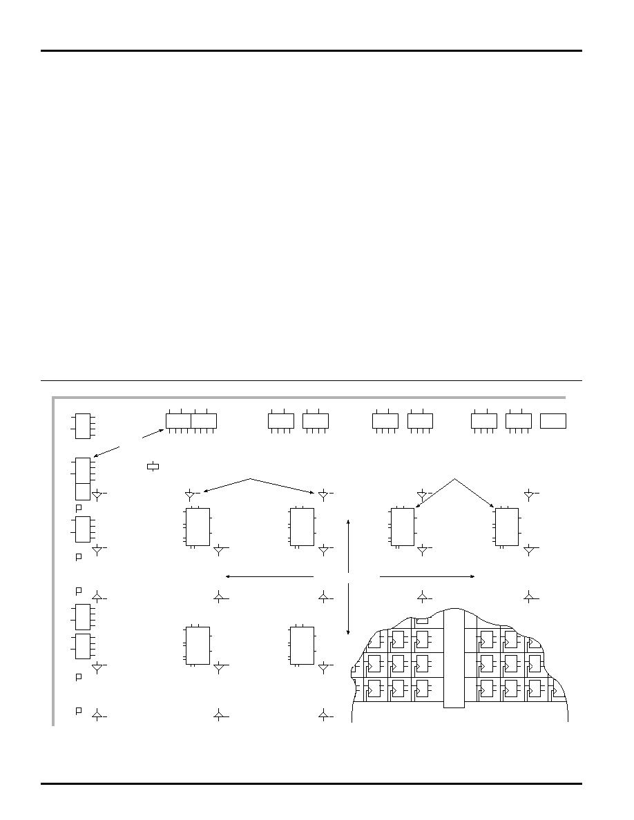
LCA device is shown in Figure 1 on the next page. The
XACT development system provides schematic capture
and auto place-and-route for design entry. Logic and
timing simulation, and in-circuit emulation are available as
design verification alternatives. The design editor is used
for interactive design optimization, and to compile the data
pattern that represents the configuration program.
The LCA user logic functions and interconnections are
determined by the configuration program data stored in
internal static memory cells. The program can be loaded in
any of several modes to accommodate various system
requirements. The program data resides externally in an
EEPROM, EPROM or ROM on the application circuit
board, or on a floppy disk or hard disk. On-chip initialization
logic provides for optional automatic loading of program
data at power-up. The companion XC17XX Serial
Configuration PROMs provide a very simple serial config-
uration program storage in a one-time programmable
package.
User I/Os
Horizontal
Configuration
Device
CLBs
Array
Max
Flip-Flops
Longlines
Data Bits
XC3020, 3020A, 3020L, 3120, 3120A
64
8 x 8
64
256
16
14,779
XC3030, 3030A, 3030L, 3130, 3130A
100
10 x 10
80
360
20
22,176
XC3042, 3042A, 3042L, 3142, 3142A
144
12 x 12
96
480
24
30,784
XC3064, 3064A, 3064L, 3164, 3164A
224
16 x 14
120
688
32
46,064
XC3090, 3090A, 3090L, 3190, 3190A
320
16 x 20
144
928
40
64,160
XC3195, 3195A
484
22 x 22
176
1,320
44
94,984
Product Description
IMPORTANT NOTICE
All new designs should use XC3000A or
XC3100A. Information on XC3000 and
XC3100 is presented here as reference
for existing designs.
XC3000, XC3000A, XC3000L, XC3100, XC3100A Logic Cell Array Families
2-106
P9
P8
P7
P6
P5
P4
P3
P2
GND
PWR
DN
P11
P12
P13
U61
TCL
KIN
AD
AC
AB
AA
3-State Buffers With Access
to Horizontal Long Lines
Configurable Logic
Blocks
Interconnect Area
BB
BA
Frame Pointer
Configuration Memory
I/O Blocks
X3241
Figure 1. Logic Cell Array Structure.
It consists of a perimeter of programmable I/O blocks, a core of configurable logic blocks and their interconnect resources.
These are all controlled by the distributed array of configuration program memory cells.
The XC3000 Logic Cell Array families provide a variety of
logic capacities, package styles, temperature ranges and
speed grades.
Architecture
The perimeter of configurable IOBs provides a pro-
grammable interface between the internal logic array and
the device package pins. The array of CLBs performs
user-specified logic functions. The interconnect resources
are programmed to form networks, carrying logic signals
among blocks, analogous to printed circuit board traces
connecting MSI/SSI packages.
The block logic functions are implemented by programmed
look-up tables. Functional options are implemented by
program-controlled multiplexers. Interconnecting networks
between blocks are implemented with metal segments
joined by program-controlled pass transistors.
These LCA functions are established by a configuration
program which is loaded into an internal, distributed array
of configuration memory cells. The configuration program
is loaded into the LCA device at power-up and may be
reloaded on command. The Logic Cell Array includes logic
and control signals to implement automatic or passive
configuration. Program data may be either bit serial or byte
parallel. The XACT development system generates the
configuration program bitstream used to configure the
LCA device. The memory loading process is independent
of the user logic functions.
Configuration Memory
The static memory cell used for the configuration memory
in the Logic Cell Array has been designed specifically for
high reliability and noise immunity. Integrity of the LCA
device configuration memory based on this design is
assured even under adverse conditions. Compared with
other programming alternatives, static memory provides
the best combination of high density, high performance,
high reliability and comprehensive testability. As shown in
Figure 2, the basic memory cell consists of two CMOS
inverters plus a pass transistor used for writing and read-
ing cell data. The cell is only written during configuration
and only read during readback. During normal operation,
the cell provides continuous control and the pass transistor
is off and does not affect cell stability. This is quite different
from the operation of conventional memory devices, in
which the cells are frequently read and rewritten.
2-107
The method of loading the configuration data is selectable.
Two methods use serial data, while three use byte-wide
data. The internal configuration logic utilizes framing
information, embedded in the program data by the XACT
development system, to direct memory-cell loading. The
serial-data framing and length-count preamble provide
programming compatibility for mixes of various LCA device
devices in a synchronous, serial, daisy-chain fashion.
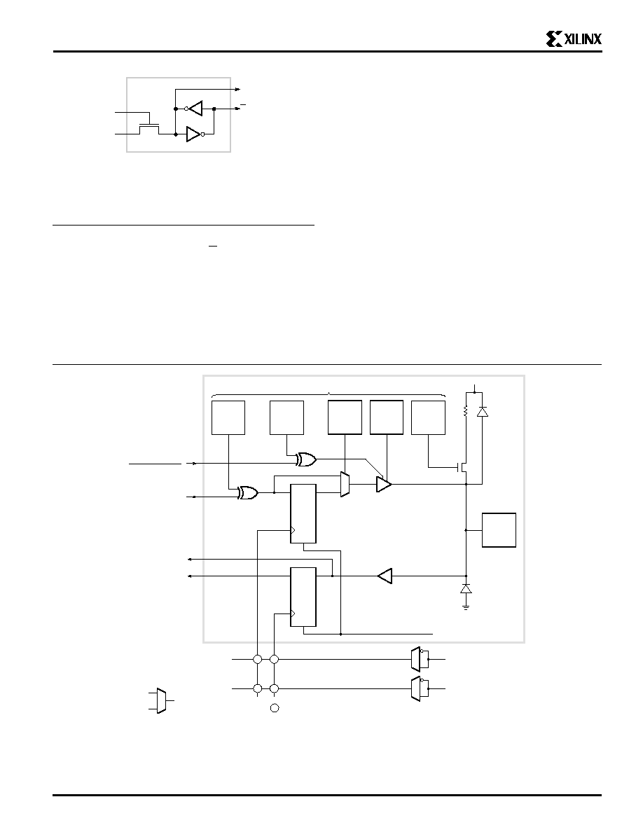
I/O Block
Each user-configurable IOB shown in Figure 3, provides
an interface between the external package pin of the
device and the internal user logic. Each IOB includes both
registered and direct input paths. Each IOB provides a
programmable 3-state output buffer, which may be driven
by a registered or direct output signal. Configuration
options allow each IOB an inversion, a controlled slew rate
and a high impedance pull-up. Each input circuit also
provides input clamping diodes to provide electrostatic
protection, and circuits to inhibit latch-up produced by
input currents.
FLIP
FLOP
Q
D
R
SLEW
RATE
PASSIVE
PULL UP
OUTPUT
SELECT
3-STATE
INVERT
OUT
INVERT
FLIP
FLOP
or
LATCH
D
Q
R
REGISTERED IN
DIRECT IN
OUT
3- STATE
(OUTPUT ENABLE)
TTL or
CMOS
INPUT
THRESHOLD
OUTPUT
BUFFER
(GLOBAL RESET)
CK1
X3029
I/O PAD
Vcc
PROGRAM-CONTROLLED MEMORY CELLS
PROGRAMMABLE INTERCONNECTION POINT or PIP
=
IK
OK
Q
I
O
T
PROGRAM
CONTROLLED
MULTIPLEXER
CK2
Figure 3. Input/Output Block.
Each IOB includes input and output storage elements and I/O options selected by configuration memory cells. A choice of two
clocks is available on each die edge. The polarity of each clock line (not each flip-flop or latch) is programmable. A clock line that
triggers the flip-flop on the rising edge is an active Low Latch Enable (Latch transparent) signal and vice versa. Passive pull-up can
only be enabled on inputs, not on outputs. All user inputs are programmed for TTL or CMOS thresholds.
Figure 2. Static Configuration Memory Cell.
It is loaded with one bit of configuration program and
controls one program selection in the Logic Cell Array.
The memory cell outputs Q and Q use ground and V
CC
levels and provide continuous, direct control. The addi-
tional capacitive load together with the absence of address
decoding and sense amplifiers provide high stability to the
cell. Due to the structure of the configuration memory cells,
they are not affected by extreme power-supply excursions
or very high levels of alpha particle radiation. In reliability
testing, no soft errors have been observed even in the
presence of very high doses of alpha radiation.
Q
Data
Read or
Write
Configuration
Control
Q
X5382