
APPLICATION NOTE
DS045 (v1.1) February 10, 2000
www.xilinx.com
1
1-800-255-7778
Features
∑
Industry's first TotalCMOSTM PLD - both CMOS design
and process technologies
∑
Fast Zero Power (FZPTM) design technique provides
ultra-low power and very high speed
∑
High speed pin-to-pin delays of 6 ns
∑
Ultra-low static power of less than 75
µ
A
∑
100% routable with 100% utilization while all pins and
all macrocells are fixed
∑
Deterministic timing model that is extremely simple to
use
∑
Two clocks with programmable polarity at every
macrocell
∑
Support for asynchronous clocking
∑
Innovative XPLATM
architecture combines high speed
with extreme flexibility
∑
1000 erase/program cycles guaranteed
∑
20 years data retention guaranteed
∑
Logic expandable to 37 product terms
∑
PCI compliant
∑
Advanced 0.5
µ
E
2
CMOS process
∑
Security bit prevents unauthorized access
∑
Design entry and verification using industry standard
and Xilinx CAE tools
∑
Reprogrammable using industry standard device
programmers
∑
Innovative Control Term structure provides either sum
terms or product terms in each logic block for:
-
Programmable 3-state buffer
-
Asynchronous macrocell register preset/reset
∑
Programmable global 3-state pin facilitates `bed of
nails' testing without using logic resources
∑
Available in both PLCC and VQFP packages
∑
Available in both Commercial and Industrial grades
Description
The XCR5032 CPLD (Complex Programmable Logic
Device) is the first in a family of CoolRunnerTM CPLDs from
Xilinx. These devices combine high speed and zero power
in a 32 macrocell CPLD. With the FZP design technique,
the XCR5032 offers true pin-to-pin speeds of 6 ns, while
simultaneously delivering power that is less than 75
µ
A at
standby without the need for "turbo bits" or other power
down schemes. By replacing conventional sense amplifier
methods for implementing product terms (a technique that
has been used in PLDs since the bipolar era) with a cas-
caded chain of pure CMOS gates, the dynamic power is
also substantially lower than any competing CPLD. These
devices are the first TotalCMOS PLDs, as they use both a
CMOS process technology and the patented full CMOS
FZP design technique. For 3V applications, Xilinx also
offers the high speed XCR3032 CPLD that offers these fea-
tures in a full 3V implementation.
The Xilinx FZP CPLDs utilize the patented XPLA
(eXtended Programmable Logic Array) architecture. The
XPLA architecture combines the best features of both PLA
and PAL type structures to deliver high speed and flexible
logic allocation that results in superior ability to make
design changes with fixed pinouts. The XPLA structure in
each logic block provides a fast 6 ns PAL path with five ded-
icated product terms per output. This PAL path is joined by
an additional PLA structure that deploys a pool of 32 prod-
uct terms to a fully programmable OR array that can allo-
cate the PLA product terms to any output in the logic block.
This combination allows logic to be allocated efficiently
throughout the logic block and supports as many as 37
product terms on an output. The speed with which logic is
allocated from the PLA array to an output is only 2 ns,
regardless of the number of PLA product terms used, which
results in worst case t
PD
's of only 8 ns from any pin to any
other pin. In addition, logic that is common to multiple out-
puts can be placed on a single PLA product term and
shared across multiple outputs via the OR array, effectively
increasing design density.
The XCR5032 CPLDs are supported by industry standard
CAE tools (Cadence/OrCAD, Exemplar Logic, Mentor, Syn-
opsys, Synario, Viewlogic, and Synplicity), using text
(ABEL, VHDL, Verilog) and/or schematic entry. Design ver-
ification uses industry standard simulators for functional
and timing simulation. Development is supported on per-
sonal computer, Sparc, and HP platforms. Device fitting
uses a Xilinx developed tool, XPLA Professional (available
on the Xilinx web site).
The XCR5032 CPLD is reprogrammable using industry
standard device programmers from vendors such as Data
I/O, BP Microsystems, SMS, and others.
0
XCR5032: 32 Macrocell CPLD
DS045 (v1.1) February 10, 2000
0
14*
Product Specification
R
xcr5032.fm Page 1 Tuesday, February 15, 2000 3:43 PM

R
XCR5032: 32 Macrocell CPLD
DS045 (v1.1) February 10, 2000
www.xilinx.com
2
1-800-255-7778
XPLA Architecture
Figure 1
shows a high level block diagram of a 32 macrocell
device implementing the XPLA architecture. The XPLA
architecture consists of logic blocks that are interconnected
by a Zero-power Interconnect Array (ZIA). The ZIA is a vir-
tual crosspoint switch. Each logic block is essentially a
36V16 device with 36 inputs from the ZIA and 16 macro-
cells. Each logic block also provides 32 ZIA feedback paths
from the macrocells and I/O pins.
From this point of view, this architecture looks like many
other CPLD architectures. What makes the CoolRunner
family unique is what is inside each logic block and the
design technique used to implement these logic blocks.
The contents of the logic block will be described next.
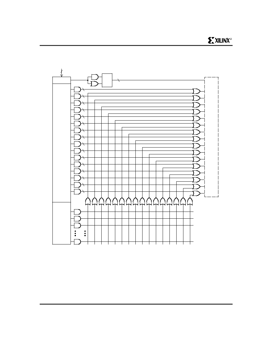
Logic Block Architecture
Figure 2
illustrates the logic block architecture. Each logic
block contains control terms, a PAL array, a PLA array, and
16 macrocells. the six control terms can individually be con-
figured as either SUM or PRODUCT terms, and are used to
control the preset/reset and output enables of the 16 mac-
rocells' flip-flops. The PAL array consists of a programma-
ble AND array with a fixed OR array, while the PLA array
consists of a programmable AND array with a programma-
ble OR array. The PAL array provides a high speed path
through the array, while the PLA array provides increased
product term density.
Each macrocell has five dedicated product terms from the
PAL array. The pin-to-pin t
PD
of the XCR5032 device
through the PAL array is 6 ns. This performance is equiva-
lent to the fastest 5V CPLD available today. If a macrocell
needs more than five product terms, it simply gets the addi-
tional product terms from the PLA array. The PLA array
consists of 32 product terms, which are available for use by
all 16 macrocells. The additional propagation delay
incurred by a macrocell using one or all 32 PLA product
terms is just 2 ns. So the total pin-to-pin t
PD
for the
XCR5032 using six to 37 product terms is 8 ns (6 ns for the
PAL + 2 ns for the PLA).
SP00550
LOGIC
BLOCK
I/O
36
16
16
36
16
16
MC0
MC1
MC15
I/O
MC0
MC1
MC15
ZIA
LOGIC
BLOCK
Figure 1: Xilinx XPLA CPLD Architecture
xcr5032.fm Page 2 Tuesday, February 15, 2000 3:43 PM
R
XCR5032: 32 Macrocell CPLD
3
www.xilinx.com
DS045 (v1.1) February 10, 2000
1-800-255-7778
T
O
16 MA
CR
OCELLS
6
5
CONTROL
PAL
ARRAY
36 ZIA INPUTS
PLA
ARRAY
(32)
SP00435A
Figure 2: Xilinx XPLA Logic Block Architecture
xcr5032.fm Page 3 Tuesday, February 15, 2000 3:43 PM
R
XCR5032: 32 Macrocell CPLD
DS045 (v1.1) February 10, 2000
www.xilinx.com
4
1-800-255-7778
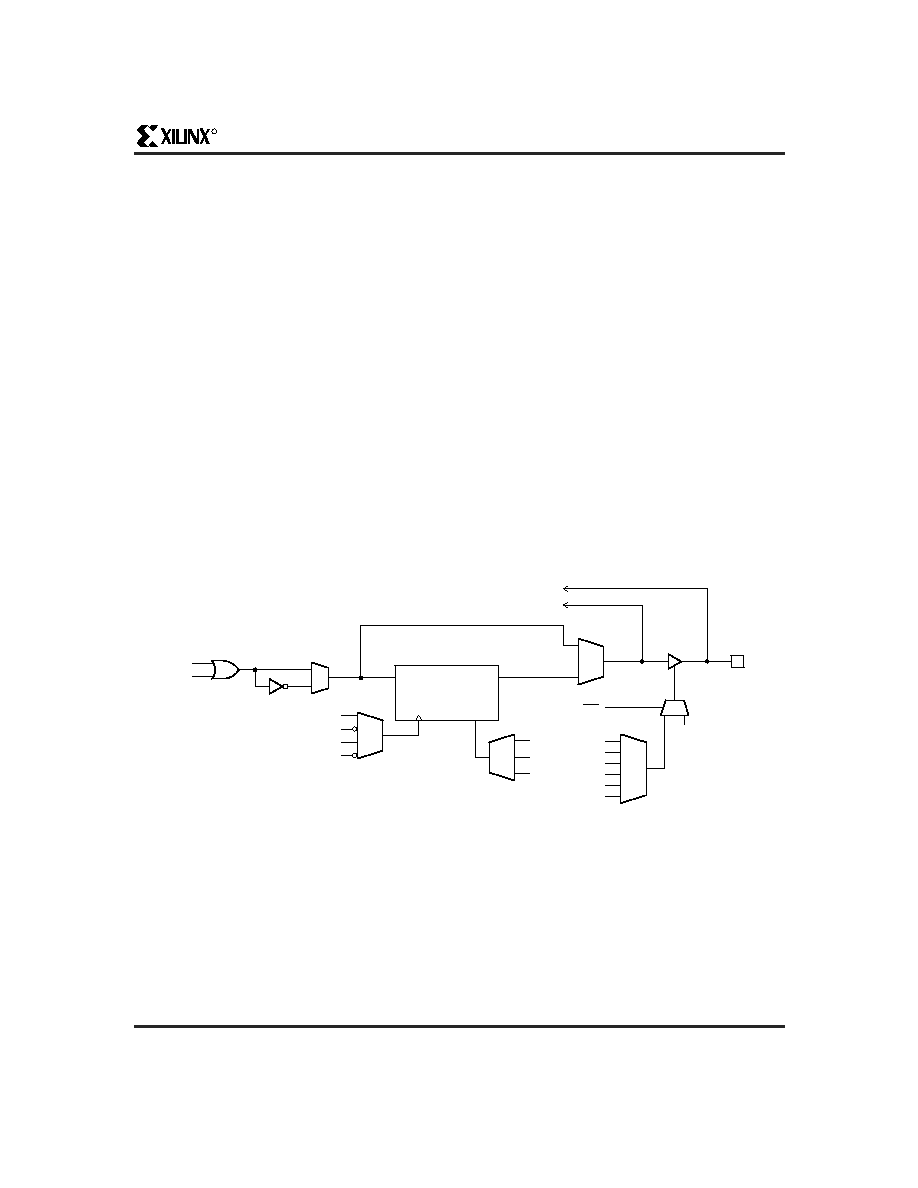
Macrocell Architecture
Figure 2
shows the architecture of the macrocell used in
the CoolRunner family. The macrocell consists of a flip-flop
that can be configured as either a D- or T-type. A D-type
flip-flop is generally more useful for implementing state
machines and data buffering. A T-type flip-flop is generally
more useful in implementing counters. All CoolRunner fam-
ily members provide both synchronous and asynchronous
clocking and provide the ability to clock off either the falling
or rising edges of these clocks. These devices are
designed such that the skew between the rising and falling
edges of a clock are minimized for clocking integrity. There
are two clocks (CLK0 and CLK1) available on the XCR5032
device. Clock 0 (CLK0) is designated as the "synchronous"
clock and must be driven by an external source. Clock 1
(CLK1) can either be used as a synchronous clock (driven
by an external source) or as an asynchronous clock (driven
by a macrocell equation). The timing for asynchronous
clocks is different in that the t
CO
time is extended by the
amount of time that it takes for the signal to propagate
through the array and reach the clock network, and the t
SU
time is reduced.
Two of the control terms (CT0 and CT1) are used to control
the Preset/Reset of the macrocell's flip-flop. The Pre-
set/Reset feature for each macrocell can also be disabled.
Note that the Power-on Reset leaves all macrocells in the
"zero" state when power is properly applied. The other four-
control terms (CT2-CT5) can be used to control the Output
Enable of the macrocell's output buffers. The reason there
are as many control terms dedicated for the Output Enable
of the macrocell is to insure that all CoolRunner devices are
PCI compliant. The macrocell's output buffers can also be
always enabled or disabled. All CoolRunner devices also
provide a Global 3-State (GTS) pin, which, when enabled
and pulled Low, will 3-state all the outputs of the device.
This pin is provided to support "In-Circuit Testing" or
"Bed-of-Nails" testing.
There are two feedback paths to the ZIA: one from the mac-
rocell, and one from the I/O pin. The ZIA feedback path
before the output buffer is the macrocell feedback path,
while the ZIA feedback path after the output buffer is the I/O
pin ZIA path. When the macrocell is used as an output, the
output buffer is enabled, and the macrocell feedback path
can be used to feedback the logic implemented in the mac-
rocell. When the I/O pin is used as an input, the output
buffer will be 3-stated and the input signal will be fed into
the ZIA via the I/O feedback path, and the logic imple-
mented in the buried macrocell can be fed back to the ZIA
via the macrocell feedback path. It should be noted that
unused inputs or I/Os should be properly terminated.
Terminations
The CoolRunner XCR5032C CPLDs are TotalCMOS
devices. As with other CMOS devices, it is important to
consider how to properly terminate unused inputs and I/O
pins when fabricating a PC board. The XCR5032C devices
do not have on-chip termination circuits, so it is recom-
mended that unused inputs and I/O pins be properly termi-
nated. Allowing unused inputs and I/O pins to float can
cause the voltage to be in the linear region of the CMOS
input structures, which can increase the power consump-
tion of the device. Xilinx recommends the use of 10K
pull-up resistors for the termination. Using pull-up resistors
allows the flexibility of using these pins should late design
changes require additional I/O. These unused pins may
also be tied directly to V
CC
, but this will make it more diffi-
cult to reclaim the use of the pin, should this be needed by
a subsequent design revision.See the application note Ter-
minating Unused I/O Pins in Xilinx XPLA1 and XPLA2
CoolRunner CPLDs for more information.
Figure 2: XCR5032 Macrocell Architecture
CT2
CT3
CT4
CT5
V
CC
GND
INIT
(P or R)
D/T
Q
SP00440
CLK0
PAL
PLA
CLK0
CLK1
CLK1
TO ZIA
GND
CT0
CT1
GND
GTS
xcr5032.fm Page 4 Tuesday, February 15, 2000 3:43 PM

R
XCR5032: 32 Macrocell CPLD
5
www.xilinx.com
DS045 (v1.1) February 10, 2000
1-800-255-7778
Simple Timing Model
Figure 3
shows the CoolRunner Timing Model. The Cool-
Runner timing model looks very much like a 22V10 timing
model in that there are three main timing parameters,
including t
PD
, t
SU
, and t
CO
. In other architectures, the user
may be able to fit the design into the CPLD, but is not sure
whether system timing requirements can be met until after
the design has been fit into the device. This is because the
timing models of competing architectures are very complex
and include such things as timing dependencies on the
number of parallel expanders borrowed, sharable expand-
ers, varying number of X and Y routing channels used, etc.
In the XPLA architecture, the user knows up front whether
the design will meet system timing requirements. This is
due to the simplicity of the timing model. For example, in
the XCR5032 device, the user knows up front that if a given
output uses five product terms or less, the t
PD
= 6 ns, the
t
SU
= 4.5 ns, and the t
CO
= 5 ns. If an output is using six to
37 product terms, an additional 2 ns must be added to the
t
PD
and t
SU
timing parameters to account for the time to
propagate through the PLA array.
Figure 3: CoolRunner Timing Model
OUTPUT PIN
INPUT PIN
SP00441
t
PD_PAL
= COMBINATORIAL PAL ONLY
t
PD_PLA
= COMBINATORIAL PAL + PLA
OUTPUT PIN
INPUT PIN
D
Q
REGISTERED
t
SU_PAL
= PAL ONLY
t
SU_PLA
= PAL + PLA
REGISTERED
t
CO
GLOBAL CLOCK PIN
xcr5032.fm Page 5 Tuesday, February 15, 2000 3:43 PM