 | –≠–ї–µ–Ї—В—А–Њ–љ–љ—Л–є –Ї–Њ–Љ–њ–Њ–љ–µ–љ—В: MT91600 | –°–Ї–∞—З–∞—В—М:  PDF PDF  ZIP ZIP |
Document Outline
- Features
- Applications
- Figure 1 - Functional Block Diagram
- Description
- Change Summary
- Figure 2 - Pin Connections
- Pin Description�
- Functional Description
- 2 Wire to 4 Wire Conversion
- Gain Control
- Impedance Programming
- Line Impedance
- Network Balance Impedance
- Loop Supervision & Dial Pulse Detection
- Constant Current Control
- Line Drivers & Overcurrent Protection
- Ringing and Ring Trip Detection
- Power up Sequence
- Application
- Component Selection
- Feed Resistors (R1, R2)
- Loop Current Setting (R3, R4, C9)
- Figure 3 - Resistor Divider
- Figure 4 - Direct Voltage
- Calculating Component Values For AC Transmission
- Step 1: Gain Setting (R12, R13, R14, R15)
- Step 2: Impedance Matching (R11, R18, R19, C8)
- Step 3: Network Balance Impedance (R16, R17)
- Complex Line Impedance, Zo
- Power Sharing Resistor (R23)
- A numerical example:
- Figure 5 - Typical Application
- Component List* for a Typical Application with a Resistive 600�W Line Impendance - Refer to Figur...
- Absolute Maximum Ratings*
- Recommended Operating Conditions
- DC Electrical CharacteristicsБ�
- AC Electrical Characteristics Б�
- Test Circuits
- Figure 6 - Loop current programming
- Figure 7 - 2-4 Wire Gain
- Figure 8 - 4-2 Wire Gain & Transhybrid Loss
- Figure 9 - Longitudinal Balance & CMR
- Figure 10 - Return Loss
1
Zarlink Semiconductor Inc.
Zarlink, ZL and the Zarlink Semiconductor logo are trademarks of Zarlink Semiconductor Inc.
Copyright 1999-2005 Zarlink Semiconductor Inc. All Rights Reserved.
Features
Ј Transformerless 2 W to 4 W conversion
Ј Controls battery feed to line
Ј Programmable line impedance
Ј Programmable network balance impedance
Ј Off-hook and dial pulse detection
Ј Ring ground over-current protection
Ј Programmable gain
Ј Programmable constant current feed
Ј -22 V to -72 V battery operation
Applications
Line interface for:
Ј PABX/ONS
Ј Intercoms
Ј Key Telephone Systems
Ј Control Systems
Description
The Zarlink MT91600 provides an interface between
a switching system and a subscriber loop, mainly for
short loop SLIC applications. The functions provided
by the MT91600 include battery feed, programmable
constant current, 2 W to 4 W conversion, off-hook
and dial pulse detection, user definable line and
network balance impedance's and the capability of
programming the audio gain externally. The device is
fabricated as a CMOS circuit in a 28 pin SSOP
package.
February 2005
Ordering Information
MT91600AN
28 Pin SSOP
Tubes
MT91600ANR
28 Pin SSOP
Tape & Reel
MT91600AN1
28 Pin SSOP*
Tubes
MT91600ANR1
28 Pin SSOP*
Tape & Reel
*Pb Free Matte Tin
-40
∞C to +85∞C
MT91600
Programmable SLIC
Data Sheet
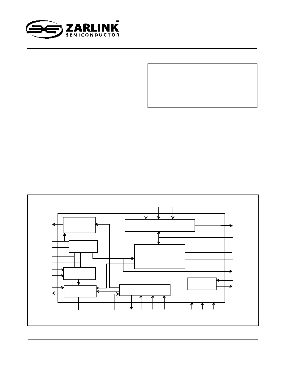
Figure 1 - Functional Block Diagram
TD
RING
Tip Drive
Controller
Audio Gain & Network
Balance Circuit
2 W to 4 W
Conversion & Line
Impedance
Relay
Driver
Line Sense
Over-Current
Protection Circuit
Ring Drive
Controller
Loop Supervision
TIP
TF
RF
C3A
C3B
RV
RD
VR
Z3
Z2
Z1
RLYC
RLYD
VEE
GND
VDD
C2B
C2A
C1
SHK
VREF
IC
X3
X2
X1
VX

MT91600
Data Sheet
2
Zarlink Semiconductor Inc.
Change Summary
Figure 2 - Pin Connections
Page
Item
Change
10
Figure 5
Updated Application Diagram
Pin Description
Pin #
Name
Description
1
VDD
Positive supply rail, +5 V.
2
TD
Tip Drive (Output). Controls the Tip transistor.
3
TF
Tip Feed. Connects to the Tip transistor and to the TIP lead via the Tip feed resistor.
4
TIP
Tip. Connects to the TIP lead of the telephone line.
5
RING
Ring. Connects to the RING lead of the telephone line.
6
VREF
Reference Voltage (Input). This pin is used to set the subscribers loop constant
current. Changing the input voltage sets the current to any desired value within the
working limits. VREF is related to VLC.
7
IC
Internal Connection (Input). This pin must be connected to GND for normal operation.
8
RF
Ring Feed. Connects to the RING lead via the Ring feed resistor.
9
RV
Ring Voltage and Audio Feed. Connects directly to the Ring drive transistor and also to
Ring Feed via a relay.
10
RD
Ring Drive (Output). Controls the Ring transistor.
11
C3A
A filter capacitor for over-current protection is connected between this pin and GND.
12
C3B
A filter capacitor for over-current protection is connected between this pin and GND.
13
C2B
A capacitor for loop current stability is connected between this pin and C2A.
14
C2A
A capacitor for loop current stability is connected between this pin and C2B.
15
Z1
Line Impedance Node 1. A resistor of scaled value "k" is connected between Z1 and
Z2. This connection can not be left open circuit.
Z3
X3
VREF
RLYD
VEE
RF
GND
Z2
IC
RING
TIP
RV
1
2
3
4
5
6
7
8
9
10
11
12
13
14
28
27
26
25
24
23
22
21
20
19
18
17
16
15
TF
VDD
TD
RD
C3A
C3B
C2B
C2A
RLYC
SHK
C1
X2
VR
VX
X1
Z1

MT91600
Data Sheet
3
Zarlink Semiconductor Inc.
Functional Description
The MT91600 is the analog SLIC for use in a 4 Wire switched system. The SLIC performs all of the normal interface
functions between the CODEC or switching system and the analog telephone line such as 2 W to 4 W conversion,
constant current feed, ringing and ring trip detection, current limiting, switch hook indication and line and network
balance impedance setting using minimal external components.
Refer to Figure 5 for MT91600 components designation.
2 Wire to 4 Wire Conversion
The hybrid performs 2 wire to 4 wire conversion by taking the 4 wire signal from an analog switch or voice CODEC,
a.c. coupled to VRIN, and converting it to a 2 wire differential signal at tip and ring. The 2 wire signal applied to tip
and ring by the telephone is converted to a 4 wire signal and should be a.c. coupled to Vx which is the output from
the SLIC to the analog switch or voice CODEC input.
Gain Control
It is possible to set the Transmit and Receive gains by the selection of the appropriate external components.
The gains can be calculated by the formulae:
2W to 4W gain:
Gain 2 - 4 = 20*Log [ R13 / R12]
4W to 2W gain:
Gain 4 - 2 = 20*Log [0.891 * (R14 / R15)]
16
Z2
Line Impedance Node 2. This is the common connection node between Z1 and Z3.
17
Z3
Line Impedance Node 3. A network either resistive or complex of scaled value "k" is
connected between Z3 and Z2. This connection can not be left open circuit.
18
X1
Gain Node 1. This is the common node between Z3 and VX where resistors are
connected to set the 2 W to 4 W gain.
19
VX
Transmit Audio (Output). This is the 4 W analog signal to the SLIC.
20
X3
Gain Node 3. This is the common node between VR and the audio input from the
CODEC or switching network where resistors are fitted to sets the 4 W to 2 W gain
21
VR
Receive Audio (Input). This is the 4 W analog signal to the SLIC.
22
X2
Gain Node 2. Networks, either resistive or complex, are connected between this node,
VR and GND to set the Network Balance Impedance for the SLIC.
23
C1
A filter capacitor for ring trip is connected between this pin and GND.
24
SHK
Switch Hook (Output). This pin indicates the line state of the subscribers telephone.
The output can also be used for dial pulse monitoring. SHK is high in off-hook state.
25
RLYC
Relay Control (Input). An active high on this pin will switch RLYD low.
26
RLYD
Inverted Output of RLYC. It is used to drive the bipolar transistor that drives the relay
(see Figure 5.)
27
GND
Ground. Return path for +5 V and -5 V. This should also be connected back to the
return path for the loop battery, LGND and relay drive ground RLYGND.
28
VEE
Negative supply rail, -5 V.
Pin Description (continued)
Pin #
Name
Description

MT91600
Data Sheet
4
Zarlink Semiconductor Inc.
Impedance Programming
The MT91600 allows the designer to set the device's impedance across TIP and RING, (Z
TR
), and network balance
impedance, (Z
NB
), separately with external low cost components.
For a resistive load, the impedance (Z
TR
) is set by R11 and R18. For a complex load, the impedance (Z
TR
) is set by
R11, R18, R19 & C8 (see Figure 5.)
The network balance, (Z
NB
), is set by R16, R17 & C3 (see Figure 5.)
The network balance impedance should be calculated once the 2W - 4W gain has been set.
Line Impedance
For optimum performance, the characteristic impedance of the line, (Z
o
), and the device's impedance across TIP
and RING, (Z
TR
), should match. Therefore:
Z
o
= Z
TR
The relationship between Z
o
and the components that set Z
TR
is given by the formula:
Z
o
/ ( R1+R2) = kZ
o
/ R11
where kZ
o
= Z
LZ
Z
LZ
= R18, for a resistive load.
Z
LZ
= [R18 + (R19 // C8)], for a complex load.
The value of k can be set by the designer to be any value between 20 and 250. Three rules to ensure the correct
operation of the circuit:
(A) R18 + R19 > 50k
(B) R1 = R2.
(C) R11 > =50k
It is advisable to place these components as close as possible to the SLIC.
Network Balance Impedance
The network balance impedance, (Z
NB
), will set the transhybrid loss performance for the circuit. The balance of the
circuit is independent of the 4 - 2 Wire gain but is a function of the 2 - 4 Wire gain.
The method of setting the values for R16 and R17 is given by the formula:
R17 = [1.782 * Z
o
/ ( Z
o
+Z
NB
) * ( R13 / R12 )]
R17 + R16
[1 + R13 / R12]
where Z
NB
is the network balance impedance of the SLIC and Z
o
is the line impedance.
(R16 + R17) >= 50k
It is advisable to place these components as close as possible to the SLIC.

MT91600
Data Sheet
5
Zarlink Semiconductor Inc.
Loop Supervision & Dial Pulse Detection
The Loop Supervision circuit monitors the state of the phone line and when the phone goes "Off Hook" the SHK pin
goes high to indicate this state. This pin reverts to a low state when the phone goes back "On Hook" or if the loop
resistance is too high for the circuit to continue to support a constant current.
The SHK output can also be monitored for dialing information when used in a dial pulse system.
Constant Current Control
The SLIC employs a feedback circuit to supply a constant feed current to the line. This is done by sensing the sum
of the voltages across the feed resistors, R1 and R2, and comparing it to the input reference voltage, Vref, that
determines the constant current feed current.
The MT91600's programmable current range is between 18 mA to 32 mA.
Line Drivers & Overcurrent Protection
The Line Drivers control the external Battery Feed circuit which provide power to the line and allows bi-directional
audio transmission.
The loop supervision circuitry provides bias to the line drivers to feed a constant current while the over-current
protection circuitry prevents the ring driver from causing the ring transistor to overload.
The line impedance presented by the Line Driver circuitry is determined by the external network, which may be
purely resistive or complex, allowing the circuit to be configured for use in any application. The impedance can also
be fixed to one value and modified to look like a different value by reflecting an impedance through the SLIC from
an intelligent CODEC or DSP module.
There is long term protection on the RING output against accidental short circuits that may be applied either across
TIP/RING to GND or RING to GND. This high current will be sensed and limited to a value that will protect the
circuit.
In situations where an accidental short circuit occurs either across TIP/RING to GND or RING to GND, an
excessive amount of current will flow through the ring drive transistor, Q3. Although the MT91600 will sense this
high current and limit it, if the power rating of Q3 is not high enough, it may suffer permanent damage. In this case,
a power sharing resistor, R23, can be inserted (see Figure 5) to dissipate some of the power. Capacitor C13 is
inserted to provide an a.c. ground point. The criteria for selecting a value for the power sharing resistor R23 can be
found in the application section of this data sheet.
Ringing and Ring Trip Detection
Ringing is applied to the line by disconnecting pin 8, RF, from pin 9, RV, and connecting it to a ringing source which
is battery backed. This may be done by use of an electro-mechanical relay. The SLIC is capable of detecting an Off
Hook condition during ringing by filtering out the large A.C. component by use of the external components
connected to pin 23. This filter allows an Off Hook condition to be monitored at SHK, pin 24.
When using DTMF signalling only i.e., pulse dialling is not used, the capacitor, C7, can be permanently connected
to ground and does not require to be switched out during dialling.
Power up Sequence
The circuit should be powered up in the following order: AGND, VEE, VDD, V
BAT.