 | –≠–ª–µ–∫—Ç—Ä–æ–Ω–Ω—ã–π –∫–æ–º–ø–æ–Ω–µ–Ω—Ç: SL1935 | –°–∫–∞—á–∞—Ç—å:  PDF PDF  ZIP ZIP |
Features
∑
∑
∑
∑
∑
∑
∑
∑
∑
∑
∑
Single chip synthesised tuner solution for quadrature
down conversion, L-band to Zero IF.
DVB compliant, operating dynamic range -70 to
-20dBm.
Compatible with DSS and DVB variable symbol rate
applications.
Selectable baseband path, programmable through
I
2
C bus.
Excellent quadrature balance up to 30MHz
baseband
Excellent immunity to spurious second harmonic
(RF and LO) mixing effects.
Low oscillator phase noise and reradiation.
High output referred linearity for low distortion and
multi channel application.
Integral fast mode compliant I
2
C bus controlled PLL
frequency synthesiser, designed for high comparison
frequencies and low phase noise performance.
Buffered crystal output for clocking QPSK
demodulator.
ESD protection (Normal ESD handling procedures
should be observed).
Applications
∑
∑
Satellite receiver systems.
Data communications systems.
Figure 1.
Pin connections
36
1
18
19
XTALCAP
XTAL
SDA
SCL
BUFREF
VCCD
VCC
RF
RFB
VCC
IFIA
IFIB
VCC
OFIA
OFIB
VEE
IOUT
ADD
PUMP
DRIVE
PORT P0
VEE
TANKS
TANKSB
VEE
TANKV
TANKVB
VEE
IFQA
IFQB
VCC
OFQA
OFQB
VEE
QOUT
AGCCONT
Description
The SL1935 is a complete single chip
bus controlled
Zero IF tuner and operates from 950 to 2150MHz. It
includes an on-board low phase noise PLL frequency
synthesiser and low noise LNA/AGC. The SL1935 is
intended primarily for application in digital satellite Network
Interface Modules and performs the complete tuner
function.
The device contains all elements necessary, with the
exception of local oscillator tuning network and crystal
reference, to produce a high performance I(n-phase) &
Q(uadrature) downconversion tuner function. Due to the
high signal handling design the device does not require
any front end tracking filters.
The SL1935 includes selectable baseband signal paths,
allowing application with two externally definable filter
bandwidths, facilitating application in variable symbol
rate and simulcast systems. The SL1935 is optimised to
interface with the VP310 (ADC/QPSK/FEC) Satellite
Channel Decoder, available from Zarlink Semiconductor
and offers a full front end solution.
I
2
C
SL1935
Single Chip Synthesized Zero IF Tuner
April 2004
Ordering Information
SL1935
D/KG/NP1P (Tubes) 36 pin SSOP
SL1935
D/KG/NP1Q (Tape and Reel) 36 pin SSOP
1
Zarlink Semiconductor Inc.
Zarlink, ZL and the Zarlink Semiconductor logo are trademarks of Zarlink Semiconductor Inc.
Copyright 2003 - 2004, Zarlink Semiconductor Inc. All Rights Reserved.
2
SL1935
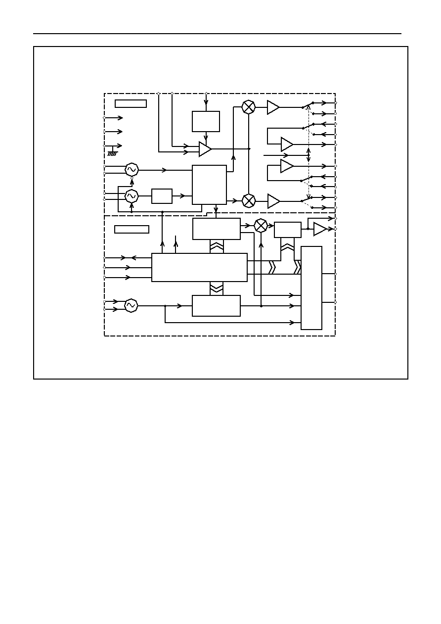
Figure 2.
Block diagram
Frequency
Agile
Phase
Splitter
AGC
Sender
Divide
by 2
15 bit
Programmab le
Divider
I
2
C Bus Interface
Charge
Pump
Reference
Divider
VCC
7,10,13,24
VCCD
VEE
16,21,27,30,33
AGCCONT
RF
8
RFB
9
6
TANKS 3 2
TANKSB 31
TANKV 29
TANKVB 28
SDA 3
SCL 4
ADD 18
XTAL 2
XTALCAP 1
5 BUFREF
34 POR T P0
35 DRIVE
36 PUMP
15 OFIB
14 OFIA
12 IFIB
11 IFIA
17 IOUT
20 QOUT
26 IFQA
25 IFQB
23 OFQA
22 OFQB
Fpd/2
Fcomp
Fpd
REF
OSC
VCOV
VCOS
VS
BS
RF section
PLL section
PLL Section
BS
RF Section
90deg
0deg
19

3
SL1935
Table 1.
Quick Reference Data
Functional Description
General
The SL1935 is a complete wideband direct conversion
tuner incorporating an on board frequency synthesiser
and LNA/AGC, optimised for application in digital satellite
receiver systems. The device offers a highly integrated
solution to a satellite tuner function, incorporating an I
2
C
bus interface controller, a low phase noise PLL frequency
synthesiser and all tuner analogue functionality. The
analogue blocks include the reference oscillator,
consisting of two independent oscillators, a phase splitter,
RF preamplifier with AGC facility, channel mixers and
baseband amplifiers incorporating two selectable
baseband paths, allowing for two externally definable
bandwidths. In this application two varactor tuned tanks,
a reference crystal and baseband filtering components
are required to complete the tuner system.
A buffered crystal frequency output is available to clock
the QPSK demodulator and powers up in the active
state.
The I
2
C bus interface controls the frequency synthesiser,
the local oscillator, the baseband path selection, the
buffered reference frequency output and an external
switching port.
Figure 2 shows the device block diagram and pin
allocations are shown in Figure 1.
Quadrature Downconverter Section
In normal application the tuner IF frequency of typically
950 to 2150MHz is fed direct to the SL1935 RF input
through an appropriate impedance match (Fig.16) and
LNB switching. The input stage is optimised for both NF
and signal handling.
The signal handling of the front end is designed to offer
immunity to input composite overload without the
requirement of a tracking filter. RF input impedance is
shown in Fig.3.
The RF input amplifier feeds an AGC stage and provides
system gain control. The system AGC gain range will
guarantee an operating dynamic range of -70 to -20dBm.
The AGC is controlled by the AGC sender and is optimised
for S/N and S/I performance across the full dynamic
range. Details of the AGC characteristics, variations in
IIP3, IIP2, P1dB and NF are illustrated in Figs.4, 5, 6, 7,
and 8 respectively.
The required I and Q local oscillator frequencies for
quadrature downconversion are generated by the on-
board reference oscillators designated `VCOS' and
`VCOV'. VCOS operates nominally from 1900 to 3000MHz
and is then divided by two to provide 950 to 1500MHz.
VCOV operates nominally from 1400 to 2200MHz. Only
the oscillator selected via bit VS in the I
2
C data
transmission is powered.
Characteristic
Value
Units
Operating range
Input dynamic range
VSWR with input match
Input NF
@ -70dBm operating sensitivity
@ -60dBm operating sensitivity
IPIP3 @ -20dBm operating sensitivity
IPIP2@ -20dBm operating sensitivity
IPP1dB@ -20dBm operating sensitivity
Baseband output limit voltage
Gain match up to 22MHz
Phase match up to 22MHz
Gain flatness up to 30MHz
Local oscillator phase noise
SSB at 10kHz offset
In band LO reradiation from RF input
LO second harmonic interference level at input level of
-20dBm per carrier
LNA second harmonic interference level at input level
of -25dBm per carrier
PLL maximum comparison frequency
PLL phase noise at phase detector
950 to 2150
-75 to -15
10
10
15
+5
+20
-5
2.0
0.2
0.7
1
-80
<-70
-55
-35
4
-152
MHz
dBm
dB
dB
dB
dBm
dBm
dBm
V
dB
deg
dB
dBc/Hz
dBm
dBc
dBc
MHz
dBc/Hz
Note:
6dB interstage filter loss assumed in external base band paths.
dBm assumes 75
characteristic impedance.
`
`

4
SL1935
Quadrature Downconverter
Section - continued
The oscillators share a common varactor line drive and
both require an external varactor tuned resonator
optimised for low phase noise performance. The
recommended application circuit for the local oscillators
is detailed in Fig.9 and the typical phase noise
performance is detailed in Fig.10. The local oscillator
frequency is coupled internally to the PLL frequency
synthesiser programmable divider input.
The mixer outputs are coupled to the baseband buffer
amplifiers, providing for one of two selectable baseband
outputs in each channel. The required output is selected
by bit BS in the I
2
C bus transmission (Table 6). These
outputs are fed off chip via ports `OPIA' and `OPIB'
(`OPQA' and `OPQB'), then back on chip through ports
`IPIA' and `IPIB' (`IPQA' and `IPQB'), allowing for the
insertion of two independent user definable filter
bandwidths. Each output provides a low impedance
drive (Fig.11) and each input provides a high impedance
load . An example filter for 30MS/s is detailed in Fig.13.
Both path gains are nominally equal. NB 6dB insertion
loss is assumed in each channel, however a different pot
down ratio may be applied.
Each baseband path is then multiplexed to the final
baseband amplifier stage, providing further gain and a
low impedance output drive. The nominal output load
test condition is detailed in Fig.14.
PLL Frequency Synthesiser Section
The PLL frequency synthesiser section contains all the
elements necessary, with the exception of a reference
frequency source and a loop filter to control the selected
oscillator to produce a complete PLL frequency
synthesised source. The device, produced using high
speed logic, allows for operation with a high comparison
frequency and enables the generation of a loop with
excellent phase noise performance.
The LO signal from the selected oscillator drives from the
phase splitter into an internal preamplifier, providing gain
and reverse isolation from the divider signals. The output
of the preamplifier interfaces directly with the 15-bit fully
programmable divider. The programmable divider has
MN+A architecture, the dual modulus prescaler is 16/17,
the A counter is 4-bits and the M counter is 11-bits.
The output of the programmable divider is fed to the
phase comparator and compared in both phase and
frequency domains to the comparison frequency. This
frequency is derived from either the on board crystal
controlled oscillator or from an external reference source.
In both cases the reference frequency is divided down to
the comparison frequency by the reference divider,
programmable into 1 of 29 ratios and detailed in Table 3.
The typical application for the crystal oscillator is shown
in Fig.15.
The output of the phase detector feeds a charge pump
and a loop amplifier. When used with an external loop
filter and a high voltage transistor it integrates the current
pulses into the varactor line voltage used to control the
selected oscillator.
The programmable divider output Fpd divided by two
and the reference divider output Fcomp are switched to
port P0 by programming the device into test mode. Test
modes are detailed in Table 4.
The crystal reference frequency can be switched to the
BUFREF output by bit RE as detailed in Table 7.
Programming
The SL1935 is controlled by an I
2
C data bus and is
compatible with both standard and fast mode formats.
Data and Clock are fed on the SDA and SCL lines
respectively as defined by the I
2
C bus format. The
device can either accept data (write mode) or send data
(read mode). The LSB of the address byte (R/W) sets the
device into write mode if it is low and read mode if it is
high. Tables 9a and 9b detail the format of the data. The
SL1935 may be programmed to respond to several
addresses and enables the use of more than one device
in an I
2
C bus system. Table 9c details the how the
address is selected by applying a voltage to the `ADD'
input. When the device receives a valid address byte, it
pulls the SDA line low during the acknowledge period
and during following acknowledge periods after further
data bytes are received. When the device is
programmed into read mode, the controller accepting
the data must pull the SDA line low during all status byte
acknowledge periods to read another status byte. If the
controller fails to pull the SDA line low during this period,
the device generates an internal `STOP' condition which
inhibits further reading.
Write mode
Bytes 2 and 3 contain frequency information bits 2
14
to 2
0
inclusive (Table 9). Byte 4 controls the synthesiser
reference divider ratio (Table 3) and the charge pump
setting (Table 5). Byte 5 controls test modes (Table 4),
baseband filter path select BS (Table 6), local oscillator
select VS (Table 8), buffered crystal reference output
select RE (Table 7) and the output port P0.
After reception and acknowledgment of a correct
address (byte 1), the first bit of the following byte
determines whether the byte is interpreted as byte 2 or
4, a logic `0' indicates byte 2 and a logic `1' indicates byte
4. Having interpreted this byte as either byte 2 or 4, the
following byte will be interpreted as byte 3 or 5
respectively. After receiving two complete data bytes,
additional data bytes may be entered and byte
interpretation follows the same procedure without re-
addressing the device. The procedure continues until a
`STOP'
condition is received.

5
SL1935
The STOP condition can be generated after any data
byte, if however it occurs during a byte transmission, the
previous byte data is retained. To facilitate smooth fine
tuning, the frequency data bytes are only accepted by
the device after all 15 bits of frequency data have been
received, or after the generation of a STOP condition.
Read mode
When the device is in read mode, the status byte read
from the device takes the form shown in Table 9b.
Synthesiser programmable divider
Reference programmable divider
Baseband filter path select
Local oscillator select
Charge pump current
Test mode
General purpose port, P0
Buffered crystal reference output,
BUFREF
Programmable features
Function as described above
Function as described above.
Function as described above.
Function as described above.
The charge pump current can be programmed by bits C1 & C0 (Table 5).
The test modes are defined by bits T2 - T0 as described in Table 4.
The general purpose port can be programmed by bit P0;
Logic `1' = on
Logic `0' = off (high impedance)
The buffered crystal reference frequency can be switched to the BUFREF
output by bit RE as described in Table 7. The BUFREF output defaults to
the `ON' condition at device power up.
Bit 1 (POR) is the power-on reset indicator, and this is set
to a logic `1' if the Vccd supply to the device has dropped
below 3V (at 25oC), e.g. when the device is initially turned
ON. The POR is reset to `0' when the read sequence is
terminated by a STOP command. When POR is set high
this indicates that the programmed information may
have been corrupted and the device reset to the power
up condition.
Bit 2 (FL) indicates whether the synthesiser is phase
locked, a logic `1' is present if the device is locked, and
a logic `0' if the device is unlocked.
The typical key performance data at Vcc = 5V and +25oC
ambient
are detailed in Table
1.
Function
Table 2. Programmable Features
R4
0
0
0
0
0
0
0
0
0
0
0
0
0
0
0
0
1
1
1
1
1
1
1
1
1
1
1
1
1
1
1
1
R3
0
0
0
0
0
0
0
0
1
1
1
1
1
1
1
1
0
0
0
0
0
0
0
0
1
1
1
1
1
1
1
1
R2
0
0
0
0
1
1
1
1
0
0
0
0
1
1
1
1
0
0
0
0
1
1
1
1
0
0
0
0
1
1
1
1
R1
0
0
1
1
0
0
1
1
0
0
1
1
0
0
1
1
0
0
1
1
0
0
1
1
0
0
1
1
0
0
1
1
R0
0
1
0
1
0
1
0
1
0
1
0
1
0
1
0
1
0
1
0
1
0
1
0
1
0
1
0
1
0
1
0
1
Ratio
2
4
8
16
32
64
128
256
Illegal state
5
10
20
40
80
160
320
Illegal state
6
12
24
48
96
192
384
Illegal state
7
14
28
56
112
224
448
Table 3. Reference division ratios