Obsolescence Notice
This product is obsolete.
This information is available for your
convenience only.
For more information on
Zarlink's obsolete products and
replacement product lists, please visit
http://products.zarlink.com/obsolete_products/

SL3145
1.6GHz NPN TRANSISTOR ARRAYS
The SL3145 is a monolithic array of five high frequency low
current NPN transistors. The SL3145 consists of 3 isolated
transistors and a differential pair in a 14 lead SO package The
transistors exhibit typical f
TS
of 1.6GHz and wideband noise
figures of 3.0dB The device is pin compatible with the CA3046.
FEATURES
s
f
T
Typically 1.6GHz
s
Wideband Noise Figure 3.0dB
s
V
BE
Matching Better Than 5mV
APPLICATIONS
s
Wide Band Amplifiers
s
PCM Regenerators
s
High Speed Interface Circuits
s
High Performance Instrumentation Amplifiers
s
High Speed Modems
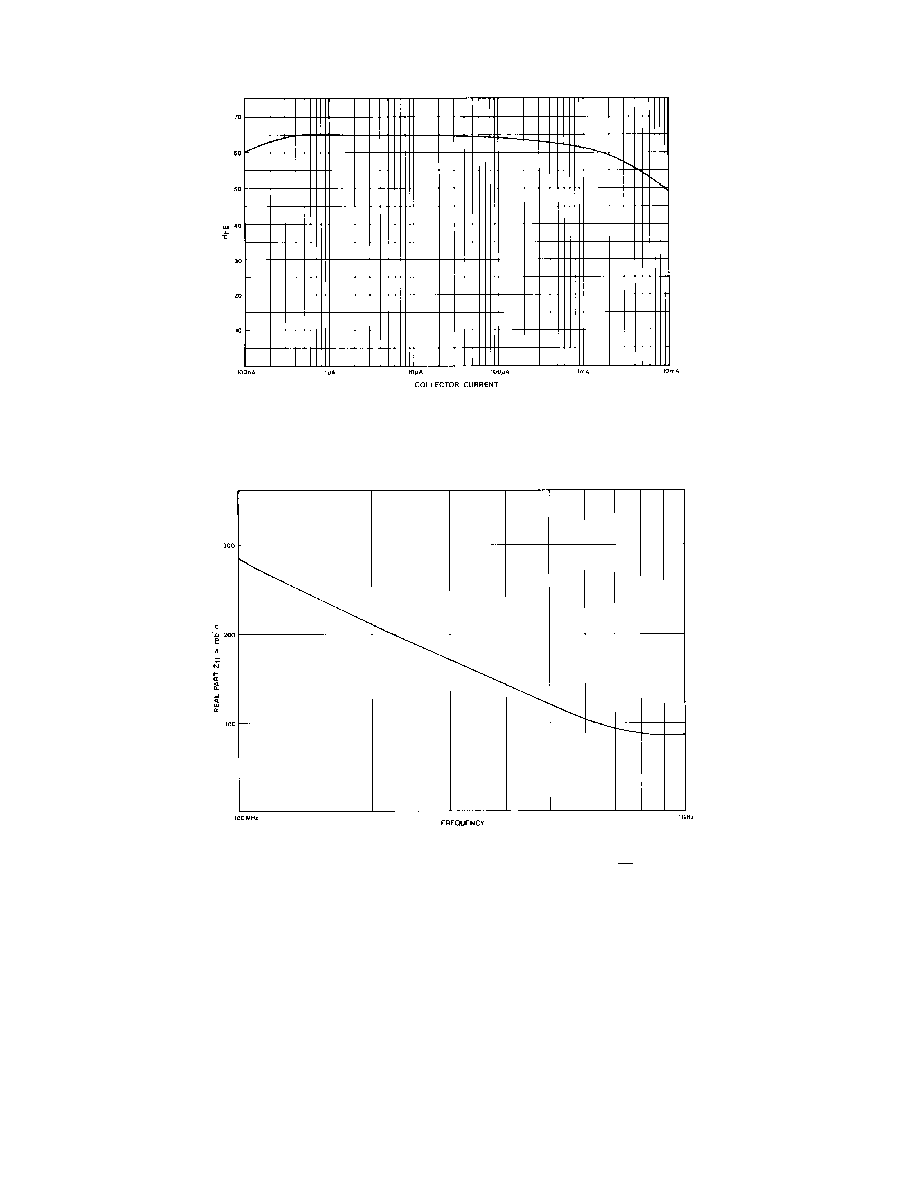
Fig.1 Pin connections SL3145
MP14
Fig.2 Transition frequency (f
T
) v. collector current (V
CB
= 2V, f=200MHz)
DS3627 - 1.3
ORDERING INFORMATION
SL3145 C MP
ADVANCE INFORMATION
SL3145
30
18
55
20
0.74
0.26
0.1
0.95
0.45
0.35
0.2
0.2
2.0
-1.6
100
0.3
0.6
100
0.4
0.4
0.8
1.6
3.0
1
20
15
20
10
0.64
40
BV
CBO
LV
CEO
BV
CIO
BV
BIO
V
BE
V
CE
(SAT)
I
EBO
V
BE
(SAT)
V
BE
V
BE
I
B
I
B
V
BE
T
V
BE
T
H
FE
I
CBO
I
CIO
I
BIO
C
EB
C
CB
C
CI
f
T
NF
ELECTRICAL CHARACTERISTICS
These characteristics are guaranteed over the following test conditions (unless otherwise stated)
T
amb
= 22
∞
C
±
2
∞
C
0.84
0.5
1
5
5
3
2
Value
Units
Conditions
Min.
Typ.
Max.
Symbol
Static characteristic
Collector base breakdown
Collector emitter breakdown
Collector substrate breakdown (isolation)
Base to isolation breakdown
Base emitter voltage
Collector emitter saturation voltage
Emitter base leakage current
Base emitter saturation voltage
Base emitter voltage difference,
all transistors expect TR1, TR2
Base emitter voltage difference
TR1, TR2
Input offset current
(except for TR1, TR2)
Input offset current TR1, TR2
Temperature coefficient of
V
BE
Temperature coefficiient of V
BE
Static forward current ratio
Collector base leakage
Collector isolation leakage
Base isolation leakage
Emitter base capacitance
Collector base capacitance
SL3145
Collector isolation capacitance
Dynamic characteristics
Transition frequency
SL3145
Wideband noise figure
Knee of 1/f noise curve
V
V
V
V
V
V
µ
A
V
mV
mV
µ
A
µ
A
µ
V/
∞
C
mV/
∞
C
nA
nA
nA
pF
pF
pF
GHz
dB
KHz
I
C
= 10
µ
A, I
E
= 0
I
C
= 1mA, I
B
= 0
I
C
= 10
µ
A, I
R
= I
E
= 0
I
B
= 10
µ
A, I
C
= I
E
= 0
V
CE
= 6V, I
C
= 1mA
I
C
= 10mA, I
B
= 1mA
V
EB
= 4V
I
C
= 10mA, I
B
= 1mA
V
CE
= 6V, I
C
= 1mA
V
CE
= 6V, I
C
= 1mA
V
CE
= 6V, I
C
= 1mA
V
CE
= 6V, I
C
= 1mA
V
CE
= 6V, I
C
= 1mA
V
CE
= 6V, I
C
= 1mA
V
CB
= 16V
V
CI
= 20V
V
BI
= 5V
V
EB
= 0V
V
CB
= 0V
V
CI
= 0V
V
CE
= 6V, I
C
= 5mA
V
CE
= 2V, R
S
= 1k
I
C
= 100
µ
A, f = 60MHz
V
CE
= 6V, R
S
= 200
I
C
= 2mA
Characteristic
ABSOLUTE MAXIMUM RATINGS
The absolute maximum ratings are limiting values above
which operating life may be shortened or specified parameters
may be degraded.
All electrical ratings apply to individual transistors. Thermal
ratings apply to the total package.
The isolation pin (substrate) must be connected to the most
negative voltage applied to the package to maintain electrical
isolation.
V
CB
= 20 volt
V
EB
= 4.0 volt
V
CE
= 15 volt
V
CI
= 20 volt
I
C
= 20 mA
Maximum individual transistor dissipation 200 mWatt
Storage temperature -55
∞
C to 150
∞
C
Max junction temperature 150
∞
C
Package thermal resistance (
∞
C/watt):-
Package Type
MP14
Chip to case
45
∞
C/W
Chip to ambient
123
∞
C/W
NOTE:
If all the power is being dissipated in one transistor, these
thermal resistance figures should be increased by 100
∞
C/watt

SL3145
Fig.3 Transition frequency (f
T
) v. collector base voltage
(I
C
= 5mA, Frequency = 200MHz)
Fig.4 Variation of transition frequency (f
T
) with temperature