
Obsolescence Notice
This product is obsolete.
This information is available for your
convenience only.
For more information on
Zarlink's obsolete products and
replacement product lists, please visit
http://products.zarlink.com/obsolete_products/
1
ZIF600
The ZIF600 synthesiser is for channel selection in 4FSK
pagers. A reference frequency is generated by an on-chip
crystal oscillator with an AFC external trimming varacator
controlled by a DAC.
The ZIF600 digital demodulator uses DSP techniques to
optimise the data extraction in the presence of noise and also
generates an AFC output to adjust the crystal frequency.
Separate power controls allow the system current
consumption to be minimised. All functions are controlled by a
serial bus with a simple programming format and with four
control pins which are used to control the power up and power
down functions of the blocks to allow sequenced wake up and
optimised power consumption.
FEATURES
s
Low Voltage Operation, 2.7 to 3.3V
s
On-chip Reference Oscillator
s
Channel Select Synthesiser
s
Direct VCO input at up to 330MHz
s
6400 Baud Digital 4FSK Demodulator
s
Serial Control Bus
s
Very Low Power Consumption
s
Small QSOP24 Package
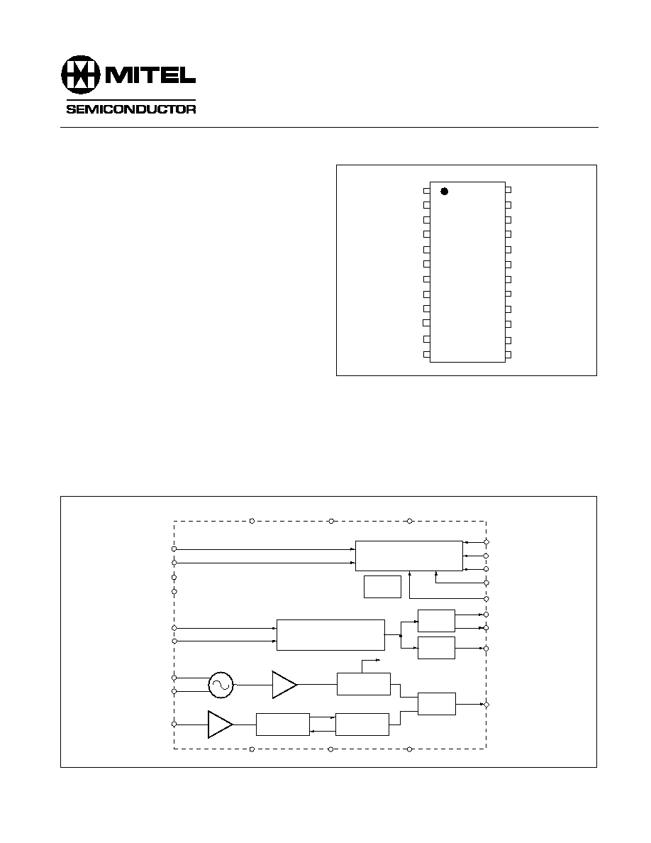
Fig.1 Pin connections - top view
QP24
APPLICATIONS
s
Pagers - including small form factor designs such as
credit card pagers, watch pagers and PCMCIA
applications
s
Low data rate receivers - security/remote control
ABSOLUTE MAXIMUM RATINGS
To be defined.
Fig.2 ZIF600 block diagram
ZIF600
1
2
3
4
5
6
7
8
9
10
11
12
24
23
22
21
20
19
18
17
16
15
14
13
RXQ
RXI
SRF
DATA0
DATA1
VSSD
VDDD
VREF
RBIAS
PDOUT
PLLC
DACOUT
DSC2
DSC1
DATA
LE
CLOCK
VSSA
VCOFIN
VDDA
REFOSCB
TSS
REFOSC
VSSI
RXI
RXQ
PHASE
DETECTOR
CONTROL LOGIC &
POWER MANAGEMENT
DSC2
DATA1
REFOSC
REFOSB
VCOFIN
DATA
CLOCK
VDDA
VDDD
TSS
VSSA
PLLC
SRF
VSSI
BIASES
VREF
RBIAS
DATA
SLICER
AFC
(DAC)
DIGITAL DEMODULATOR
REFERENCE
DIVIDER
M AND A
DIVIDERS
LE
DSC1
DACOUT
PDOUT
DATA0
TWO MODULUS
PRESCALER
VSSD
LIMI
LIMQ
Demod. Clock
ZIF600
Pager Synthesiser and 4FSK Demodulator
DS4771 - 1.2 October 1997

2
ZIF600
TARGET ELECTRICAL CHARACTERISTICS
These characteristics are guaranteed over the following conditions (unless otherwise stated):
VDDD, VDDA = 2.7 TO 3.3V, VDD1 = 0.95V to 1.6V (connected to REFOSCB via ext. resistor) and T
amb
= --20 to + 70
�
C
Characteristic
Min.
Typ.
Max.
Units
Conditions
Supply current at VDDD,VDDA = 3V
-
1
-
mA
Synthesiser locked and
demodulator active. VDD1
Supply current at VDD1 = 1.4V
-
350
-
�
A
connected to REFOSCB
via external resistor.
VREF bias voltage input range
1.15
1.25
1.31
V
Logic input HIGH, pins DATA, CLOCK,
VDD - 0.3
-
VDD + 0.3
V
LE, DSC1, DSC2, PLLC, SRF, RXI, RXQ
Logic input HIGH, pins DATA, CLOCK,
VSS - 0.3
-
VSS + 0.3
V
LE, DSC1, DSC2, PLLC, SRF, RXI, RXQ
Input capacitance (signal pins)
-
-
10
pF
Pin voltage: VSS to VDD
Input leakage (signal pins)
-
-
1
�
A
Pin voltage: VSS to VDD
Control bus CLOCK frequency
0
-
10
MHz
Synthesiser charge pump output
-
50
-
nA
Pin voltage:
leakage, pin PDOUT
VSS to VDD
Synthesiser charge pump output
160
200
240
�
A
Pin VDD/2
current, pin PDOUT
Charge pump output compliance
VSS + 0.4
-
VDD -- 0.4
V
Current within 10% of its
range, pin PDOUT
value at VDD/2
Main synthesiser input frequency on
50
-
330
MHz
VCOFIN
VCOFIN input level
300
-
1000
mV
pk - pk
Reference Frequency Crystal
-
12.8
-
MHz
Pins REFOSC and
14.4
REFOSCB
Logic output HIGH, pins DATA0,
VDD -- 0.3
-
VDD
V
Output current, IoH =
DATA1
100
�
A
Logic output LOW, pins DATA0,
VSS
-
VSS -- 0.3
V
Output current, IoL =
DATA1
100
�
A.
Trim DAC output voltage, pin DACOUT
0
-
2.375
V
Not tested Output current
100nA VREF = 1.25V
RXI, RXQ pull-up current
1.5
-
-
�
A
VDD -- 0.3V
RXI, RXQ pull-up current
-
-
40
�
A
VSS + 0.3V
Input leakage (signal) pins with
-
-
3
�
A
Pin voltage: VSS to VDD
pull-downs
pins include SRF, PLLC
DSC1, DSC2

3
ZIF600
FUNCTIONAL DESCRIPTION
The ZIF600 synthesiser is used to select the channel in
4FSK paging receivers and uses on-chip constant current
charge pumps to drive an external passive loop filter. Common
low cost reference crystals are used, at frequencies of 12.8 or
14.4MHz, and are divided to give the required 12.5, 20 or
25kHz channel spacings. The reference crystal oscillator uses
external trimming to meet system requirements and is controlled
by a DAC set by the digital demodulator.
The digital demodulator takes the limited I and Q signals
from the radio receiver and converts the 4-level FSK into 2 bit
data output on pins DATA0 and DATA1. An AFC output from
this demodulator is also included.
Functions are controlled by a serial bus with a simple
programming format and with four control pins to allow optimum
power up sequences which help minimise the system current
consumption.
DESCRIPTION OF FUNCTIONS
Pin No.
Pin Name
Pin Type
Description
1
RXQ
In
Receiver "Quadrature" output
2
RXI
In
Receiver "In Phase" output
3
SRF
In
Symbol Rate Filter
4
DATA0
Out
Data output to decoder
5
DATA1
Out
Data output to decoder
6
VSSD
G
Digital Ground
7
VDDD
P
2.7 to 3.3V Digital Power Supply
8
VREF
In
1.25 Volt Reference from ZIF100
9
RBIAS
In
Bias setting Resistor 120k
to VSSA max. parasitic capacitance = 5pF
10
PDOUT
Out
Charge pump output from synthesiser
11
PLLC
In
Synthesiser power down
12
DACOUT
Out
Trim DAC for crystal
13
VSS1
G
Ground (substrate)
14
REFOSC
I/O
Reference Oscillator
15
TSS
In
Test Scan Select, Normally logic 0
16
REFOSCB
I/O
Reference Oscillator. External resistor to VDD1
17
VDDA
P
2.7 to 3.3V Analog Power Supply
18
VCOFIN
In
VCO frequency input to synthesiser
19
VSSA
G
Analog Ground
20
CLOCK
In
Control Bus Clock
21
LE
In
Control Bus Latch Enable
22
DATA
In
Control Bus Data
23
DSC1
In
With DSC2 controls the operating mode of the demodulator
24
DSC2
In
With DSC1 controls the operating mode of the demodulator
Table 1. List of pins
REFERENCE DIVIDERS
The reference frequency generated by the oscillator on
pins REFOSC and REFOSCB is divided to give the comparison
frequency clock. See Fig. 3.
Ratio selection is five control bits RD1 (where LOW gives
�
8 mode), RD2 (where LOW gives
�
4 mode) and RD3 (where
LOW gives
�
2 mode) which can be set to give the 8 options
needed to get 10kHz, 12.5kHz, 20kHz or 25kHz from either a
12.8 or 14.4MHz crystal, as in Table 2. The additional control
bits RD4 and RD5 allow the option of further division to allow
for an off chip frequency multiplier. If both RD4 and RD5 are set
low then this division stage is bypassed. Other settings for RD4
and RD5 offer division by 2, 3 or 4. Table 3 shows the additional
division options available from RD4 and RD5.
Power down options are available for both the synthesiser
and demodulator, however the crystal oscillator and the
reference divider must be kept running to give a timing signal
to the demodulator whilst the demodulator is on.
Table 2 Reference divider ratios
Crystal
Comp.
Total
RD1
RD2
RD3
MHz
freq. kHz division
12.8
25
512
0
0
0
14.4
25
576
1
0
0
12.8
20
640
0
1
0
14.4
20
720
1
1
0
12.8
12.5
1024
0
0
1
14.4
12.5
1152
1
0
1
12.8
10
1280
0
1
1
14.4
10
1440
1
1
1
Table 3 Additional divider ratios
Additional division
RD4
RD5
Bypass
0
0
2
0
1
3
1
0
4
1
1
4
ZIF600
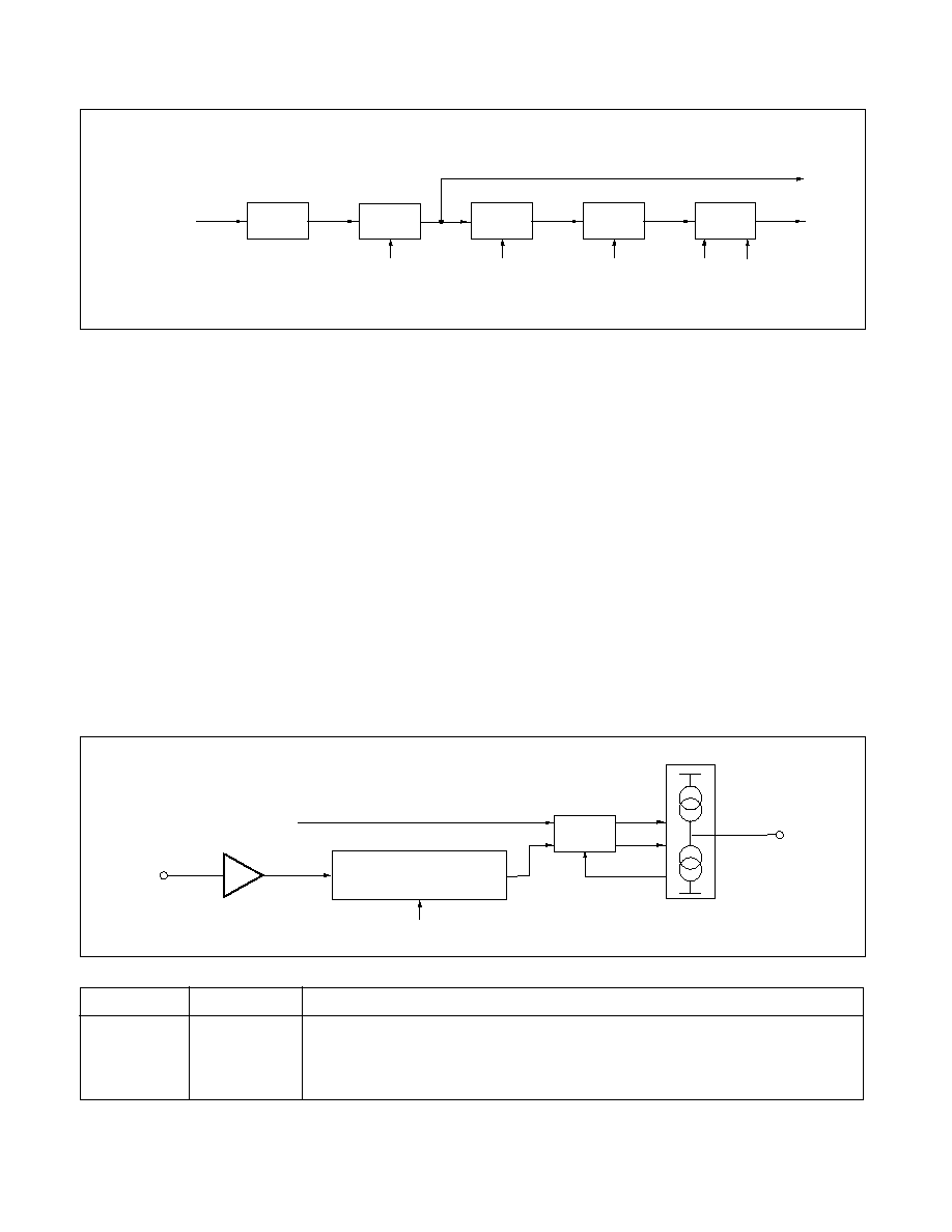
SYNTHESISER
The Synthesiser divides the VCOFIN frequency by the 16-
bit number FCH programmed from the serial bus and then the
phase detector compares the result with the comparison
frequency signal to generate correction pulses. The division
ratio range is 4,032 to 65,535.
An embedded two modulus prescaler is used to minimise
power consumption but its programming is arranged to be
transparent to the user.
By using a digital phase and frequency detector the loop will
pull in over an unlimited range and then by using a reset signal
fed back from the output current drivers any delays in the
output path do not give a dead band in the phase response.
The charge pump currents are set by internal biasing. The
current level fixed by the circuit has been selected to give
minimum loop disturbance from external interference, while
also not taking excessive current from the supply line. It is
expected that adequate high frequency decoupling will be
provided on the power supplies to eliminate any significant
noise.
Powering up the synthesiser requires that VREF, IBIAS
and PLLC have been turned on for an adequate time before the
synthesiser is required to be functioning.
As the demodulator takes its clock from the synthesiser
reference divider, the synthesiser reference oscillator and
divider circuits must be on and have settled before the
demodulator is turned on.
Setting the "DMO" bit in the control bus allows the main
parts of the synthesiser to be kept in a low power mode with
only the reference oscillator and reference divider operating,
when PLLC is high. This effectively allows the demodulator to
be used standalone with its required clock being provided by
the reference oscillator/divider.
Fig.4 Basic block diagram of synthesiser
"DMO" bit
PLLC
Synthesiser Mode
0
0
Synthesiser off
1
0
Synthesiser off
0
1
Synthesiser on
1
1
Reference oscillator and divider on, remainder of synthesiser circuitry off
Table 4. Synthesiser mode control
16 BIT DIVIDER
CHARGE
PUMP
PDOUT
PHASE
DETECTOR
FCH FROM BUS (16 bit)
RESET
COMPARISON FREQUENCY
(FROM REFERENCE DIVIDER)
VCOFIN
UP
DOWN
Fig.3 Reference divider configuration
�
8
�
8/9
RD1
�
4/5
RD2
�
2/4
RD3
�
1/2/3/4
RD4
RD5
CRYSTAL FREQUENCY
12�8 or 14�4 MHz
COMPARISON
FREQUENCY
200 kHz CLOCK TO DEMODULATOR
5
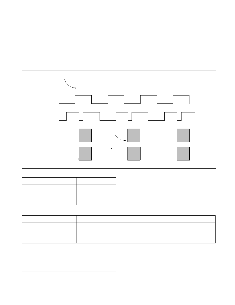
ZIF600
Fig.5 Response of DATA0 and DATA1 to a
�
4.8kHz I/Q input
DIGITAL DEMODULATOR
By using digital signal processing techniques it is possible
to get a very robust demodulator for 4-level FSK. The
demodulator produces a digital level depending on the received
frequency. A digital data slicer is used to encode the DATA0
and DATA1 signals. Extra functions are included to give an
AFC signal to the 8 bit Trim DAC for the crystal oscillator. The
DAC output will lag the incoming data, and will require some
external filtering to smooth DAC transitions (it is recommended
to connect a 10
�
F capacitor from DACOUT to Ground).
The demodulator receives "I" and "Q" signals from the
ZIF100. Fig.5 shows the DATA0 and DATA1 response to a 4
level I/Q input at
�
4.8kHz from te ZIF100. Table 5 maps the
input frequency represented by the I/Q demodulator inputs to
the DATA0 and DATA1 outputs.
The decoder will recover the symbol clock and sample the
DATA0 and DATA1 signals at the appropriate time. DATA1 will
have multiple edges during symbol transmissions.
In a typical application the ZIF600 receives real time control
from a decoder interface and provided the decoder with DATA0
and DATA1. Fig.6 illustrates the sequence of applied signals
from the Decoder in a typical application. Note that other
system ICs will require additional contol, and this may affect
the sequencing given.
DATA1
DATA0
Frequency Deviation
1
0
+4.8kHz
1
1
+1.6kHz
0
1
--1.6kHz
0
0
--4.8kHz
Table 5. Frequency map for DATA output pins
DSC2
DSC1
Demodulator Mode
0
0
Off, Hold Data Slicing and AFC loop values
1
0
On, Fast Tracking for Data Slicingand AFC loop
0
1
On, Slow Tracking for Data Slicingand AFC loop
1
1
Off, Hold applied to Data Slicing and AFC loop values
Table 6. Demodulator mode control
SRF
Symbol Rate
0
Symbol Rate Filter 1600sps
1
Symbol Rate Filter 3200sps
Table 7. Symbol rate filter control
I (4.8KHz)
Q
DATA0
DATA1
Symbol Transitions
Jitter
Typical Sampling Point
6
ZIF600
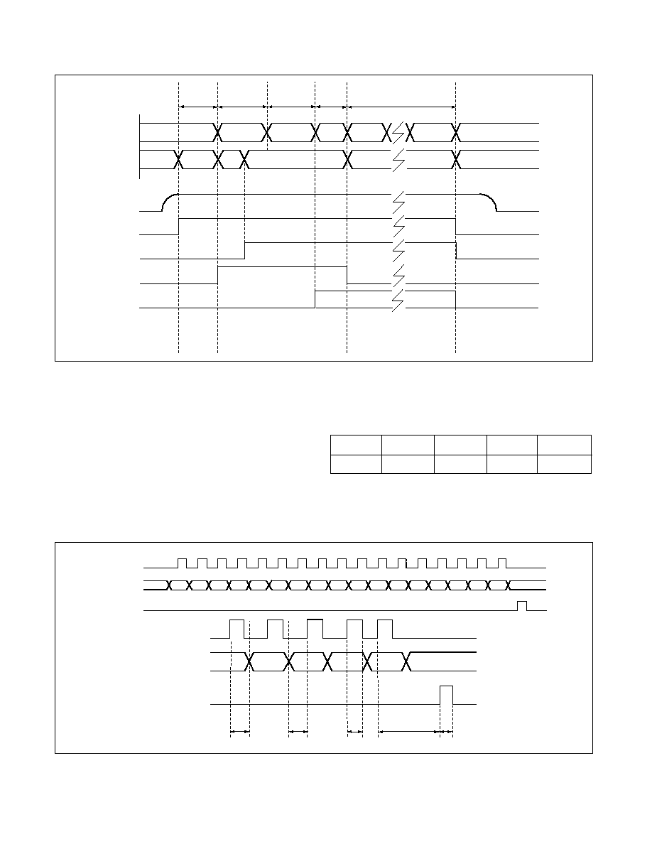
Fig.6 Control signal timing diagram for ZIF600 receiving data
Previous Signal
BS1
"A" -> Frame
Info
Sync 2
Block 0
Block 10
Next Signal
Off
Hold
Slow Track
Fast
Track
PLL Settle
Off
Signal
ZIF 600
Mode
VREF
PLLC
DSC1
DSC2
SRF
1.25v
0v
45mS
20mS
70mS
25mS
1�76 Sec.
VREF On
XTAL On
Synth. On
Demod. Off
Fast Track On
SRF=1600
Demod. On
Synth.On
Fast AFC On
Slow Track On
SRF=1600 or 3200
Demod. On
Synth.On
Slow AFC On
Hold Track
SRF=1600/3200
Demod. On
Synth.On
Hold AFC
SRF=1600
Demod. Off
Synth.On
Hold AFC
All
Off
All
Off
CONTROL BUS
The ZIF600 has its synthesiser and demodulator configured
by a three wire control bus (CLOCK, DATA, LE). The ZIF600
must have these commands applied to it before it can be used.
Each command must be complete. Data is clocked into the
ZIF600 on the rising edg of the clock. Data is latched into the
internal registers when ENABLE is high. Since the ENABLE pin
gives a direct load and also resets some circuits, there will be
a phase discontinuity if data is loaded after the synthesser has
settled. The bus clock does not need to run between messages
and to minimise interference to radio receiver circuits it is
recommended that the clock is stopped whenever it is not
needed. Fig. 7 shows the format of the control bus.
Fig.7 Control bus waveforms
Control bus timing (provisional)
th
ts
tpw
tse
tpe
20nS
20nS
50nS
20nS
50nS
CLOCK
DATA
LE
th
ts
tpw
tse
tpe
B15
B0
CLOCK
DATA
LE
ADD
7
ZIF600
PROGRAMMING FORMAT (PRELIMINARY)
Time Order First......
...Last
Bit No. (B)
15
14
13
12
11
10
9
8
7
6
5
4
3
2
1
0
ADD
Synthesiser
FCH "0"
"0"
System Set-up "0"
"0"
"0"
"0"
"0"
"0"
"0"
"0"
"0"
DMO RD5 RD4 RD3 RD2 RD1
"0"
"1"
Table 8. Programming format
Within each field parameters are ordered MSB first and
thenin descending order. Data is retained by ZIF600 until
VDDD is removed.
Name
Length
Meaning
FCH
16 bit word
Synthesiser programmable divider ratio
RD5 -> RD1
5 Bits
programming word to set crystal reference division ratio
DMO
1
Demodulator only operation. Set to "1" to power up only the reference oscillator and divider
with "PLLC" pin, generating demod. clock & leaving the remainder of PLL in power down.
Table 9. Control bus bit definitions
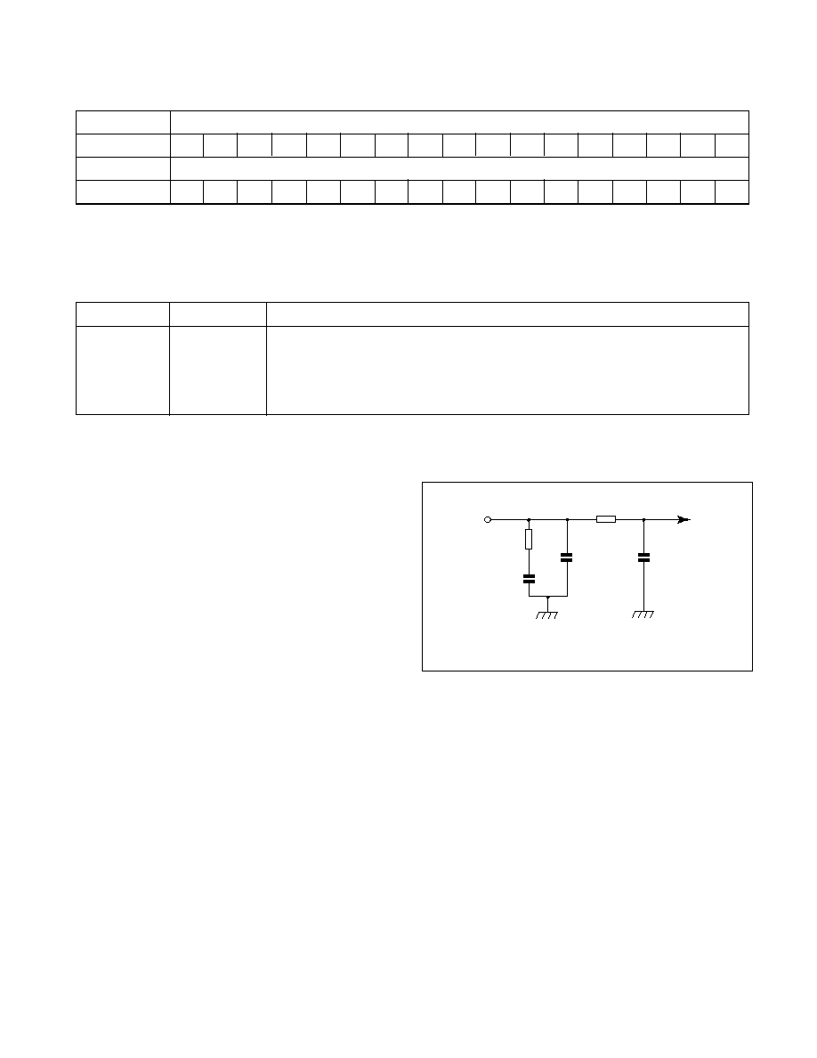
APPLICATIONS INFORMATION
By using constant current charge pumps the synthesiser
loop filter is purely passive. See Fig.8.
It is recommended that the primary filter is placed as close
to the synthesiser circuit as possible to minimise interference
caused by charge pump current pulses. The high frequency
clean-up filter, if needed at all, can be placed nearer the VCO
as required for board layout.
Suggested component values for
kHz comparison
frequency with a 5MHz/volt VCO are:
R1 = 15k
C1 = 220nF
CP = 18nF
RF = 47k
CF = 1.8nF
CP
R1
C1
CF
To VCO
PDOUT
PRELIMINARY
FILTER
RF
Fig.8 Typical synthesiser loop filter

www.zarlink.com
Information relating to products and services furnished herein by Zarlink Semiconductor Inc. or its subsidiaries (collectively "Zarlink") is believed to be reliable.
However, Zarlink assumes no liability for errors that may appear in this publication, or for liability otherwise arising from the application or use of any such
information, product or service or for any infringement of patents or other intellectual property rights owned by third parties which may result from such application or
use. Neither the supply of such information or purchase of product or service conveys any license, either express or implied, under patents or other intellectual
property rights owned by Zarlink or licensed from third parties by Zarlink, whatsoever. Purchasers of products are also hereby notified that the use of product in
certain ways or in combination with Zarlink, or non-Zarlink furnished goods or services may infringe patents or other intellectual property rights owned by Zarlink.
This publication is issued to provide information only and (unless agreed by Zarlink in writing) may not be used, applied or reproduced for any purpose nor form part
of any order or contract nor to be regarded as a representation relating to the products or services concerned. The products, their specifications, services and other
information appearing in this publication are subject to change by Zarlink without notice. No warranty or guarantee express or implied is made regarding the
capability, performance or suitability of any product or service. Information concerning possible methods of use is provided as a guide only and does not constitute
any guarantee that such methods of use will be satisfactory in a specific piece of equipment. It is the user's responsibility to fully determine the performance and
suitability of any equipment using such information and to ensure that any publication or data used is up to date and has not been superseded. Manufacturing does
not necessarily include testing of all functions or parameters. These products are not suitable for use in any medical products whose failure to perform may result in
significant injury or death to the user. All products and materials are sold and services provided subject to Zarlink's conditions of sale which are available on request.
Purchase of Zarlink's I
2
C components conveys a licence under the Philips I
2
C Patent rights to use these components in and I
2
C System, provided that the system
conforms to the I
2
C Standard Specification as defined by Philips.
Zarlink, ZL and the Zarlink Semiconductor logo are trademarks of Zarlink Semiconductor Inc.
Copyright Zarlink Semiconductor Inc. All Rights Reserved.
TECHNICAL DOCUMENTATION - NOT FOR RESALE
For more information about all Zarlink products
visit our Web Site at