
1
Zarlink Semiconductor Inc.
Zarlink, ZL and the Zarlink Semiconductor logo are trademarks of Zarlink Semiconductor Inc.
Copyright 2004, Zarlink Semiconductor Inc. All Rights Reserved.
Features
� Synchronizes to clock-and-sync-pair to maintain
minimal phase skew between an H.110 primary
master clock and a secondary master clock
� Supports Telcordia GR-1244-CORE Stratum 4 and
4E
� Supports ITU-T G.823 and G.824 for 2048 kbit/s
and 1544 kbit/s interfaces
� Supports ANSI T1.403 and ETSI ETS 300 011 for
ISDN primary rate interfaces
� Simple hardware control interface
� Manual and Automatic hitless reference switching
� Accepts three input references and synchronizes
to any combination of 8 kHz, 1.544 MHz,
2.048 MHz, 8.192 MHz or 16.384 MHz inputs
� Provides a range of clock outputs: 1.544 MHz,
2.048 MHz, 3.088 MHz, 6.312 MHz, 16.384 MHz
and either 4.096 MHz and 8.192 MHz or
32.768 MHz and 65.536 MHz
� Provides 5 styles of 8 kHz framing pulses
� Holdover frequency accuracy of 1x10
-7
� Provides Lock, Holdover and selectable Out of
Range indication
� Attenuates wander from 1.8 Hz
� Less than 0.6 ns
pp
intrinsic jitter on all output
clocks
� External master clock source: Clock Oscillator or
Crystal
Applications
� Synchronization and timing control for multi-trunk
DS1/ E1 terminal systems such as DSLAMs,
Gateways and PBXs
� Clock and frame pulse source for H.110 CT Bus,
ST-BUS, GCI and other time division multiplex
(TDM) buses
October 2004
Ordering Information
ZL30102QDG
64 pin TQFP
-40
�C to +85�C
ZL30102
T1/E1 Stratum 4/4E Redundant System
Clock Synchronizer for DS1/E1 and H.110
Data Sheet
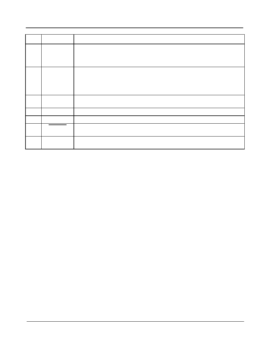
Figure 1 - Functional Block Diagram
Reference
Monitor
Mode
Control
Virtual
Reference
IEEE
1149.1a
TIE
Corrector
Enable
State Machine
Frequency
Select
MUX
TIE
Corrector
Circuit
MODE_SEL1:0
TCK
REF1
RST
REF_SEL1:0
TIE_CLR
C1.5o
C4/C65o
C8/C32o
C16o
F4/F65o
F8/F32o
F16o
OSCo
OSCi
Master Clock
TDO
REF0
TDI TMS
TRST
HOLDOVER
FASTLOCK
HMS
LOCK
REF_FAIL0
REF_FAIL1
DPLL
OUT_SEL
OOR_SEL
C2o
REF_FAIL2
REF2
REF2_SYNC
SEC_MSTR
E1
Synthesizer
DS1
Synthesizer
MUX
DS2
Synthesizer
C3o
C6o

ZL30102
Data Sheet
2
Zarlink Semiconductor Inc.
Description
The ZL30102 DS1/E1 Synchronizer contains a digital phase-locked loop (DPLL), which provides timing and
synchronization for DS1/E1 transmission equipment deploying redundant network clocks.
The ZL30102 generates ST-BUS and other TDM clock and framing signals that are phase locked to one of three
network references or to another system master-clock reference. It helps ensure system reliability by monitoring its
references for frequency accuracy and stability and by maintaining a tight phase alignment between the primary
master-clock and secondary master clock outputs even in the presence of high network jitter.
The ZL30102 is intended to be the central timing and synchronization resource for network equipment that
complies with Telcordia, ETSI, ITU-T and ANSI network specifications.

ZL30102
Data Sheet
Table of Contents
3
Zarlink Semiconductor Inc.
1.0 Change Summary . . . . . . . . . . . . . . . . . . . . . . . . . . . . . . . . . . . . . . . . . . . . . . . . . . . . . . . . . . . . . . . . . . . . . . 7
2.0 Physical Description . . . . . . . . . . . . . . . . . . . . . . . . . . . . . . . . . . . . . . . . . . . . . . . . . . . . . . . . . . . . . . . . . . . . 8
2.1 Pin Connections . . . . . . . . . . . . . . . . . . . . . . . . . . . . . . . . . . . . . . . . . . . . . . . . . . . . . . . . . . . . . . . . . . . . . 8
2.2 Pin Description . . . . . . . . . . . . . . . . . . . . . . . . . . . . . . . . . . . . . . . . . . . . . . . . . . . . . . . . . . . . . . . . . . . . . . 9
3.0 Functional Description . . . . . . . . . . . . . . . . . . . . . . . . . . . . . . . . . . . . . . . . . . . . . . . . . . . . . . . . . . . . . . . . . 13
3.1 Reference Select Multiplexer (MUX) . . . . . . . . . . . . . . . . . . . . . . . . . . . . . . . . . . . . . . . . . . . . . . . . . . . . . 13
3.2 Reference Monitor . . . . . . . . . . . . . . . . . . . . . . . . . . . . . . . . . . . . . . . . . . . . . . . . . . . . . . . . . . . . . . . . . . . 13
3.3 Time Interval Error (TIE) Corrector Circuit. . . . . . . . . . . . . . . . . . . . . . . . . . . . . . . . . . . . . . . . . . . . . . . . . 16
3.4 Digital Phase Lock Loop (DPLL) . . . . . . . . . . . . . . . . . . . . . . . . . . . . . . . . . . . . . . . . . . . . . . . . . . . . . . . . 19
3.5 Frequency Synthesizers . . . . . . . . . . . . . . . . . . . . . . . . . . . . . . . . . . . . . . . . . . . . . . . . . . . . . . . . . . . . . . 20
3.6 State Machine . . . . . . . . . . . . . . . . . . . . . . . . . . . . . . . . . . . . . . . . . . . . . . . . . . . . . . . . . . . . . . . . . . . . . . 20
3.7 Master Clock . . . . . . . . . . . . . . . . . . . . . . . . . . . . . . . . . . . . . . . . . . . . . . . . . . . . . . . . . . . . . . . . . . . . . . . 20
4.0 Control and Modes of Operation . . . . . . . . . . . . . . . . . . . . . . . . . . . . . . . . . . . . . . . . . . . . . . . . . . . . . . . . . 21
4.1 Out of Range Selection . . . . . . . . . . . . . . . . . . . . . . . . . . . . . . . . . . . . . . . . . . . . . . . . . . . . . . . . . . . . . . . 21
4.2 Loop Filter and Limiter Selection . . . . . . . . . . . . . . . . . . . . . . . . . . . . . . . . . . . . . . . . . . . . . . . . . . . . . . . . 21
4.3 Output Clock and Frame Pulse Selection . . . . . . . . . . . . . . . . . . . . . . . . . . . . . . . . . . . . . . . . . . . . . . . . . 21
4.4 Modes of Operation . . . . . . . . . . . . . . . . . . . . . . . . . . . . . . . . . . . . . . . . . . . . . . . . . . . . . . . . . . . . . . . . . . 21
4.4.1 Freerun Mode. . . . . . . . . . . . . . . . . . . . . . . . . . . . . . . . . . . . . . . . . . . . . . . . . . . . . . . . . . . . . . . . . . 22
4.4.2 Holdover Mode. . . . . . . . . . . . . . . . . . . . . . . . . . . . . . . . . . . . . . . . . . . . . . . . . . . . . . . . . . . . . . . . . 22
4.4.3 Normal Mode . . . . . . . . . . . . . . . . . . . . . . . . . . . . . . . . . . . . . . . . . . . . . . . . . . . . . . . . . . . . . . . . . . 23
4.4.4 Automatic Mode . . . . . . . . . . . . . . . . . . . . . . . . . . . . . . . . . . . . . . . . . . . . . . . . . . . . . . . . . . . . . . . . 24
4.5 Reference Switching . . . . . . . . . . . . . . . . . . . . . . . . . . . . . . . . . . . . . . . . . . . . . . . . . . . . . . . . . . . . . . . . . 24
4.5.1 Manual Reference Switching . . . . . . . . . . . . . . . . . . . . . . . . . . . . . . . . . . . . . . . . . . . . . . . . . . . . . . 24
4.5.2 Automatic Reference Switching . . . . . . . . . . . . . . . . . . . . . . . . . . . . . . . . . . . . . . . . . . . . . . . . . . . . 25
4.5.2.1 Automatic Reference Switching - Coarse Reference Failure . . . . . . . . . . . . . . . . . . . . . . . . . 26
4.5.2.2 Automatic Reference Switching - Reference Frequency Out-of-Range . . . . . . . . . . . . . . . . . 27
4.6 Clock Redundancy Support. . . . . . . . . . . . . . . . . . . . . . . . . . . . . . . . . . . . . . . . . . . . . . . . . . . . . . . . . . . . 28
5.0 Measures of Performance . . . . . . . . . . . . . . . . . . . . . . . . . . . . . . . . . . . . . . . . . . . . . . . . . . . . . . . . . . . . . . . 32
5.1 Jitter. . . . . . . . . . . . . . . . . . . . . . . . . . . . . . . . . . . . . . . . . . . . . . . . . . . . . . . . . . . . . . . . . . . . . . . . . . . . . . 32
5.2 Jitter Generation (Intrinsic Jitter) . . . . . . . . . . . . . . . . . . . . . . . . . . . . . . . . . . . . . . . . . . . . . . . . . . . . . . . . 32
5.3 Jitter Tolerance . . . . . . . . . . . . . . . . . . . . . . . . . . . . . . . . . . . . . . . . . . . . . . . . . . . . . . . . . . . . . . . . . . . . . 32
5.4 Jitter Transfer . . . . . . . . . . . . . . . . . . . . . . . . . . . . . . . . . . . . . . . . . . . . . . . . . . . . . . . . . . . . . . . . . . . . . . 32
5.5 Frequency Accuracy . . . . . . . . . . . . . . . . . . . . . . . . . . . . . . . . . . . . . . . . . . . . . . . . . . . . . . . . . . . . . . . . . 32
5.6 Holdover Accuracy . . . . . . . . . . . . . . . . . . . . . . . . . . . . . . . . . . . . . . . . . . . . . . . . . . . . . . . . . . . . . . . . . . 32
5.7 Pull-in Range . . . . . . . . . . . . . . . . . . . . . . . . . . . . . . . . . . . . . . . . . . . . . . . . . . . . . . . . . . . . . . . . . . . . . . . 33
5.8 Lock Range . . . . . . . . . . . . . . . . . . . . . . . . . . . . . . . . . . . . . . . . . . . . . . . . . . . . . . . . . . . . . . . . . . . . . . . . 33
5.9 Phase Slope . . . . . . . . . . . . . . . . . . . . . . . . . . . . . . . . . . . . . . . . . . . . . . . . . . . . . . . . . . . . . . . . . . . . . . . 33
5.10 Time Interval Error (TIE) . . . . . . . . . . . . . . . . . . . . . . . . . . . . . . . . . . . . . . . . . . . . . . . . . . . . . . . . . . . . . 33
5.11 Maximum Time Interval Error (MTIE) . . . . . . . . . . . . . . . . . . . . . . . . . . . . . . . . . . . . . . . . . . . . . . . . . . . 33
5.12 Phase Continuity . . . . . . . . . . . . . . . . . . . . . . . . . . . . . . . . . . . . . . . . . . . . . . . . . . . . . . . . . . . . . . . . . . . 33
5.13 Lock Time . . . . . . . . . . . . . . . . . . . . . . . . . . . . . . . . . . . . . . . . . . . . . . . . . . . . . . . . . . . . . . . . . . . . . . . . 33
6.0 Applications . . . . . . . . . . . . . . . . . . . . . . . . . . . . . . . . . . . . . . . . . . . . . . . . . . . . . . . . . . . . . . . . . . . . . . . . . . 34
6.1 Power Supply Decoupling . . . . . . . . . . . . . . . . . . . . . . . . . . . . . . . . . . . . . . . . . . . . . . . . . . . . . . . . . . . . . 34
6.2 Master Clock . . . . . . . . . . . . . . . . . . . . . . . . . . . . . . . . . . . . . . . . . . . . . . . . . . . . . . . . . . . . . . . . . . . . . . . 34
6.2.1 Clock Oscillator . . . . . . . . . . . . . . . . . . . . . . . . . . . . . . . . . . . . . . . . . . . . . . . . . . . . . . . . . . . . . . . . 35
6.2.2 Crystal Oscillator . . . . . . . . . . . . . . . . . . . . . . . . . . . . . . . . . . . . . . . . . . . . . . . . . . . . . . . . . . . . . . . 35
6.3 Power Up Sequence . . . . . . . . . . . . . . . . . . . . . . . . . . . . . . . . . . . . . . . . . . . . . . . . . . . . . . . . . . . . . . . . . 36
6.4 Reset Circuit . . . . . . . . . . . . . . . . . . . . . . . . . . . . . . . . . . . . . . . . . . . . . . . . . . . . . . . . . . . . . . . . . . . . . . . 36
6.5 Clock Redundancy System Architecture . . . . . . . . . . . . . . . . . . . . . . . . . . . . . . . . . . . . . . . . . . . . . . . . . . 37
7.0 Characteristics . . . . . . . . . . . . . . . . . . . . . . . . . . . . . . . . . . . . . . . . . . . . . . . . . . . . . . . . . . . . . . . . . . . . . . . . 38
7.1 AC and DC Electrical Characteristics . . . . . . . . . . . . . . . . . . . . . . . . . . . . . . . . . . . . . . . . . . . . . . . . . . . . 38

ZL30102
Data Sheet
Table of Contents
4
Zarlink Semiconductor Inc.
7.2 Performance Characteristics . . . . . . . . . . . . . . . . . . . . . . . . . . . . . . . . . . . . . . . . . . . . . . . . . . . . . . . . . . . 46

ZL30102
Data Sheet
List of Figures
5
Zarlink Semiconductor Inc.
Figure 1 - Functional Block Diagram . . . . . . . . . . . . . . . . . . . . . . . . . . . . . . . . . . . . . . . . . . . . . . . . . . . . . . . . . . . . 1
Figure 2 - Pin Connections (64 pin TQFP, please see Note 1) . . . . . . . . . . . . . . . . . . . . . . . . . . . . . . . . . . . . . . . . 8
Figure 3 - Reference Monitor Circuit . . . . . . . . . . . . . . . . . . . . . . . . . . . . . . . . . . . . . . . . . . . . . . . . . . . . . . . . . . . 14
Figure 4 - Behaviour of the Dis/Re-qualify Timer . . . . . . . . . . . . . . . . . . . . . . . . . . . . . . . . . . . . . . . . . . . . . . . . . . 14
Figure 5 - DS1 Out-of-Range Thresholds for OOR_SEL=0. . . . . . . . . . . . . . . . . . . . . . . . . . . . . . . . . . . . . . . . . . 15
Figure 6 - E1 Out-of-Range Thresholds for OOR_SEL=1 . . . . . . . . . . . . . . . . . . . . . . . . . . . . . . . . . . . . . . . . . . . 15
Figure 7 - REF2_SYNC Reference Monitor . . . . . . . . . . . . . . . . . . . . . . . . . . . . . . . . . . . . . . . . . . . . . . . . . . . . . . 16
Figure 8 - Timing Diagram of Hitless Reference Switching . . . . . . . . . . . . . . . . . . . . . . . . . . . . . . . . . . . . . . . . . . 17
Figure 9 - Timing Diagram of Hitless Mode Switching . . . . . . . . . . . . . . . . . . . . . . . . . . . . . . . . . . . . . . . . . . . . . . 18
Figure 10 - DPLL Block Diagram . . . . . . . . . . . . . . . . . . . . . . . . . . . . . . . . . . . . . . . . . . . . . . . . . . . . . . . . . . . . . . 19
Figure 11 - Mode Switching in Normal Mode . . . . . . . . . . . . . . . . . . . . . . . . . . . . . . . . . . . . . . . . . . . . . . . . . . . . . 23
Figure 12 - Reference Switching in Normal Mode . . . . . . . . . . . . . . . . . . . . . . . . . . . . . . . . . . . . . . . . . . . . . . . . . 24
Figure 13 - Reference Selection in Automatic Mode (MODE_SEL=11). . . . . . . . . . . . . . . . . . . . . . . . . . . . . . . . . 25
Figure 14 - Mode Switching in Automatic Mode . . . . . . . . . . . . . . . . . . . . . . . . . . . . . . . . . . . . . . . . . . . . . . . . . . 26
Figure 15 - Automatic Reference Switching - Coarse Reference Failure . . . . . . . . . . . . . . . . . . . . . . . . . . . . . . . 27
Figure 16 - Automatic Reference Switching - Out-of-Range Reference Failure . . . . . . . . . . . . . . . . . . . . . . . . . . 28
Figure 17 - Examples of REF2 & REF2_SYNC to Output Alignment . . . . . . . . . . . . . . . . . . . . . . . . . . . . . . . . . . 29
Figure 18 - Clock Redundancy with Two Independent Timing Cards . . . . . . . . . . . . . . . . . . . . . . . . . . . . . . . . . . 30
Figure 19 - Recommended Power Supply Decoupling . . . . . . . . . . . . . . . . . . . . . . . . . . . . . . . . . . . . . . . . . . . . . 34
Figure 20 - Clock Oscillator Circuit. . . . . . . . . . . . . . . . . . . . . . . . . . . . . . . . . . . . . . . . . . . . . . . . . . . . . . . . . . . . . 35
Figure 21 - Crystal Oscillator Circuit . . . . . . . . . . . . . . . . . . . . . . . . . . . . . . . . . . . . . . . . . . . . . . . . . . . . . . . . . . . 36
Figure 22 - Power-Up Reset Circuit . . . . . . . . . . . . . . . . . . . . . . . . . . . . . . . . . . . . . . . . . . . . . . . . . . . . . . . . . . . . 36
Figure 23 - Typical Clocking Architecture of an ECTF H.110 System . . . . . . . . . . . . . . . . . . . . . . . . . . . . . . . . . . 37
Figure 24 - Timing Parameter Measurement Voltage Levels. . . . . . . . . . . . . . . . . . . . . . . . . . . . . . . . . . . . . . . . . 39
Figure 25 - REF0/1/2 Input Timing and Input to Output Timing . . . . . . . . . . . . . . . . . . . . . . . . . . . . . . . . . . . . . . . 40
Figure 26 - REF2_SYNC Timing . . . . . . . . . . . . . . . . . . . . . . . . . . . . . . . . . . . . . . . . . . . . . . . . . . . . . . . . . . . . . . 40
Figure 27 - E1 Output Timing Referenced to F8/F32o. . . . . . . . . . . . . . . . . . . . . . . . . . . . . . . . . . . . . . . . . . . . . . 43
Figure 28 - DS1 Output Timing Referenced to F8/F32o . . . . . . . . . . . . . . . . . . . . . . . . . . . . . . . . . . . . . . . . . . . . 44
Figure 29 - DS2 Output Timing Referenced to F8/F32o . . . . . . . . . . . . . . . . . . . . . . . . . . . . . . . . . . . . . . . . . . . . 44

ZL30102
Data Sheet
List of Tables
6
Zarlink Semiconductor Inc.
Table 1 - Out of Range Limits Selection. . . . . . . . . . . . . . . . . . . . . . . . . . . . . . . . . . . . . . . . . . . . . . . . . . . . . . . . . 21
Table 2 - Loop Filter and Limiter Settings . . . . . . . . . . . . . . . . . . . . . . . . . . . . . . . . . . . . . . . . . . . . . . . . . . . . . . . 21
Table 3 - Clock and Frame Pulse Selection with OUT_SEL Pin . . . . . . . . . . . . . . . . . . . . . . . . . . . . . . . . . . . . . . 21
Table 4 - Operating Modes. . . . . . . . . . . . . . . . . . . . . . . . . . . . . . . . . . . . . . . . . . . . . . . . . . . . . . . . . . . . . . . . . . . 22
Table 5 - Manual Reference Selection . . . . . . . . . . . . . . . . . . . . . . . . . . . . . . . . . . . . . . . . . . . . . . . . . . . . . . . . . . 24
Table 6 - The Reference Selection Pins in the Automatic Mode (MODE_SEL=11) . . . . . . . . . . . . . . . . . . . . . . . . 25
Table 7 - Typical Clock Oscillator Specification . . . . . . . . . . . . . . . . . . . . . . . . . . . . . . . . . . . . . . . . . . . . . . . . . . . 35
Table 8 - Typical Crystal Oscillator Specification . . . . . . . . . . . . . . . . . . . . . . . . . . . . . . . . . . . . . . . . . . . . . . . . . . 35

ZL30102
Data Sheet
7
Zarlink Semiconductor Inc.
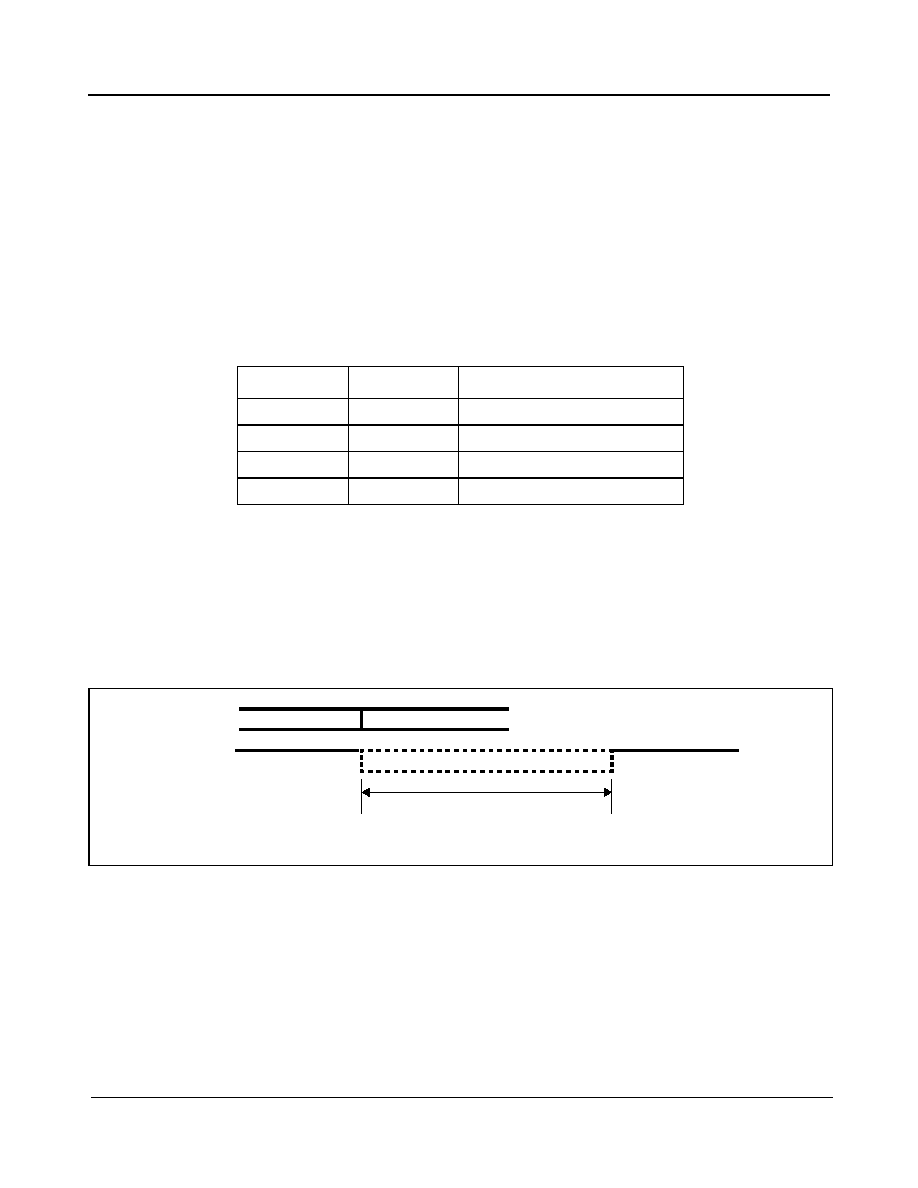
1.0 Change Summary
Changes from July 2004 Issue to October 2004 Issue. Page, section, figure and table numbers refer to this issue.
Page
Item
Change
8
Figure 2
Added note specifying not e-Pad
19
Section 3.3
Changed 20 ns to 200 ns in "HMS=0" section
38
Table "DC Electrical Characteristics*"
Corrected current consumption
Corrected V
t-
input voltage characteristic
41
Table "AC Electrical Characteristics* -
Input to output timing for REF0, REF1
and REF2 references when
TIE_CLR = 0 (see Figure 25)."
Corrected Min. Max. values
42
Section 7.1
Corrected pulse widths
47
Section 7.2
Corrected jitter numbers

ZL30102
Data Sheet
8
Zarlink Semiconductor Inc.
2.0 Physical Description
2.1 Pin Connections
Figure 2 - Pin Connections (64 pin TQFP, please see Note 1)
Note 1: The ZL30102 uses the TQFP shown in the package outline designated with the suffix QD, the ZL30102
does not use the e-Pad TQFP.
ZL30102
34
36
38
40
42
44
46
48
64
62
60
58
56
52
50
54
16
14
12
10
8
6
4
2
OSCo
NC
GND
OUT_SEL
C1.5o
MODE_SEL1
V
DD
AV
DD
IC
C3o
RST
C6o
V
CORE
LOCK
HMS
TRS
T
GND
TDO
TMS
HOLDOVER
REF_F
A
IL1
TCK
AGND
F4/F65o
V
DD
REF0
REF2
NC
IC
FASTLOCK
C8/C32o
NC
C2o
AGND
AV
DD
NC
F8/
F
32
o
C4/C65o
REF_SEL0
18
20
22
24
26
30
32
28
C16o
F16o
TIE_CLR
OOR_SEL
SEC_MSTR
TDI
OSCi
V
CORE
AV
DD
AV
DD
AV
DD
AV
CORE
AV
CORE
GND
AGND
AGND
AGND
REF_F
A
IL0
REF1
REF2_SYNC
IC
IC
MODE_SEL0
REF_F
A
IL2
REF_SEL1

ZL30102
Data Sheet
9
Zarlink Semiconductor Inc.
2.2 Pin Description
Pin #
Name
Description
1
GND
Ground. 0 V
2
V
CORE
Positive Supply Voltage. +1.8 V
DC
nominal
3
LOCK
Lock Indicator (Output). This output goes to a logic high when the PLL is frequency
locked to the selected input reference.
4
HOLDOVER
Holdover (Output). This output goes to a logic high whenever the PLL goes into
holdover mode.
5
REF_FAIL0
Reference 0 Failure Indicator (Output). A logic high at this pin indicates that the REF0
reference frequency has exceeded the out-of-range limit set by the OOR_SEL pin or that
it is exhibiting abrupt phase or frequency changes.
6
REF_FAIL1
Reference 1 Failure Indicator (Output). A logic high at this pin indicates that the REF1
reference frequency has exceeded the out-of-range limit set by the OOR_SEL pin or that
it is exhibiting abrupt phase or frequency changes.
7
REF_FAIL2
Reference 2 Failure Indicator (Output). A logic high at this pin indicates that the REF2
reference frequency has exceeded the out-of-range limit set by the OOR_SEL pin or that
it is exhibiting abrupt phase or frequency changes.
8
TDO
Test Serial Data Out (Output). JTAG serial data is output on this pin on the falling edge
of TCK. This pin is held in high impedance state when JTAG scan is not enabled.
9
TMS
Test Mode Select (Input). JTAG signal that controls the state transitions of the TAP
controller. This pin is internally pulled up to V
DD
. If this pin is not used then it should be
left unconnected.
10
TRST
Test Reset (Input). Asynchronously initializes the JTAG TAP controller by putting it in
the Test-Logic-Reset state. This pin should be pulsed low on power-up to ensure that
the device is in the normal functional state. This pin is internally pulled up to V
DD
. If
this pin is not used then it should be connected to GND.
11
TCK
Test Clock (Input): Provides the clock to the JTAG test logic. If this pin is not used then it
should be pulled down to GND.
12
V
CORE
Positive Supply Voltage. +1.8 V
DC
nominal
13
GND
Ground. 0 V
14
AV
CORE
Positive Analog Supply Voltage. +1.8 V
DC
nominal
15
TDI
Test Serial Data In (Input). JTAG serial test instructions and data are shifted in on this
pin. This pin is internally pulled up to V
DD
. If this pin is not used then it should be left
unconnected.
16
HMS
Hitless Mode Switching (Input). The HMS input controls phase accumulation during the
transition from Holdover or Freerun mode to Normal mode on the same reference. A logic
low at this pin will cause the ZL30102 to maintain the delay stored in the TIE corrector
circuit when it transitions from Holdover or Freerun mode to Normal mode. A logic high
on this pin will cause the ZL30102 to measure a new delay for its TIE corrector circuit
thereby minimizing the output phase movement when it transitions from Holdover or
Freerun mode to Normal mode.
17
MODE_SEL0 Mode Select 0 (Input). This input combined with MODE_SEL1 determines the mode of
operation, see Table 4 on page 22.
18
MODE_SEL1 Mode Select 1 (Input). See MODE_SEL0 pin description.

ZL30102
Data Sheet
10
Zarlink Semiconductor Inc.
19
RST
Reset (Input). A logic low at this input resets the device. On power up, the RST pin
must be held low for a minimum of 300 ns after the power supply pins have reached
the minimum supply voltage. When the RST pin goes high, the device will transition
into a Reset state for 3 ms. In the Reset state all outputs will be forced into high
impedance.
20
OSCo
Oscillator Master Clock (Output). For crystal operation, a 20 MHz crystal is connected
from this pin to OSCi. This output is not suitable for driving other devices. For clock
oscillator operation, this pin must be left unconnected.
21
OSCi
Oscillator Master Clock (Input). For crystal operation, a 20 MHz crystal is connected
from this pin to OSCo. For clock oscillator operation, this pin must be connected to a
clock source.
22
IC
Internal Connection. Leave unconnected.
23
GND
Ground. 0 V
24
NC
No internal bonding Connection. Leave unconnected.
25
V
DD
Positive Supply Voltage. +3.3 V
DC
nominal
26
OUT_SEL
Output Selection (Input). This input selects the signals on the combined output clock
and frame pulse pins, see Table 3 on page 21.
27
IC
Internal Connection. Connect this pin to ground.
28
IC
Internal Connection. Connect this pin to ground.
29
AV
DD
Positive Analog Supply Voltage. +3.3 V
DC
nominal
30
C6o
Clock 6.312 MHz (Output). This output is used in DS2 applications.
31
C3o
Clock 3.088 MHz (Output). This output is used in DS1 applications.
32
C1.5o
Clock 1.544 MHz (Output). This output is used in DS1 applications.
This clock output pad includes a Schmitt input which serves as a PLL feedback path;
proper transmission-line termination should be applied to maintain reflections below
Schmitt trigger levels.
33
AGND
Analog Ground. 0 V
34
AGND
Analog Ground. 0 V
35
AV
CORE
Positive Analog Supply Voltage. +1.8 V
DC
nominal
36
AV
DD
Positive Analog Supply Voltage. +3.3 V
DC
nominal
37
AV
DD
Positive Analog Supply Voltage. +3.3 V
DC
nominal
38
NC
No internal bonding Connection. Leave unconnected.
39
NC
No internal bonding Connection. Leave unconnected.
40
AGND
Analog Ground. 0 V
41
AGND
Analog Ground. 0 V
42
C4/C65o
Clock 4.096 MHz or 65.536 MHz (Output). This output is used for ST-BUS operation at
2.048 Mbit/s, 4.096 Mbit/s or 65.536 MHz (ST-BUS 65.536 Mbit/s). The output frequency
is selected via the OUT_SEL pin, see Table 3 on page 21.
Pin #
Name
Description

ZL30102
Data Sheet
11
Zarlink Semiconductor Inc.
43
C8/C32o
Clock 8.192 MHz or 32.768 MHz (Output). This output is used for ST-BUS and GCI
operation at 8.192 Mb/s or for operation with a 32.768 MHz clock. The output frequency
is selected via the OUT_SEL pin, see Table 3 on page 21.
In C8 mode, this clock output pad uses an included Schmitt input as a PLL feedback
path; proper transmission-line termination should be applied to maintain reflections below
Schmitt trigger levels.
44
AV
DD
Positive Analog Supply Voltage. +3.3 V
DC
nominal
45
AV
DD
Positive Analog Supply Voltage. +3.3 V
DC
nominal
46
C2o
Clock 2.048 MHz (Output). This output is used for standard E1 interface timing and for
ST-BUS operation at 2.048 Mbit/s.
This clock output pad includes a Schmitt input which serves as a PLL feedback path;
proper transmission-line termination should be applied to maintain reflections below
Schmitt trigger levels.
47
C16o
Clock 16.384 MHz (Output). This output is used for ST-BUS operation with a
16.384 MHz clock.
This clock output pad includes a Schmitt input which serves as a PLL feedback path;
proper transmission-line termination should be applied to maintain reflections below
Schmitt trigger levels.
48
F8/F32o
Frame Pulse (Output). This is an 8 kHz 122 ns active high framing pulse or it is an 8 kHz
31 ns active high framing pulse, which marks the beginning of a frame. The pulse width is
selected via the OUT_SEL pin, see Table 3 on page 21.
49
F4/F65o
Frame Pulse ST-BUS 2.048 Mbit/s or ST-BUS at 65.536 MHz clock (Output). This
output is an 8 kHz 244 ns active low framing pulse which marks the beginning of an ST-
BUS frame. This is typically used for ST-BUS operation at 2.048 Mbit/s and 4.096 Mbit/s.
Or this output is an 8 kHz 15 ns active low framing pulse, typically used for ST-BUS
operation with a clock rate of 65.536 MHz. The pulse width is selected via the OUT_SEL
pin, see Table 3 on page 21.
50
F16o
Frame Pulse ST-BUS 8.192 Mbit/s (Output). This is an 8 kHz 61 ns active low framing
pulse, which marks the beginning of an ST-BUS frame. This is typically used for ST-BUS
operation at 8.192 Mbit/s.
51
AGND
Analog Ground. 0 V
52
IC
Internal Connection. Connect this pin to ground.
53
REF_SEL0
Reference Select 0 (Input/Output). In the manual mode of operation, REF_SEL0 is an
input. As an input REF_SEL0 combined with REF_SEL1 selects the reference input that
is used for synchronization, see Table 6 on page 25.
In the Automatic mode of operation, REFSEL0 is an output indicating which of the input
references is the being selected. This pin is internally pulled down to GND.
54
REF_SEL1
Reference Select 1 (Input/Output). See REF_SEL0 pin description.
55
REF0
Reference (Input). This is one of three (REF0, REF1 and REF2) input reference sources
used for synchronization. One of five possible frequencies may be used: 8 kHz,
1.544 MHz, 2.048 MHz, 8.192 MHz or 16.384 MHz. This pin is internally pulled down to
GND.
56
REF1
Reference (Input). See REF0 pin description.
57
REF2
Reference (Input). See REF0 pin description.
Pin #
Name
Description
ZL30102
Data Sheet
12
Zarlink Semiconductor Inc.
58
REF2_SYNC REF2 Synchronization Frame Pulse (Input). This is the 8 kHz frame pulse
synchronization input associated with the REF2 reference. While the PLL is locked to the
REF2 input reference the output (multi) frame pulses are synchronized to this input. This
pin is internally pulled down to GND.
59
SEC_MSTR
Secondary Master Mode Selection (Input). A logic low at this pin selects the Primary
Master mode of operation with 1.8 Hz DPLL loop filter bandwidth. A logic high selects
Secondary Master mode which forces the PLL to clear its TIE corrector circuit and lock to
the selected reference using a high bandwidth loop filter and a phase slope limiting of
9.5 ms/s.
60
OOR_SEL
Out Of Range Selection (Input). This input selects the frequency out of range limits of
the reference inputs, see Table 1 on page 21.
61
V
DD
Positive Supply Voltage. +3.3 V
DC
nominal
62
NC
No internal bonding Connection. Leave unconnected.
63
TIE_CLR
TIE Circuit Reset (Input). A logic low at this input resets the Time Interval Error (TIE)
correction circuit resulting in a realignment of input phase with output phase.
64
FASTLOCK
Fast Lock (Input). Set temporarily high to allow the ZL30102 to quickly lock to the input
reference (one second locking time).
Pin #
Name
Description

ZL30102
Data Sheet
13
Zarlink Semiconductor Inc.
3.0 Functional Description
The ZL30102 is an SDH/PDH Synchronizer for Redundant System Clocks, providing timing and synchronization
signals to interface circuits for the following types of primary rate digital transmission links, see Table 1:
� DS1 compliant with ANSI T1.403 and Telcordia GR-1244-CORE Stratum 4/4E
� E1 compliant with ITU-T G.703 and ETSI ETS 300 011
Figure 1 is a functional block diagram of the ZL30102 which is described in the following sections.
3.1 Reference Select Multiplexer (MUX)
The ZL30102 accepts three simultaneous reference input signals and operates on their rising edges. One of them,
the primary reference (REF0), the secondary reference (REF1) or the tertiary reference (REF2) signal is selected
as input to the TIE Corrector Circuit based on the Reference Selection (REF_SEL1:0) inputs.
The use of the combined REF2 and REF2_SYNC inputs allows for a very accurate phase alignment of the output
frame pulses to the 8 kHz frame pulse supplied to the REF2_SYNC input. This feature supports the implementation
of Primary and Secondary Master system clocks in H.110 systems.
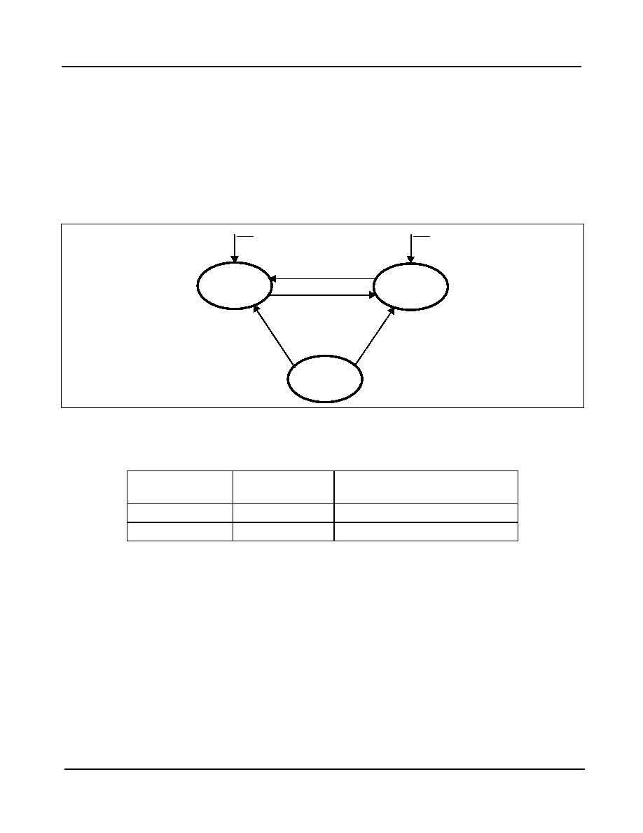
3.2 Reference Monitor
The input references are monitored by three independent reference monitor blocks, one for each reference. The
block diagram of a single reference monitor is shown in Figure 3. For each reference clock, the frequency is
detected and the clock is continuously monitored for three independent criteria that indicate abnormal behavior of
the reference signal, for example; long term drift from its nominal frequency or excessive jitter. To ensure proper
operation of the reference monitor circuit, the minimum input pulse width restriction of 15 nsec must be
observed.
� Reference Frequency Detector (RFD): This detector determines whether the frequency of the reference
clock is 8 kHz, 1.544 MHz, 2.048 MHz 8.192 MHz or 16.384 MHz and provides this information to the
various monitor circuits and the phase detector circuit of the DPLL.
� Precise Frequency Monitor (PFM): This circuit determines whether the frequency of the reference clock
is within the selected accuracy range, see Table 1.
� Coarse Frequency Monitor (CFM): This circuit monitors the reference frequency over intervals of
approximately 30
�s to quickly detect large frequency changes.
� Single Cycle Monitor (SCM): This detector checks the period of a single clock cycle to detect large
phase hits or the complete loss of the clock.

ZL30102
Data Sheet
14
Zarlink Semiconductor Inc.
Figure 3 - Reference Monitor Circuit
Exceeding the thresholds of any of the monitors forces the corresponding REF_FAIL pin to go high. The single
cycle and coarse frequency failure flags force the DPLL into Holdover mode and feed a timer that disqualifies the
reference input signal when the failures are present for more than 2.5 s. The single cycle and coarse frequency
failures must be absent for 10 s to let the timer re-qualify the input reference signal as valid. Multiple failures of less
than 2.5 s each have an accumulative effect and will disqualify the reference eventually. This is illustrated in Figure
4 where REF0 experiences disruptions while REF1 is stable.
Figure 4 - Behaviour of the Dis/Re-qualify Timer
Reference Frequency
Detector
Single Cycle
Monitor
Precise Frequency
Monitor
Coarse Frequency
Monitor
dis/re-qualify
timer
REF0 /
REF1 /
REF2
OR
OR
OR
REF_OOR = reference out of range.
REF_DIS= reference disrupted.
Both are internal signals.
Reference
select
state machine
REF_SEL1:0
REF_OOR
Mode select
state machine
HOLDOVER
REF_DIS
REF_FAIL0 /
REF_FAIL1 /
REF_FAIL2
2.5 s
10 s
REF0
dis/re-qualify
SCM or CFM failure
REF_FAIL0
HOLDOVER
REF_OOR0
(internal signal)
REF1
REF0
REF1
REF0
REF_SEL
timer on REF0
SCM or CFM failure

ZL30102
Data Sheet
15
Zarlink Semiconductor Inc.
When the incoming signal returns to normal (REF_FAIL=0), the DPLL returns to Normal mode with the output
signal locked to the input signal. Each of the monitors has a built-in hysteresis to prevent flickering of the REF_FAIL
status pin at the threshold boundaries. The precise frequency monitor and the timer do not affect the mode
(Holdover/Normal) of the DPLL.
If the device is set to Automatic mode (MODE_SEL1:0=11), then the state machine does not immediately switch to
another reference. If the single cycle and/or coarse frequency failures persist for more than 2.5 s or the precise
frequency monitor detects a failure, then the state machine will switch to another valid reference if that is available.
If there no other reference available, it stays in Holdover mode.
The precise frequency monitor's failure thresholds are selected with the OOR_SEL input based on the ZL30102
applications, Table 1. Figure 5 and Figure 6 show the out of range limits for various master clock accuracies. It will
take the precise frequency monitor up to 10 s to qualify or disqualify the input reference.
Figure 5 - DS1 Out-of-Range Thresholds for OOR_SEL=0
Figure 6 - E1 Out-of-Range Thresholds for OOR_SEL=1
In addition to the monitoring of the REF2 reference signal the companion REF2_SYNC input signal is also
monitored for failure (see Figure 7).
C20 Clock Accuracy
0 ppm
+32 ppm
-32 ppm
0
51
83
64
32
32
-32
-96
-75
-50
0
-25
25
75
Frequency offset [ppm]
Out of Range
Out of Range
Out of Range
In Range
In Range
In Range
C20
50
-64
-83
115
96
-32
-51
-115
C20
C20
100
-100
C20: 20 MHz master oscillator clock
0 ppm
+50 ppm
-50 ppm
0
50
130
100
50
80
-50
-150
-150
-100
0
-50
50
150
Frequency offset [ppm]
Out of Range
Out of Range
Out of Range
In Range
In Range
In Range
C20
100
-100
-130
180
150
-50
-80
-180
C20
C20
-200
200
C20: 20 MHz master oscillator clock
C20 Clock Accuracy
ZL30102
Data Sheet
16
Zarlink Semiconductor Inc.
Sync Ratio Monitor (SRM): This monitor detects if the REF2_SYNC signal is an 8 kHz signal. It also checks the
number of REF2 reference clock cycles in a single REF2_SYNC frame pulse period to determine the integrity of the
REF2_SYNC signal, for example there must be exactly 256 clock cycles of a 2.048 MHz REF2 reference clock in a
single REF2_SYNC 8 kHz frame pulse period to validate the REF2_SYNC signal. If the REF2 and REF2_SYNC
inputs are selected for synchronization and the Sync Ratio Monitor detects a failure, the DPLL will abandon the
mechanism of aligning the output frame pulse to the REF2_SYNC pulse. Instead only the REF2 reference will be
used for synchronization.
Figure 7 - REF2_SYNC Reference Monitor
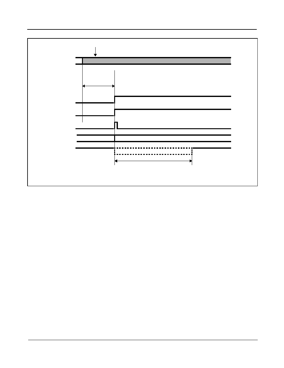
3.3 Time Interval Error (TIE) Corrector Circuit
The TIE Circuit eliminates phase transients on the output clock that may occur during reference switching or the
recovery from Holdover mode to Normal mode.
On recovery from Holdover mode (dependent on the HMS pin) or when switching to another reference input, the
TIE corrector circuit measures the phase delay between the current phase (feedback signal) and the phase of the
selected reference signal. This delay value is stored in the TIE corrector circuit. This circuit creates a new virtual
reference signal that is at the same phase position as the feedback signal. By using the virtual reference, the PLL
minimizes the phase transient it experiences when it recovers from Holdover mode.
The delay value can be reset by setting the TIE Corrector Circuit Clear pin (TIE_CLR) low for at least 15 ns. This
results in a phase alignment between the input reference signal and the output clocks and frame pulses as shown
in Figure 25. The speed of the phase alignment correction is limited by the selected loop filter bandwidth and the
phase slope limit (see Table 2). Convergence is always in the direction of least phase travel. TIE_CLR can be kept
low continuously; in that case the output clocks will always align with the selected input reference. This is illustrated
in Figure 8.
SYNC
Reference
Monitor
Circuit
to DPLL
REF2_SYNC
REF2
frequency
REF2

ZL30102
Data Sheet
17
Zarlink Semiconductor Inc.
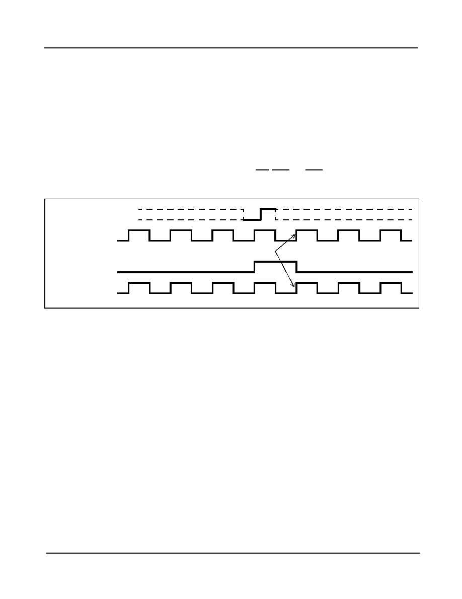
Figure 8 - Timing Diagram of Hitless Reference Switching
The Hitless Mode Switching (HMS) pin enables phase hitless returns from Freerun and Holdover modes to Normal
mode in a single reference operation. A logic low at the HMS input disables the TIE circuit updating the delay value
thereby forcing the output of the PLL to gradually move back to the original point before it went into Holdover mode.
(see Figure 9). This prevents accumulation of phase in network elements. A logic high (HMS=1) enables the TIE
circuit to update its delay value thereby preventing a large output phase movement after return to Normal mode.
This causes accumulation of phase in network elements. In both cases the PLL's output can be aligned with the
input reference by setting TIE_CLR low. Regardless of the HMS pin state, reference switching in the ZL30102 is
always hitless unless TIE_CLR is kept low continuously.
locked to REF1
REF0
Output
Clock
TIE_CLR = 1
TIE_CLR = 0
REF1
REF0
Output
Clock
REF1
locked to REF1
REF0
Output
Clock
REF1
REF0
Output
Clock
REF1
locked to REF0
locked to REF0

ZL30102
Data Sheet
18
Zarlink Semiconductor Inc.
Figure 9 - Timing Diagram of Hitless Mode Switching
Examples:
HMS=1: When ten Normal to Holdover to Normal mode transitions occur and in each case the Holdover mode was
entered for 2 seconds then the accumulated phase change (MTIE) could be as large as 2.13
�s.
- Phase
holdover_drift
= 0.1 ppm x 2 s = 200 ns
- Phase
mode_change
= 0 ns + 13 ns = 13 ns
- Phase
10 changes
= 10 x (200 ns + 13 ns) = 2.13
�s
REF
Phase drift in Holdover mode
HMS = 0
Normal mode
Return to Normal mode
REF
Output
Clock
REF
Output
Clock
REF
Output
Clock
Phase drift in Holdover mode
Normal mode
Return to Normal mode
Output
Clock
REF
Output
Clock
REF
Output
Clock
HMS = 1
TIE_CLR=0
REF
Output
Clock
TIE_CLR=0
REF
Output
Clock
ZL30102
Data Sheet
19
Zarlink Semiconductor Inc.
where:
- 0.1 ppm is the accuracy of the Holdover mode
- 0 ns is the maximum phase discontinuity in the transition from the Normal mode to the Holdover mode
- 13 ns is the maximum phase discontinuity in the transition from the Holdover mode to the Normal mode
when a new TIE corrector value is calculated
HMS=0: When the same ten Normal to Holdover to Normal mode changes occur and in each case Holdover mode
was entered for 2 seconds, then the overall MTIE would be 200 ns. As the delay value for the TIE corrector circuit is
not updated, there is no 13 ns measurement error at this point. The phase can still drift for 200 ns when the PLL is
in Holdover mode but when the PLL enters Normal mode again, the phase moves back to the original point so the
phase is not accumulated.
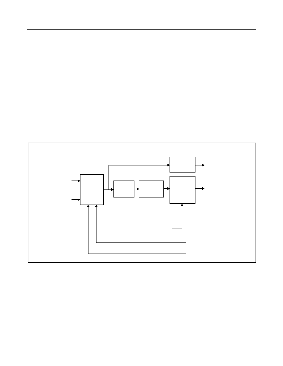
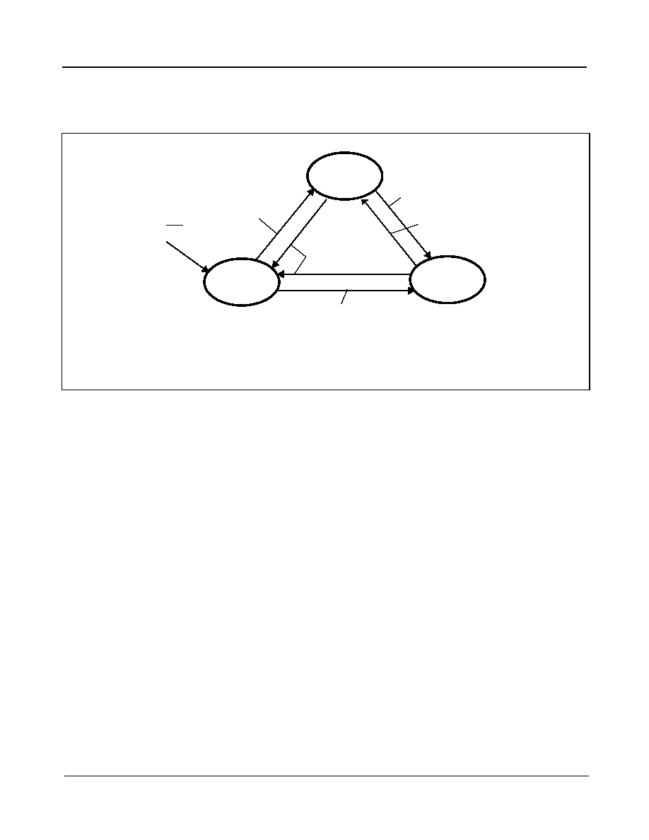
3.4 Digital Phase Lock Loop (DPLL)
The DPLL of the ZL30102 consists of a phase detector, a limiter, a loop filter and a digitally controlled oscillator as
shown in Figure 10. The data path from the phase detector to the limiter is tapped and routed to the lock detector
that provides a lock indication which is output at the LOCK pin.
Figure 10 - DPLL Block Diagram
Phase Detector - the phase detector compares the virtual reference signal from the TIE corrector circuit with the
feedback signal and provides an error signal corresponding to the phase difference between the two. This error
signal is passed to the limiter circuit.
Limiter - the limiter receives the error signal from the phase detector and ensures that the DPLL responds to all
input transient conditions with a maximum output phase slope compliant with the applicable standards. The phase
slope limit is dependent on the SEC_MSTR pin and is listed in Table 2.
Loop Filter - the loop filter is similar to a first order low pass filter with a bandwidth of 1.8 Hz suitable to provide
Primary Master timing. When Secondary Master mode is selected (SEC_MSTR=1), the filter bandwidth is set to
922 Hz. For stability reasons, the loop filter bandwidth for 8 kHz reference inputs is limited to a maximum of 58 Hz.
State Select from
Control State Machine
Feedback signal from
Frequency Select MUX
DPLL Reference to
Frequency Synthesizer
Virtual Reference
from
TIE Corrector Circuit
Limiter
Loop Filter
Digitally
Controlled
Oscillator
Phase
Detector
REF2_SYNC
frame pulse
Lock
detector
LOCK
feedback frame pulse; F8o or F2ko

ZL30102
Data Sheet
20
Zarlink Semiconductor Inc.
Digitally Controlled Oscillator (DCO) - the DCO receives the limited and filtered signal from the Loop Filter, and
based on its value, generates a corresponding digital output signal. The synchronization method of the DCO is
dependent on the state of the ZL30102.
In Normal Mode, the DCO provides an output signal which is frequency and phase locked to the selected input
reference signal.
In Holdover Mode, the DCO is free running at a frequency equal to the frequency that the DCO was generating in
Normal Mode. The frequency in Holdover mode is calculated from frequency samples stored 26 ms to 52 ms before
the ZL30102 entered Holdover mode. This ensures that the coarse frequency monitor and the single cycle monitor
have time to disqualify a bad reference before it corrupts the holdover frequency.
In Freerun Mode, the DCO is free running with an accuracy equal to the accuracy of the OSCi 20 MHz source.
Lock Indicator - the lock detector monitors if the output value of the phase detector is within the phase-lock-
window for a certain time. The selected phase-lock-window guarantees the stable operation of the LOCK pin with
maximum network jitter and wander on the reference input. If the DPLL goes into Holdover mode (auto or manual),
the LOCK pin will initially stay high for 1 s in Primary Master mode. In Secondary Master mode, LOCK remains high
for 0.1 s. If at that point the DPLL is still in holdover mode, the LOCK pin will go low; subsequently the LOCK pin will
not return high for at least the full lock-time duration. In Freerun mode the LOCK pin will go low immediately.
3.5 Frequency Synthesizers
The output of the DCO is used by the frequency synthesizers to generate the output clocks and frame pulses which
are synchronized to one of three reference inputs (REF0, REF1 or REF2). The frequency synthesizer uses digital
techniques to generate output clocks and advanced noise shaping techniques to minimize the output jitter. The
clock and frame pulse outputs have limited driving capability and should be buffered when driving high capacitance
loads.
3.6 State Machine
As shown in Figure 1, the state machine controls the TIE Corrector Circuit and the DPLL. The control of the
ZL30102 is based on the inputs MODE_SEL1:0, REF_SEL1:0 and HMS.
3.7 Master Clock
The ZL30102 can use either a clock or crystal as the master timing source. For recommended master timing
circuits, see the Applications - Master Clock section.

ZL30102
Data Sheet
21
Zarlink Semiconductor Inc.
4.0 Control and Modes of Operation
4.1 Out of Range Selection
The out of range limits for the Precise Frequency Monitor in the 3 reference monitor blocks are selected through the
OOR_SEL pin, see Table 1.
4.2 Loop Filter and Limiter Selection
The loop filter and limiter settings are selected through the SEC_MSTR pin, see Table 2. The maximum loop filter
bandwidth is also dependent on the frequency of the currently selected reference (REF0/1/2).
4.3 Output Clock and Frame Pulse Selection
The output of the DCO is used by the frequency synthesizers to generate the output clocks and frame pulses which
are synchronized to one of three reference inputs (REF0, REF1 or REF2). These signals are available in two
groups controlled by the OUT_SEL pin, see Table 3.
4.4 Modes of Operation
The ZL30102 has three possible manual modes of operation; Normal, Holdover and Freerun. These modes are
selected with mode select pins MODE_SEL1 and MODE_SEL0 as is shown in Table 4. Transitioning from one
mode to the other is controlled by an external controller. The ZL30102 can be configured to automatically select a
valid input reference under control of its internal state machine by setting MODE_SEL1:0 = 11. In this mode of
operation, a state machine controls selection of references (REF0 or REF1) used for synchronization.
OOR_SEL
Application
Applicable Standard
Out Of Range Limits
0
DS1
ANSI T1.403
Telcordia GR-1244-CORE Stratum 4/4E
64 - 83 ppm
1
E1
ITU-T G.703
ETSI ETS 300 011
100 - 130 ppm
Table 1 - Out of Range Limits Selection
SEC_MSTR
Detected REF Frequency
Loop Filter Bandwidth
Phase Slope Limiting
0
any
1.8 Hz
61
�/s
1
8 kHz
58 Hz
9.5 ms /s
1.544 MHz, 2.048 MHz,
8.192 MHz, 16.384 MHz
922 Hz
9.5 ms /s
Table 2 - Loop Filter and Limiter Settings
OUT_SEL
Generated Clocks
Generated Frame Pulses
0
C2o, C4o, C8o, C16o
F4o, F8o, F16o
1
C2o, C16o, C32, C65o
F16o, F32o, F65o
Table 3 - Clock and Frame Pulse Selection with OUT_SEL Pin

ZL30102
Data Sheet
22
Zarlink Semiconductor Inc.
4.4.1 Freerun Mode
Freerun mode is typically used when an independent clock source is required, or immediately following system
power-up before network synchronization is achieved.
In Freerun mode, the ZL30102 provides timing and synchronization signals which are based on the master clock
frequency (supplied to OSCi pin) only, and are not synchronized to the reference input signals.
The accuracy of the output clock is equal to the accuracy of the master clock (OSCi). So if a
�
32 ppm output clock
is required, the master clock must also be
�
32 ppm. See Applications - Section 6.2, "Master Clock".
4.4.2 Holdover Mode
Holdover Mode is typically used for short durations while network synchronization is temporarily disrupted.
In Holdover Mode, the ZL30102 provides timing and synchronization signals, which are not locked to an external
reference signal, but are based on storage techniques. The storage value is determined while the device is in
Normal Mode and locked to an external reference signal.
When in Normal Mode, and locked to the input reference signal, a numerical value corresponding to the ZL30102
output reference frequency is stored alternately in two memory locations every 26 ms. When the device is switched
into Holdover Mode, the value in memory from between 26 ms and 52 ms is used to set the output frequency of the
device. The frequency accuracy of Holdover Mode is 0.1 ppm.
Two factors affect the accuracy of Holdover mode. One is drift on the master clock while in Holdover mode, drift on
the master clock directly affects the Holdover mode accuracy. Note that the absolute master clock (OSCi) accuracy
does not affect Holdover accuracy, only the change in OSCi accuracy while in Holdover. For example, a
�
32 ppm
master clock may have a temperature coefficient of
�
0.1 ppm per �C. So a
�
10 �C change in temperature, while the
ZL30102 is in Holdover mode may result in an additional offset (over the 0.1 ppm) in frequency accuracy of
�
1 ppm. Which is much greater than the 0.1 ppm of the ZL30102. The other factor affecting the accuracy is large
jitter on the reference input prior to the mode switch.
MODE_SEL1
MODE_SEL0
Mode
0
0
Normal (with automatic Holdover)
0
1
Holdover
1
0
Freerun
1
1
Automatic
(Normal with automatic Holdover and
automatic reference switching)
Table 4 - Operating Modes
ZL30102
Data Sheet
23
Zarlink Semiconductor Inc.
4.4.3 Normal Mode
Normal mode is typically used when a system clock source, synchronized to the network is required. In Normal
mode, the ZL30102 provides timing (C1.5o, C2o, C4o, C8o, C16o, C19o, C32 and C65o) and frame
synchronization (F2ko, F4o, F8o, F16o, F32o and F65o) signals, which are synchronized to one of three reference
inputs (REF0, REF1 or REF2). The input reference signal may have a nominal frequency of 8 kHz, 1.544 MHz,
2.048 MHz, 8.192 MHz or 16.384 MHz. The frequency of the reference inputs are automatically detected by the
reference monitors.
When the ZL30102 comes out of RESET while Normal mode is selected by its MODE_SEL pins then it will initially
go into Holdover mode and generate clocks with the accuracy of its freerunning local oscillator (see Figure 11). If
the ZL30102 determines that its selected reference is disrupted (see Figure 3), it will remain in Holdover until the
selected reference is no longer disrupted or the external controller selects another reference that is not disrupted. If
the ZL30102 determines that its selected reference is not disrupted (see Figure 3) then the state machine will cause
the DPLL to recover from Holdover via one of two paths depending on the logic level at the HMS pin. If HMS=0 then
the ZL30102 will transition directly to Normal mode and it will align its output signals with its selected input
reference (see Figure 9). If HMS=1 then the ZL30102 will transition to Normal mode via the TIE correction state and
the phase difference between the output signals and the selected input reference will be maintained.
When the ZL30102 is operating in Normal mode, if it determines that its selected reference is disrupted (Figure 3)
then its state machine will cause it to automatically go to Holdover mode. When the ZL30102 determines that its
selected reference is not disrupted then the state machine will cause the DPLL to recover from Holdover via one of
two paths depending on the logic level at the HMS pin (see Figure 11). If HMS=0 then the ZL30102 will transition
directly to Normal mode and it will align its output signals with its input reference (see Figure 9). If HMS=1 then the
ZL30102 will transition to Normal mode via the TIE correction state and the phase difference between the output
signals and the input reference will be maintained.
If the reference selection changes because the value of the REF_SEL1:0 pins changes or because the reference
selection state machine selected a different reference input, the ZL30102 goes into Holdover mode and returns to
Normal mode through the TIE correction state regardless of the logic value on HMS pin.
ZL30102 provides a fast lock pin (FASTLOCK), which, when set high enables the PLL to lock to an incoming
reference within approximately 1 s.
Figure 11 - Mode Switching in Normal Mode
REF_DIS=1: Current selected reference disrupted (see Figure 3). REF_DIS is an internal signal.
REF_CH= 1: Reference change, a transition in the reference selection (see Figure 13) or a change in the
REF_SEL pins. REF_CH is an internal signal.
TIE Correction
(HOLDOVER=1)
Holdover
(HOLDOVER=1)
REF_DIS=0
REF_CH=1
REF_DIS=0 and
REF_DIS=1
(REF_DIS=0 and HMS=1) or
REF_CH=1
REF_DIS=1
RST
REF_CH=0 and
HMS=0
Normal
(HOLDOVER=0)
ZL30102
Data Sheet
24
Zarlink Semiconductor Inc.
4.4.4 Automatic Mode
The Automatic mode combines the functionality of the Normal mode (automatic Holdover) with automatic reference
switching. The automatic reference switching is described in more detail in section 4.5.2, "Automatic Reference
Switching".
4.5 Reference Switching
4.5.1 Manual Reference Switching
In the manual modes of operation (MODE_SEL1:0
11) the active reference input (REF0, REF1 or REF2) is
selected by the REF_SEL1 and REF_SEL0 pins as shown in Table 5. When the logic value of the REF_SEL pins is
changed when the DPLL is in Normal mode, the ZL30102 will perform a hitless reference switch.
When the REF_SEL inputs are used in Normal mode to force a change from the currently selected reference to
another reference, the action of the LOCK output will depend on the relative frequency and phase offset of the old
and new references. Where the new reference has enough frequency offset and/or TIE-corrected phase offset to
force the output outside the phase-lock-window, the LOCK output will de-assert, the lock-qualify timer is reset, and
LOCK will stay de-asserted for the full lock-time duration. Where the new reference is close enough in frequency
and TIE-corrected phase for the output to stay within the phase-lock-window, the LOCK output will remain asserted
through the reference-switch process.
Figure 12 - Reference Switching in Normal Mode
REF_SEL1
REF_SEL0
Input Reference Selected
0
0
REF0
0
1
REF1
1
0
REF2
1
1
REF2
Table 5 - Manual Reference Selection
REF1
REF0
REF_SEL
LOCK
Lock Time
Note: LOCK pin behaviour depends on phase and frequency offset of REF1.
ZL30102
Data Sheet
25
Zarlink Semiconductor Inc.
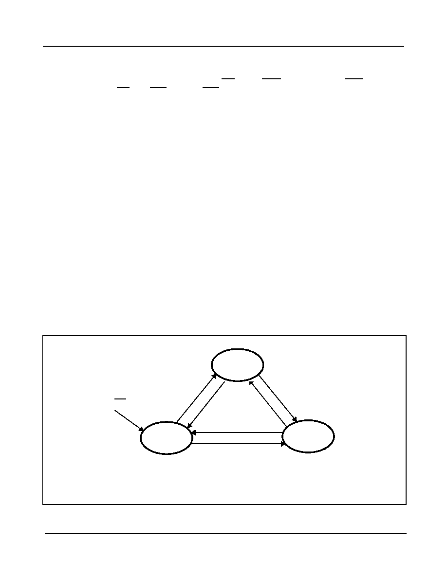
4.5.2 Automatic Reference Switching
In the automatic mode of operation (MODE_SEL1:0
= 11), the ZL30102 automatically selects a reference input that
is not out-of-range (REF_OOR=0, see Figure 3). The state machine can only select REF0 or REF1; REF2 cannot
be selected in the Automatic mode (see Figure 13).
If the current reference (REF0 or REF1) used for synchronization fails, the state machine will switch to the other
reference. If both references fail then the ZL30102 enters the Holdover mode without switching to another
reference. When the ZL30102 comes out of reset or when REF2 is the current reference when the ZL30102 is put
in the Automatic mode, then REF0 has priority over REF1. Otherwise there is no preference for REF0 or REF1
which is referred to as non-revertive reference selection.
Figure 13 - Reference Selection in Automatic Mode (MODE_SEL=11)
In the automatic mode of operation, both pins REF_SEL1 and REF_SEL0 are configured as outputs. The logic level
on the REF_SEL0 output indicates the current input reference being selected for synchronization (see Table 6).
REF_SEL1
(output pin)
REF_SEL0
(output pin)
Input Reference
0
0
REF0
0
1
REF1
Table 6 - The Reference Selection Pins in the Automatic Mode (MODE_SEL=11)
REF0
Reference
REF1
Reference
REF_OOR0=1 &&
REF_OOR1=0
RST && REF_OOR0=0
RST && REF_OOR0=1 && REF_OOR1=0
REF_OOR0=0 &&
REF_OOR1=1
REF2
Reference
REF_OOR0=1 && REF_OOR1=0
REF_OOR0=0
REF_OOR = reference out of range, see Figure 3.
This is an internal signal.
ZL30102
Data Sheet
26
Zarlink Semiconductor Inc.
The mode selection state machine behaves differently in Automatic mode in that when both reference REF0 and
reference REF1 are out of range (REF_OOR=1), the state machine will select the Holdover state. In Normal mode
the reference out of range (REF_OOR) status is ignored by the state machine. This is illustrated in Figure 14.
Figure 14 - Mode Switching in Automatic Mode
4.5.2.1 Automatic Reference Switching - Coarse Reference Failure
When the currently-active input reference in Automatic mode fails in a coarse manner, the REF_DIS internal signal
places the device in holdover, with the HOLDOVER pin and the REF_FAIL pin asserted. This can occur through
triggering the Single Cycle Monitor, or the Coarse Frequency Monitor, in the Reference Monitor block. If the
reference does not correct itself within the lock-disqualify duration (1 second) the LOCK pin is de-asserted. If the
reference does not correct itself within the reference-disqualify duration (2.5 seconds) the HOLDOVER pin is de-
asserted and the REF_SEL outputs indicate that the device has switched to the other reference. The LOCK pin
remains de-asserted for the full lock-time duration, regardless of the phase and frequency offset of the old and new
references. Figure 15 illustrates this process.
If the reference corrects itself within the lock-disqualify duration (< 1 second) the HOLDOVER pin is de-asserted,
and the REF_FAIL pin is de-asserted. The LOCK pin remains asserted. No reference switching takes place, and
the REF_SEL outputs indicate that the device has remained locked to the old reference.
If the reference does not correct itself within the lock-disqualify duration (1 second), but does correct itself within the
reference-disqualify duration (< 2.5 seconds) the HOLDOVER pin is de-asserted, the REF_FAIL pin is de-asserted,
and the REF_SEL outputs indicate that the device has remained locked to the old reference. However the LOCK
pin is de-asserted, the lock-qualify timer is reset, and the LOCK pin remains de-asserted for the full lock-time
duration. See 7.2, "Performance Characteristics" on page 46 for lock-time duration.
REF_DIS=1: Current selected reference disrupted (see Figure 3). REF_DIS is an internal signal.
REF_OOR=1: Current selected reference out of range (see Figure 3). REF_OOR is an internal signal.
REF_CH= 1: Reference change, a transition in the reference selection (see Figure 13). REF_CH is an internal signal.
TIE Correction
(HOLDOVER=1)
Holdover
(HOLDOVER=1)
REF_DIS=0
REF_CH=1
REF_DIS=1
(REF_DIS=0 and REF_OOR=0 and HMS=1)
RST
Normal
(HOLDOVER=0)
and REF_OOR=0
or REF_OOR=1
or REF_CH=1
REF_DIS=0 and REF_OOR=0
and REF_CH=0 and HMS=0

ZL30102
Data Sheet
27
Zarlink Semiconductor Inc.
Figure 15 - Automatic Reference Switching - Coarse Reference Failure
4.5.2.2 Automatic Reference Switching - Reference Frequency Out-of-Range
When the currently-active input reference in Automatic mode fails through a subtle frequency offset, the REF_FAIL
output is asserted as soon as the Precise Frequency Monitor indicates an out-of-range reference (10 to 20
seconds). The HOLDOVER output is briefly asserted (approximately three reference input cycles) and the
REF_SEL outputs indicate that the device has switched to the other reference. Where the new reference is close
enough in frequency and TIE-corrected phase for the output to stay within the phase-lock-window, the LOCK output
will remain asserted through the reference-switch process. Where the new reference has enough frequency offset
and/or TIE-corrected phase offset to force the output outside the phase-lock-window, the LOCK output will de-
assert, the lock-qualify timer is reset, and LOCK will stay de-asserted for the full lock-time duration. Figure 16
illustrates this process.
2.5 s
10 s
REF0
REF_FAIL0
HOLDOVER
REF_OOR0
(internal signal)
REF1
REF0
REF_SEL
SCM or CFM failure
LOCK
1 s
Lock Time
REF_DIS0
(internal signal)
Note: this scenario is based on REF1 remaining good throughout the duration.
ZL30102
Data Sheet
28
Zarlink Semiconductor Inc.
Figure 16 - Automatic Reference Switching - Out-of-Range Reference Failure
4.6 Clock Redundancy Support
In general, clock redundancy implies that the redundant timing card DPLL tracks the output clock and/or frame
pulse of the active timing card DPLL. In case that the active timing card fails, the devices that use the active clock
and/or frame pulse must be able to switch to the redundant clock and/or frame pulse without experiencing
disruptions. Therefore the redundant signals must closely track the active signals. The ZL30102 supports this kind
of clock redundancy in various ways;
� Lock only to the active clock. The ZL30102 uses the 922 Hz loop filter bandwidth to closely track the active
clock, even in the presence of jitter on the active clock. However the active and redundant frame pulse may
not be aligned.
� Lock to the active frame pulse. Both the redundant clock and frame pulse will be aligned with the active clock
and frame pulse. However the ZL30102 loop filter bandwidth is limited to 58 Hz for an 8 kHz frame pulse.
Therefore the redundant clock and frame pulse will not track the active frame pulse as closely in the
presence of jitter on the active frame pulse as with a 922 Hz loop filter bandwidth.
� Lock to both the active clock and associated frame pulse. The ZL30102 uses the 922 Hz loop filter
bandwidth and thereby track the active clock and frame pulse in the presence of jitter on the active signals. It
will also align the redundant frame pulse with the active frame pulse.
The method of clock redundancy shown in Figure 18 is that the redundant timing card is frequency and phase
locked to the active clock and frame pulse. The redundant card is configured as Secondary Master (SEC_MSTR=1)
and continuously adjusts the phase of its output clocks and frame pulses to match that of the active clock and frame
pulse. In this mode of operation, the bandwidth of the redundant timing card's DPLL is much larger than that of the
active timing card's DPLL, 922 Hz versus 1.8 Hz. Therefore the redundant clocks and frame pulses will track the
10 to 20 s
REF0
REF_FAIL0
HOLDOVER
REF_OOR0
(internal signal)
REF1
REF0
REF_SEL
Frequency Precision failure
LOCK
Note: This scenario is based on REF1 remaining good throughout the duration.
Lock Time
LOCK pin behaviour depends on phase and frequency offset of REF1.
ZL30102
Data Sheet
29
Zarlink Semiconductor Inc.
active clock and frame pulse closely even in the presence of the maximum tolerable input jitter and wander on the
active timing card's reference input.
The method of synchronization using REF2 and REF2_SYNC is enabled as soon as a valid 8 kHz frame pulse is
detected on the REF2_SYNC input. The REF2_SYNC pulse must be generated from the clock that is present on
the REF2 input. The ZL30102 checks the number of REF2 cycles in the REF2_SYNC period. If this is not the
nominal number of cycles, the REF2_SYNC pulse is considered invalid. For example, if REF2 is a 8.192 MHz clock
and REF2_SYNC is a 8 kHz frame pulse, then there must be exactly 1024 REF2 cycles in a REF2_SYNC period. If
a valid REF2_SYNC pulse is detected, the ZL30102 will align the rising edges of the REF2 clock and the
corresponding output clock such that the rising edge of the F8o/F32o output frame pulse is aligned with the frame
boundary indicated by the REF2_SYNC signal. The rising edges of the REF2 and the corresponding output clock
that are aligned, are the ones that lag the rising edges of the REF2_SYNC and the F8o pulses respectively. This is
illustrated in Figure 17. Many combinations of the ZL30102 clock and frame pulse outputs can be used as REF2
and REF2_SYNC inputs. In general, the active low frame pulses F4o, F16o and F65o would be inverted first before
used as a REF2_SYNC input.
Figure 17 - Examples of REF2 & REF2_SYNC to Output Alignment
REF2 = C8o
REF2_SYNC = 8 kHz
F8o
aligned
C8o
ZL30102
Data Sheet
30
Zarlink Semiconductor Inc.
Figure 18 - Clock Redundancy with Two Independent Timing Cards
The following is an example of how active/redundant setup can be configured.
The active timing card is set based on the desired application and is set to:
� Primary master mode, SEC_MSTR=0
� Normal Mode, MODE_SEL1:0=00 (forces device to the input reference set at REF_SEL)
� Automatic mode, MODE_SEL1:0=11 (allows device to auto-switch if reference fails)
The HOLDOVER and REF_FAIL pins help evaluate quality of clocks and quality of redundant clock.
The redundant timing card is set based on desired applications and is set to:
� Normal (manual) mode, MODE_SEL1:0=00
� REF2 and REF2_SYNC as the input reference, REF_SEL1=1 (forces redundant device to lock to output
of active card)
� Secondary master mode, SEC_MSTR=1
The HOLDOVER and REF_FAIL pins help evaluate quality of clocks and quality of redundant clock.
Active Timing Card
OSC
ZL30102
BITS 0 clock
BITS 1 clock
Output Clocks
Redundant Timing Card
OSC
ZL30102
Output Clocks
Active Clock
Redundant Clock
REF0
REF1
REF2
REF2_SYNC
REF2
REF2_SYNC
Active Frame Sync (optional)
Redundant Frame Sync (optional)
MODE_SEL1:0=00
REF_SEL1:0=10
SEC_MSTR=1
MODE_SEL1:0=11
SEC_MSTR=0
BITS 0 clock
BITS 1 clock
REF0
REF1

ZL30102
Data Sheet
31
Zarlink Semiconductor Inc.
When the redundant timing card is switched to becoming the active timing card, the system controller should do the
following:
� select Primary Master mode, SEC_MSTR=0
� select Automatic mode, MODE_SEL1:0=11
The new active timing card will automatically select a valid input reference REF0 or REF1. If both input references
are available and valid, then REF0 will be chosen over REF1. If the new active timing card should use the same
input reference (REF0 or REF1) as the old active timing card used before it failed, The system controller should do
the following instead:
� select Holdover (manual) mode, MODE_SEL1:0=01
� select Primary Master mode, SEC_MSTR=0
� select the required reference (REF0 or REF1) as the input reference
� Normal Mode, MODE_SEL1:0=00 (forces device to the input reference set at REF_SEL)
� select Automatic mode, MODE_SEL1:0=11
It is recommended to maintain HMS=1 when switching from redundant to active through the Holdover mode, to
eliminate output phase transients.
When the active timing card is switched to becoming the redundant timing card, the system controller should do the
following:
� select Normal (manual) mode, MODE_SEL1:0=00
� select Secondary Master mode, SEC_MSTR=1
� select REF2 and REF2_SYNC as the input reference, REF_SEL1=1
The ZL30102 allows for the switch from Secondary Master mode to Primary Master mode with no frequency or
phase hits on the output clocks. The switch from Primary Master mode to Secondary Master mode may introduce a
phase transient on the output clocks as the TIE correction circuit is disabled to allow the Secondary master device
to track the active clocks closely.

ZL30102
Data Sheet
32
Zarlink Semiconductor Inc.
5.0 Measures of Performance
The following are some PLL performance indicators and their corresponding definitions.
5.1 Jitter
Timing jitter is defined as the high frequency variation of the clock edges from their ideal positions in time. Wander
is defined as the low-frequency variation of the clock edges from their ideal positions in time. High and low
frequency variation imply phase oscillation frequencies relative to some demarcation frequency. (Often 10 Hz or
20 Hz for DS1 or E1, higher for SONET/SDH clocks.) Jitter parameters given in this data sheet are total timing jitter
numbers, not cycle-to-cycle jitter.
5.2 Jitter Generation (Intrinsic Jitter)
Jitter generation is the measure of the jitter produced by the PLL and is measured at its output. It is measured by
applying a reference signal with no jitter to the input of the device, and measuring its output jitter. Jitter generation
may also be measured when the device is in a non-synchronizing mode, such as free running or holdover, by
measuring the output jitter of the device. Jitter is usually measured with various bandlimiting filters depending on
the applicable standards.
5.3 Jitter Tolerance
Jitter tolerance is a measure of the ability of a PLL to operate properly (i.e., remain in lock and or regain lock in the
presence of large jitter magnitudes at various jitter frequencies) when jitter is applied to its reference. The applied
jitter magnitude and jitter frequency depends on the applicable standards.
5.4 Jitter Transfer
Jitter transfer or jitter attenuation refers to the magnitude of jitter at the output of a device for a given amount of jitter
at the input of the device. Input jitter is applied at various amplitudes and frequencies, and output jitter is measured
with various filters depending on the applicable standards.
For the Zarlink digital PLLs two internal elements determine the jitter attenuation; the internal low pass loop filter
and the phase slope limiter. The phase slope limiter limits the output phase slope to, for example, 61
�s/s.
Therefore, if the input signal exceeds this rate, such as for very large amplitude low frequency input jitter, the
maximum output phase slope will be limited (i.e., attenuated).
Since intrinsic jitter is always present, jitter attenuation will appear to be lower for small input jitter signals than for
large ones. Consequently, accurate jitter transfer function measurements are usually made with large input jitter
signals (for example 75% of the specified maximum tolerable input jitter).
5.5 Frequency Accuracy
The Frequency accuracy is defined as the absolute accuracy of an output clock signal when it is not locked to an
external reference, but is operating in a free running mode.
5.6 Holdover Accuracy
Holdover accuracy is defined as the absolute accuracy of an output clock signal, when it is not locked to an external
reference signal, but is operating using storage techniques. For the ZL30102, the storage value is determined while
the device is in Normal Mode and locked to an external reference signal.

ZL30102
Data Sheet
33
Zarlink Semiconductor Inc.
5.7
Pull-in
Range
Also referred to as capture range. This is the input frequency range over which the PLL must be able to pull into
synchronization.
5.8 Lock Range
This is the input frequency range over which the synchronizer must be able to maintain synchronization.
5.9 Phase Slope
Phase slope is measured in seconds per second and is the rate at which a given signal changes phase with respect
to an ideal signal. The given signal is typically the output signal. The ideal signal is of constant frequency and is
nominally equal to the value of the final output signal or final input signal. Another way of specifying the phase slope
is as the fractional change per time unit. For example; a phase slope of 61
�s/s can also be specified as 61 ppm.
5.10 Time Interval Error (TIE)
TIE is the time delay between a given timing signal and an ideal timing signal.
5.11 Maximum Time Interval Error (MTIE)
MTIE is the maximum peak to peak delay between a given timing signal and an ideal timing signal within a
particular observation period.
5.12 Phase Continuity
Phase continuity is the phase difference between a given timing signal and an ideal timing signal at the end of a
particular observation period. Usually, the given timing signal and the ideal timing signal are of the same frequency.
Phase continuity applies to the output of the PLL after a signal disturbance due to a reference switch or a mode
change. The observation period is usually the time from the disturbance, to just after the synchronizer has settled to
a steady state.
5.13 Lock Time
This is the time it takes the PLL to frequency lock to the input signal. Phase lock occurs when the input signal and
output signal are aligned in phase with respect to each other within a certain phase distance (not including jitter).
Lock time is affected by many factors which include:
� initial input to output phase difference
� initial input to output frequency difference
� PLL loop filter bandwidth
� PLL phase slope limiter
� in-lock phase distance
The presence of input jitter makes it difficult to define when the PLL is locked as it may not be able to align its output
to the input within the required phase distance, dependent on the PLL bandwidth and the input jitter amplitude and
frequency.
Although a short lock time is desirable, it is not always possible to achieve due to other synchronizer requirements.
For instance, better jitter transfer performance is achieved with a lower frequency loop filter which increases lock
time. And better (smaller) phase slope performance (limiter) results in longer lock times.

ZL30102
Data Sheet
34
Zarlink Semiconductor Inc.
6.0 Applications
This section contains ZL30102 application specific details for power supply decoupling, reset operation, clock and
crystal operation.
6.1 Power Supply Decoupling
It is recommended to place a 100 nF decoupling capacitor close to each pair of power and ground pins as
illustrated in Figure 19 to ensure optimal jitter performance.
Figure 19 - Recommended Power Supply Decoupling
6.2 Master Clock
The ZL30102 can use either a clock or crystal as the master timing source. Zarlink application note ZLAN-68 lists a
number of applicable oscillators and crystals that can be used with the ZL30102.
100 nF
33
AGND
36
AVDD
25
V
DD
61
V
DD
37
AV
DD
V
CORE
12
AV
CORE
35
GND
1
AV
CORE
14
1.8 V
3.3 V
44
AV
DD
45
AV
DD
100 nF
100 nF
100 nF
29
AV
DD
41
AGND
51
AGND
23
GND
ZL30102
100 nF
100 nF
GND
13
V
CORE
2
100 nF
1
GND
100 nF
100 nF
40
GND
34
GND
100 nF
100 nF
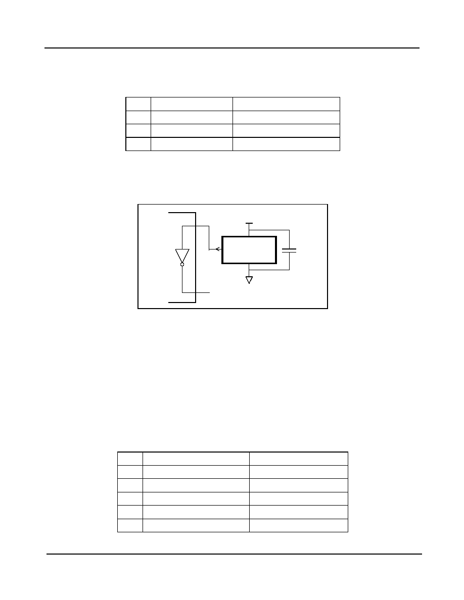
ZL30102
Data Sheet
35
Zarlink Semiconductor Inc.
6.2.1 Clock Oscillator
When selecting a clock oscillator, numerous parameters must be considered. This includes absolute frequency,
frequency change over temperature, output rise and fall times, output levels, duty cycle and phase noise.
The output clock should be connected directly (not AC coupled) to the OSCi input of the ZL30102, and the OSCo
output should be left open as shown in Figure 20.
Figure 20 - Clock Oscillator Circuit
6.2.2 Crystal Oscillator
Alternatively, a Crystal Oscillator may be used. A complete oscillator circuit made up of a crystal, resistor and
capacitors is shown in Figure 21.
The accuracy of a crystal oscillator depends on the crystal tolerance as well as the load capacitance tolerance.
Typically, for a 20 MHz crystal specified with a 32 pF load capacitance, each 1 pF change in load capacitance
contributes approximately 9 ppm to the frequency deviation. Consequently, capacitor tolerances and stray
capacitances have a major effect on the accuracy of the oscillator frequency.
The crystal should be a fundamental mode type - not an overtone. The fundamental mode crystal permits a simpler
oscillator circuit with no additional filter components and is less likely to generate spurious responses. A typical
crystal oscillator specification and circuit is shown in Table 8 and Figure 21 respectively.
.
1
Frequency
20 MHz
2
Tolerance
as required
3
Rise & fall time
< 10 ns
4
Duty cycle
40% to 60%
Table 7 - Typical Clock Oscillator Specification
1
Frequency
20 MHz
2
Tolerance
as required
3
Oscillation mode
fundamental
4
Resonance mode
parallel
5
Load capacitance
as required
6
Maximum series resistance
50
Table 8 - Typical Crystal Oscillator Specification
+3.3 V
20 MHz OUT
GND
0.1 �F
+3.3 V
OSCo
ZL30102
OSCi
No Connection

ZL30102
Data Sheet
36
Zarlink Semiconductor Inc.
Figure 21 - Crystal Oscillator Circuit
6.3 Power Up Sequence
The ZL30102 requires that the 3.3 V supply is not powered up after the 1.8 V supply. This is to prevent the risk of
latch-up due to the presence of parasitic diodes in the IO pads.
Two options are given:
1. Power-up the 3.3 V supply fully first, then power up the 1.8 V supply
2. Power up the 3.3 V supply and the 1.8 V supply simultaneously, ensuring that the 3.3 V supply is never lower
than a few hundred millivolts below the 1.8 V supply (e.g., by using a schottky diode or controlled slew rate)
6.4 Reset Circuit
A simple power up reset circuit with about a 60
�s reset low time is shown in Figure 22. Resistor R
P
is for protection
only and limits current into the RST pin during power down conditions. The reset low time is not critical but should
be greater than 300 ns.
Figure 22 - Power-Up Reset Circuit
OSCo
1 M
20 MHz
ZL30102
OSCi
100
1
�H
The 100
resistor and the 1 �H inductor may improve
stability and are optional.
+3.3 V
RST
R
P
1 k
C
10 nF
R
10 k
ZL30102
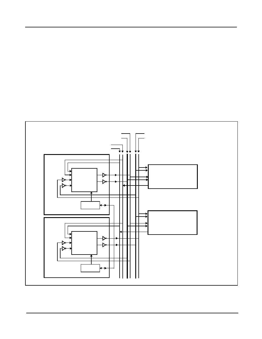
ZL30102
Data Sheet
37
Zarlink Semiconductor Inc.
6.5 Clock Redundancy System Architecture
Carrier-Class Telecommunications Equipment deployed in today's networks guarantee better than 99.999%
operational availability (equivalent to less than 7 minutes of downtime per year). This high level of uninterrupted
service is achieved by fully redundant architectures with hot swappable cards like an ECTF H.110 compliant
system. Timing for these types of systems can be generated by the ZL30102 which supports primary/secondary
master timing protection switching.
The architecture shown in Figure 23 is based on the ZL30102 being deployed on two separate timing cards; the
primary master timing card and the secondary master timing card. In normal operation the primary master timing
card receives synchronization from the network and provides timing for the whole system. The redundant
secondary master timing card is phase locked to the backplane clock and frame pulse through its REF2 and
REF2_SYNC inputs. These two designated inputs allow the secondary master timing card to track the primary
master timing card clocks with minimal phase skew. When the primary master timing card fails unexpectedly (this
failure is not related to reference failure) then all switch cards or line cards will detect this failure and they will switch
to the timing supplied by the secondary master timing card. The secondary master timing card will be promoted to
primary master and switch from using the REF2 and REF2_SYNC inputs to one of the REF0 or REF1 inputs.
Figure 23 - Typical Clocking Architecture of an ECTF H.110 System
ZL30102
REF2
REF0
Primary Master Timing Card
REF1
Backplane
REF2_SYNC
C8o
F8o
CT_C8_A
CT_FRAME_A
CT_C8_B
CT_FRAME_B
CT_NETREF_1
CT_NETREF_2
SEC_MSTR
Master/Slave
Control
0
ZL30102
REF2
REF0
Secondary Master Timing Card
REF1
REF2_SYNC
C8o
F8o
SEC_MSTR
Master/Slave
Control
1
Switch Card or Line Card
Switch Card or Line Card

ZL30102
Data Sheet
38
Zarlink Semiconductor Inc.
7.0 Characteristics
7.1 AC and DC Electrical Characteristics
* Exceeding these values may cause permanent damage. Functional operation under these conditions is not implied.
* Voltages are with respect to ground (GND) unless otherwise stated.
* Voltages are with respect to ground (GND) unless otherwise stated.
Absolute Maximum Ratings*
Parameter
Symbol
Min.
Max.
Units
1
Supply voltage
V
DD_R
-0.5
4.6
V
2
Core supply voltage
V
CORE_R
-0.5
2.5
V
3
Voltage on any digital pin
V
PIN
-0.5
6
V
4
Voltage on OSCi and OSCo pin
V
OSC
-0.3
V
DD
+ 0.3
V
5
Current on any pin
I
PIN
30
mA
6
Storage temperature
T
ST
-55
125
�C
7
TQFP 64 pin package power dissipation
P
PD
500
mW
8
ESD rating
V
ESD
2
kV
Recommended Operating Conditions*
Characteristics
Sym.
Min.
Typ.
Max.
Units
1
Supply voltage
V
DD
2.97
3.30
3.63
V
2
Core supply voltage
V
CORE
1.62
1.80
1.98
V
3
Operating temperature
T
A
-40
25
85
�C
DC Electrical Characteristics*
Characteristics
Sym.
Min.
Max.
Units
Notes
1
Supply current with: OSCi = 0 V
I
DDS
1
9
mA
outputs loaded
with 30 pF
2
OSCi = Clock, OUT_SEL=0
I
DD
30
60
mA
3
OSCi = Clock, OUT_SEL=1
I
DD
41
73
mA
4
Core supply current with: OSCi = 0 V
I
CORES
0
30
�A
5
OSCi = Clock
I
CORE
14
20
mA
6
Schmitt trigger Low to High threshold
point
V
t+
1.47
1.5
V
All device inputs are
Schmitt trigger type.
7
Schmitt trigger High to Low threshold
point
V
t-
0.80
1.0
V
8
Input leakage current
I
IL
-105
105
�A
V
I
= V
DD
or 0 V
9
High-level output voltage
V
OH
2.4
V
I
OH
= 8 mA for clock and
frame-pulse outputs,
4 mA for status outputs

ZL30102
Data Sheet
39
Zarlink Semiconductor Inc.
* Supply voltage and operating temperature are as per Recommended Operating Conditions.
* Voltages are with respect to ground (GND) unless otherwise stated.
* Supply voltage and operating temperature are as per Recommended Operating Conditions.
* Voltages are with respect to ground (GND) unless otherwise stated.
Figure 24 - Timing Parameter Measurement Voltage Levels
* Supply voltage and operating temperature are as per Recommended Operating Conditions.
* Period Min/Max values are the limits to avoid a single-cycle fault detection. Short-term and long-term average periods must be within Out-of-
Range limits.
10 Low-level output voltage
V
OL
0.4
V
I
OL
= 8 mA for clock and
frame-pulse outputs,
4 mA for status outputs
AC Electrical Characteristics* - Timing Parameter Measurement Voltage Levels (see Figure 24).
Characteristics
Sym.
CMOS
Units
1
Threshold Voltage
V
T
0.5 � V
DD
V
2
Rise and Fall Threshold Voltage High
V
HM
0.7 � V
DD
V
3
Rise and Fall Threshold Voltage Low
V
LM
0.3 � V
DD
V
AC Electrical Characteristics* - Input timing for REF0, REF1 and REF2 references (see Figure 25).
Characteristics
Symbol
Min.
Typ.
Max.
Units
1
8 kHz reference period
t
REF8kP
121
125
128
�s
2
1.544 MHz reference period
t
REF1.5P
338
648
950
ns
3
2.048 MHz reference period
t
REF2P
263
488
712
ns
4
8.192 MHz reference period
t
REF8P
63
122
175
ns
5
16.384 MHz reference period
t
REF16P
38
61
75
ns
6
reference pulse width high or low
t
REFW
15
ns
DC Electrical Characteristics*
Characteristics
Sym.
Min.
Max.
Units
Notes
t
IRF,
t
ORF
Timing Reference Points
ALL SIGNALS
V
HM
V
T
V
LM
t
IRF,
t
ORF

ZL30102
Data Sheet
40
Zarlink Semiconductor Inc.
Figure 25 - REF0/1/2 Input Timing and Input to Output Timing
* Supply voltage and operating temperature are as per Recommended Operating Conditions.
* See Figure 17, "Examples of REF2 & REF2_SYNC to Output Alignment" on page 29 for further explanation.
Figure 26 - REF2_SYNC Timing
AC Electrical Characteristics* - Input timing for REF2_SYNC (see Figure 26).
Characteristics
Symbol
Min.
Max.
Units
Notes
1
REF2_SYNC lead time
t
SYNC_LD
12
ns
2
REF2_SYNC lag time
t
SYNC_LG
t
REFP
- 28
ns
t
REFP
= minimum
period of REF2 clock
3
REF2_SYNC pulse width high or low
t
SYNC_W
15
ns
REF0/1/2
t
REF<xx>P
t
REF8kD
, t
REF<xx>_F8D
t
REFW
t
REF<xx>D
t
REFW
F8_32o
output clock with the
same frequency as
REF
REF2
REF2_SYNC
t
SYNC_LD
t
SYNC_LG
t
SYNC_W
t
REFP
edge used for alignment
Note:
REF2 can be 1.544 MHz, 2.048 MHz, 8.192 MHz or 16.384 MHz.
REF2_SYNC is 8 kHz.

ZL30102
Data Sheet
41
Zarlink Semiconductor Inc.
* Supply voltage and operating temperature are as per Recommended Operating Conditions.
AC Electrical Characteristics* - Input to output timing for REF0, REF1 and REF2 references when
TIE_CLR = 0 (see Figure 25).
Characteristics
Symbol
Min.
Max.
Units
1
8 kHz reference input to F8/F32o delay
t
REF8kD
-0.3
2.0
ns
2
1.544 MHz reference input to C1.5o delay
t
REF1.5D
-1.2
0.2
ns
3
1.544 MHz reference input to F8/F32o delay
t
REF1.5_F8D
-1.1
0.9
ns
4
2.048 MHz reference input to C2o delay
t
REF2D
-1.2
0
ns
5
2.048 MHz reference input to F8/F32o delay
t
REF2_F8D
-0.6
0.8
ns
6
8.192 MHz reference input to C8o delay
t
REF8D
-2.0
0.1
ns
7
8.192 MHz reference input to F8/F32o delay
t
REF8_F8D
-1.0
1.8
ns
8
16.384 MHz reference input to C16o delay
t
REF16D
-1.1
1.9
ns
9
16.384 MHz reference input to F8/F32o delay
t
REF16_F8D
29.0
30.6
ns
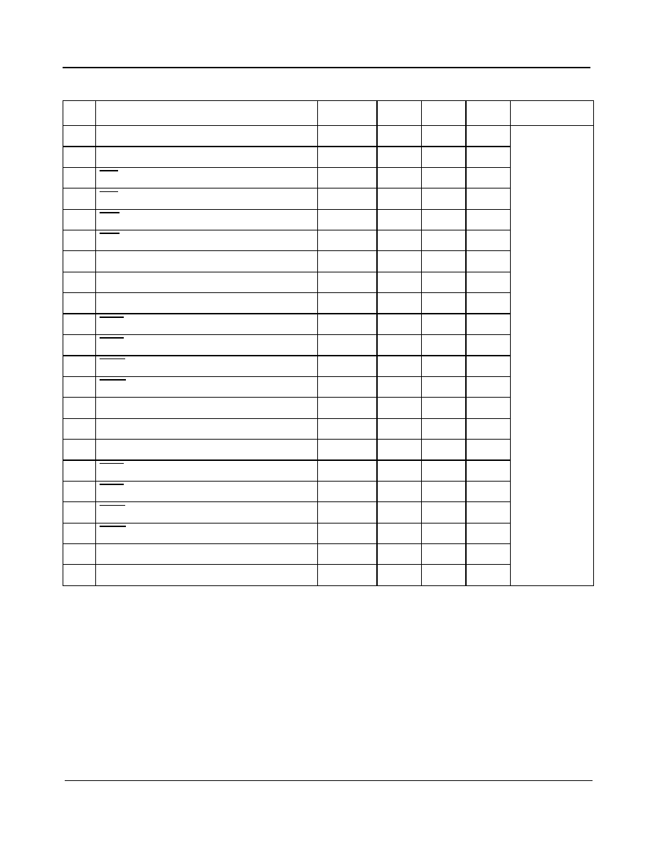
ZL30102
Data Sheet
42
Zarlink Semiconductor Inc.
* Supply voltage and operating temperature are as per Recommended Operating Conditions.
AC Electrical Characteristics* - E1 output timing (see Figure 27).
Characteristics
Sym.
Min.
Max.
Units
Notes
1
C2o delay
t
C2D
-0.4
0.3
ns
outputs loaded
with 30 pF
2
C2o pulse width low
t
C2L
243.0
244.1
ns
3
F4o pulse width low
t
F4L
243.3
244.3
ns
4
F4o delay
t
F4D
121.5
122.2
ns
5
C4o pulse width low
t
C4L
121.0
122.4
ns
6
C4o delay
t
C4D
-0.3
1.1
ns
7
F8o pulse width high
t
F8H
121.6
123.5
ns
8
C8o pulse width low
t
C8L
60.3
61.3
ns
9
C8o delay
t
C8D
-0.4
0.3
ns
10
F16o pulse with low
t
F16L
60.3
61.2
ns
11
F16o delay
t
F16D
29.9
30.8
ns
12
C16o pulse width low
t
C16L
28.7
30.8
ns
13
C16o delay
t
C16D
-0.5
1.5
ns
14
F32o pulse width high
t
F32H
30.0
32.1
ns
15
C32o pulse width low
t
C32L
14.7
15.5
ns
16
C32o delay
t
C32D
-0.5
0.5
ns
17
F65o pulse with low
t
F65L
14.7
15.5
ns
18
F65o delay
t
F65D
7.1
8.0
ns
19
C65o pulse width low
t
C65L
7.2
8.1
ns
20
C65o delay
t
C65D
-1.0
1.0
ns
21
Output clock and frame pulse rise time
t
OR
1.1
2.0
ns
22
Output clock and frame pulse fall time
t
OF
1.2
2.3
ns

ZL30102
Data Sheet
43
Zarlink Semiconductor Inc.
Figure 27 - E1 Output Timing Referenced to F8/F32o
t
F8H
t
F4D
F4o
C16o
F8o
t
F16L
F16o
C8o
C4o
C2o
t
F16D
t
F4L
t
C16D
t
C8D
t
C4D
t
C16L
t
C8L
t
C4L
t
C2L
t
F32H
C65o
F32o
t
F65L
F65o
C32o
t
F65D
t
C65D
t
C32D
t
C65L
t
C32L
F32o, C32o, F65o and C65o are drawn on a larger scale than the other waveforms in this diagram.
t
C2D

ZL30102
Data Sheet
44
Zarlink Semiconductor Inc.
* Supply voltage and operating temperature are as per Recommended Operating Conditions.
o
Figure 28 - DS1 Output Timing Referenced to F8/F32o
* Supply voltage and operating temperature are as per Recommended Operating Conditions.
Figure 29 - DS2 Output Timing Referenced to F8/F32o
AC Electrical Characteristics* - DS1 output timing (see Figure 28).
Characteristics
Sym.
Min.
Max.
Units
Notes
1
C1.5o delay
t
C1.5D
-0.6
0.6
ns
outputs loaded
with 30 pF
2
C1.5o pulse width low
t
C1.5L
323.1
324.0
ns
3
C3o delay
t
C3D
-0.7
0.5
ns
4
C3o pulse width low
t
C3L
161.1
162.0
ns
5
Output clock and frame pulse rise time
t
OR
1.1
2.0
ns
6
Output clock and frame pulse fall time
t
OF
1.2
2.3
ns
AC Electrical Characteristics* - DS2 output timing (see Figure 29).
Characteristics
Sym.
Min.
Max.
Units
Notes
1
C6o delay
t
C6D
-0.70
0.70
ns
outputs
loaded with
30 pF
2
C6o pulse width low
t
C6L
78.5
79.3
ns
3
Output clock and frame pulse rise time
t
OR
1.1
2.0
ns
4
Output clock and frame pulse fall time
t
OF
1.2
2.3
ns
F8_32o
t
C1.5D
t
C1.5L
C1.5o
t
C3D
t
C3L
C3o
F8_32o
t
C6D
C6o
t
C6L
ZL30102
Data Sheet
45
Zarlink Semiconductor Inc.
* Supply voltage and operating temperature are as per Recommended Operating Conditions.
AC Electrical Characteristics* - OSCi 20 MHz Master Clock Input
Characteristics
Min.
Max.
Units
Notes
1
Oscillator Tolerance - DS1
-32
+32
ppm
2
Oscillator Tolerance - E1
-50
+50
ppm
3
Duty cycle
40
60
%
4
Rise time
10
ns
5
Fall time
10
ns

ZL30102
Data Sheet
46
Zarlink Semiconductor Inc.
7.2 Performance Characteristics
* Supply voltage and operating temperature are as per Recommended Operating Conditions.
Performance Characteristics* - Functional
Characteristics
Min.
Max.
Units
Notes
1
Holdover accuracy
0.1
ppm
2
Holdover stability
0
ppm
Determined by stability of the
20 MHz master clock oscillator
3
Freerun accuracy
0
ppm
Determined by accuracy of the
20 MHz master clock oscillator
4
Capture range
-130
+130
ppm
The 20 MHz master clock oscillator
set at 0 ppm
Reference Out of Range Threshold
(including hysteresis)
5
DS1
-64
-83
+64
+83
ppm
The 20 MHz master clock oscillator
set at 0 ppm
6
E1
-100
-130
+100
+130
ppm
The 20 MHz master clock oscillator
set at 0 ppm
Lock Time
7
1.8 Hz filter
40
50
s
�64 ppm to �100 ppm frequency
offset, SEC_MSTR = 0, HMS = 1,
TIE_CLR = 1 and FASTLOCK=0
8
58 Hz filter (8 kHz reference)
15
15
s
�64 ppm to �100 ppm frequency
offset, SEC_MSTR = 1, HMS = 1,
TIE_CLR = 1 and FASTLOCK=0
9
922 Hz filter
1
1
s
�64 ppm to �100 ppm frequency
offset, SEC_MSTR = 1, HMS = 1,
TIE_CLR = 1 and FASTLOCK=0
10
fast lock
1
1
s
�64 ppm to �100 ppm frequency
offset and FASTLOCK=1
Output Phase Continuity (MTIE)
11
Reference switching
13
ns
TIE_CLR=1
12
Switching from Normal mode to
Holdover mode
0
ns
13
Switching from Holdover mode to
Normal mode
13
ns
TIE_CLR=1 and HMS=1
Output Phase Slope
14
primary master mode
61
�/s
SEC_MSTR=0
15
secondary master mode
9.5
ms/s
SEC_MSTR=1

ZL30102
Data Sheet
47
Zarlink Semiconductor Inc.
* Supply voltage and operating temperature are as per Recommended Operating Conditions.
* Supply voltage and operating temperature are as per Recommended Operating Conditions.
* Supply voltage and operating temperature are as per Recommended Operating Conditions.
* Supply voltage and operating temperature are as per Recommended Operating Conditions.
Performance Characteristics*: Input Wander and Jitter Tolerance Conformance
Input reference
frequency
Standard
Interface
1
1.544 MHz
Telcordia GR-1244-CORE
DS1 Line timing,
DS1 External timing
2
2.048 MHz
ITU-T G.823
2048 kbit/s
Performance Characteristics*: Output Jitter Generation - ANSI T1.403 conformance
Signal
ANSI T1.403
Jitter Generation Requirements
ZL30102
maximum jitter
generation
Units
Jitter
measurement
filter
Limit in
UI
Equivalent
limit in the
time domain
DS1 Interface
1
C1.5o (1.544 MHz)
8 kHz to 40 kHz
0.07 UI
pp
45.3
0.30
ns
pp
2
10 Hz to 40 kHz
0.5 UI
pp
324
0.32
ns
pp
Performance Characteristics*: Output Jitter Generation - ITU-T G.747 conformance
Signal
ITU-T G.747
Jitter Generation Requirements
ZL30102
maximum jitter
generation
Units
Jitter
measurement
filter
Limit in
UI
Equivalent
limit in the
time domain
DS2 Interface
1
C6o (6.312 MHz)
10 kHz to 60 kHz
0.05 UI
pp
7.92
0.20
ns
pp
Performance Characteristics*: Output Jitter Generation - ITU-T G.812 conformance
Signal
ITU-T
G.812
Jitter Generation Requirements
ZL30102
maximum jitter
generation
Units
Jitter
measurement
filter
Limit in
UI
Equivalent
limit in the
time domain
E1 Interface
1
C2o (2.048 MHz)
20 Hz to 100 kHz
0.05 UI
pp
24.4
0.36
ns
pp
ZL30102
Data Sheet
48
Zarlink Semiconductor Inc.
* Supply voltage and operating temperature are as per Recommended Operating Conditions.
Performance Characteristics* - Unfiltered Jitter Generation
Characteristics
Max.
[ns
pp
]
Notes
1
C1.5o (1.544 MHz)
0.45
2
C2o (2.048 MHz)
0.47
3
C3o (3.088 MHz)
0.53
4
C4o (4.096 MHz)
0.42
5
C6o (6.312 MHz)
0.58
6
C8o (8.192 MHz)
0.42
7
C16o (16.384 MHz)
0.56
8
C32o (32.768 MHz)
0.46
9
C65o (65.536 MHz)
0.49
10
F4o (8 kHz)
0.43
11
F8o (8 kHz)
0.43
12
F16o (8 kHz)
0.44
13
F32o (8 kHz)
0.43
14
F65o (8 kHz)
0.46

c Zarlink Semiconductor 2002 All rights reserved.
APPRD.
ISSUE
DATE
ACN
Package Code
Previous package codes

www.zarlink.com
Information relating to products and services furnished herein by Zarlink Semiconductor Inc. or its subsidiaries (collectively "Zarlink") is believed to be reliable.
However, Zarlink assumes no liability for errors that may appear in this publication, or for liability otherwise arising from the application or use of any such
information, product or service or for any infringement of patents or other intellectual property rights owned by third parties which may result from such application or
use. Neither the supply of such information or purchase of product or service conveys any license, either express or implied, under patents or other intellectual
property rights owned by Zarlink or licensed from third parties by Zarlink, whatsoever. Purchasers of products are also hereby notified that the use of product in
certain ways or in combination with Zarlink, or non-Zarlink furnished goods or services may infringe patents or other intellectual property rights owned by Zarlink.
This publication is issued to provide information only and (unless agreed by Zarlink in writing) may not be used, applied or reproduced for any purpose nor form part
of any order or contract nor to be regarded as a representation relating to the products or services concerned. The products, their specifications, services and other
information appearing in this publication are subject to change by Zarlink without notice. No warranty or guarantee express or implied is made regarding the
capability, performance or suitability of any product or service. Information concerning possible methods of use is provided as a guide only and does not constitute
any guarantee that such methods of use will be satisfactory in a specific piece of equipment. It is the user's responsibility to fully determine the performance and
suitability of any equipment using such information and to ensure that any publication or data used is up to date and has not been superseded. Manufacturing does
not necessarily include testing of all functions or parameters. These products are not suitable for use in any medical products whose failure to perform may result in
significant injury or death to the user. All products and materials are sold and services provided subject to Zarlink's conditions of sale which are available on request.
Purchase of Zarlink's I
2
C components conveys a licence under the Philips I
2
C Patent rights to use these components in and I
2
C System, provided that the system
conforms to the I
2
C Standard Specification as defined by Philips.
Zarlink, ZL and the Zarlink Semiconductor logo are trademarks of Zarlink Semiconductor Inc.
Copyright Zarlink Semiconductor Inc. All Rights Reserved.
TECHNICAL DOCUMENTATION - NOT FOR RESALE
For more information about all Zarlink products
visit our Web Site at