
1
Features
�
Broadband 1 to 2000MHz
�
Low Power (500mW)
�
3 Diff Outputs
�
6 Single Outputs
�
High Linearity
�
IIP3 = +20dBm
�
IIP2 = +50dBm
�
NF = 8dB
�
>40dB AGC Range
�
Ultra Fast AGC
�
Gain Tracking Error <1dB
Applications
�
RF Signal Switching
�
RF Signal Level Control
�
Phased Arrays
�
Instrumentation
�
ATE
�
Base Station RX and TX
�
Adaptive Antenna's Systems
�
Video Recorders
�
RF Signal Distribution
�
Multiple Tuners
�
Satellite, Cable, Terrestrial Digital TVMultiple
Tuners
Description
The ZL40000 is an ultra high linearity RF power divider.
The device provides a 75 Ohm Input impedance to a
broad band RF input Signal. The signal is buffered
through an ultra high linearity 6dB Gain buffer. This is
followed by a power divider which splits the buffered
signal into 3 signals. One signal is passed through a
200Ohm differential output driver. The other two signals
are passed through two separate 0 to �40dB AGC
stages before output as two isolated independent
differential Signals.
The device is built on Zarlink's 20GHz Complimentary
Bipolar Process.
April 2003
Ordering Information
ZL40000/LCE
28 MLP Tubes
ZL40000/LCF
28 MLP Tape & Reel
-40
o
C to +80
o
C
ZL40000
3/6 Channel DC to 2 GHz Power Splitter
Data Sheet
Figure 1 - Functional Block Diagram
RFin
RFinb
Out3
Out3b
Out2
Out2b
Out1
Out1b
AGC1
AGC2
BGR
Vcc
Vee
Vcc
Vee
Vee
Vee

ZL40000
Data Sheet
2
Figure 2 - Pin Diagram
Figure 3 - Application Diagram - A (Differential)
Vcc
N/C
Rfin
Rfinb
Vee
N/C
N/C
N/C
N/C
Vee
Vee
N/C
Out2
Out2b
N/C
N/C
Ou
t1
Ou
t1
b
Vee
AG
C
2
AG
C
1
Vcc
Vcc
Vcc
Ou
t3
Ou
t3
b
Vee
Vee
1
Vcc
N/C
Rfin
Rfinb
Vee
N/C
N/C
N/C
Vee
Vee
N/C
Out2
Out2b
Ve
e
Ou
t
1
Ou
t1
b
Ve
e
AGC
2
AGC
1
Vc
c
Vc
c
Ou
t
3
Ou
t
3
b
Ve
e
1
10nF
10nF
10nF
10nF
10nF
1:1
MABAES2009
50
/
7
5 O
h
m
1:1
MABAES2009
50/75 Ohm
2:1
50
/
7
5 O
h
m
10nF
Vcc
RFin

Data Sheet
ZL40000
3
Figure 4 - Application Diagram B (Single Ended)
Figure 5 - ZL40000 I/O Circuits
105 O
h
m
105 O
h
m
12mA
2.8V
1pF
1.0nH
1.0nH
12mA
Vagc
Out1& Out2
1pF
200 O
h
m
200 O
h
m
6mA
1.3V
0.5pF
1.0nH
1.0nH
Out3
0.5pF
2V
2K
30K
AGC1/
AGC2
75
1.0nH
1.0nH
2.5V
RFin
RFinb

ZL40000
Data Sheet
4
Absolute Maximum Ratings
Characteristic
Min
Max
Units
Comments
Supply Voltage (Vcc)
- 0.5
6
V
RFin
12
dBm
All I/O ports
-0.5V
Vcc+0.5
V
Storage Temperature
-55
150
�C
Junction Temperature
125
�C
ESD protection
2KV
Mil-std 883B / 3015 cat1
Operating Range
Characteristic
Min
Typ
Max
Units
Comments
Supply Voltage (Vcc)
4.75
5.25
V
AGC1
0
5.25
V
AGC2
0
5.25
V
RFin Frequency Range
0.1
2000
MHz
Operating Junction Temperature
-40
+120
�C
Junc'n to Amb't resistance Theta Ja
50
�C/W
4 layer FR4 Board
Junc'n to Case resistance Theta Jc
20
�C/W
4 layer FR4 Board
DC Electrical Characteristics -
Vcc=5V +/- 0.25V, Tamb = -40C to 80C, unless otherwise spec'd.
Characteristic
Min
Typ
Max
Units
Comments
Supply Current
100
130
m
Power Dissipation
500
683
mW
RFin, RFinb DC Level
Vcc/2
V
Out1, Out1b DC Level
Vcc-1.2
V
AGC1 = 0V
Out2, Out2b DC Level
Vcc-1.2
V
AGC2 = 0V
Out3, Out3b DC Level
Vcc-0.5
V

Data Sheet
ZL40000
5
AC Electrical Characteristics -
Vcc=5V +/- 0.25V, Tamb = -40C to 80C, unless otherwise spec'd.
Characteristic
Min
Typ
Max
Units
Comments
Diff RFin impedance
75
Ohm
S11
6
dB
(See Figure 36) (10MHz to 1000MHz)
Diff Out1 impedance
200
Ohm
Diff Out2 impedance
200
Ohm
Diff Out3 impedance
400
Ohm
S21 Gain1 (Out1/RFin)
3.5
6.5
9.5
dB
100 Ohm Diff load, AGC1=0V (Max Gain)
S21 Gain2 (Out2/RFin)
3.5
6.5
9.5
dB
100 Ohm Diff load, AGC1=0V (Max Gain)
S21 Gain3 (Out3/RFin)
-3.5
-0.5
-2.5
dB
200 Ohm Diff load,
Gain Matching (Gain1 - Gain2)
-0.5
0
0.5
dB
AGC1 = AGC2 = 0V (Max Gain)
Gain Matching (Gain1- Gain2)
-0.5
0.5
dB
Gain1 = Gain2 = 5dB to 0dB, Figure 16 & Figure
18.
Gain Matching (Gain1 - Gain2)
-2
2
dB
Gain1 = Gain2 = 0dB to �25dB,
Figure 17 & Figure 19 (Temp = 0C to 80C)
NF (Out1 & Out2)
7.5
dB
Figure 32 & Figure 33 (Gain = Max)
NF (Out1 & Out2)
12
dB
Figure 32 & Figure 33 (Gain = 0dB)
NF (Out1 & Out2)
15
dB
Figure 32 & Figure 33 (Gain = -5dB)
NF (Out1 & Out2)
18
dB
Figure 32 & Figure 33 (Gain = -10dB)
RFin P-dB compression
-2
0
dBm
CMRR
40
dB
AGC Range (Out1 & Out2)
40
dB
AGC �3dB BW
45
MHz
AGC Switching Time
15
ns
Max Gain to Min Gain (Vagc=0.8V to 4.2V)
AGC input referred Noise
200
nV/rt Hz
(Includes 26dB agc input resistor attenuator)
IIP3_100MHz
20
dBm
Figure 26 & Figure 27
IIP3_500MHz
17
dBm
Figure 26 & Figure 27
IIP3_1000MHz
13
dBm
Figure 26 & Figure 27
IIP3 variance / AGC
-1
1
dB
Gain = 5dB to � 10dB, Figure 28 & Figure 29
IIP2_50MHz
55
dBm
Figure 20 & Figure 21 (0dB Gain)
IIP2_500MHz
42
dBm
Figure 20 & Figure 21 (0dB Gain)
Isolation (Output to Output)
50
dB
Balanced to Balanced
Isolation (output to output)
25
Single Ch1 to Single Ch2 Output
S21 (Output to Input)
-40
dB
Balanced to Balanced

ZL40000
Data Sheet
6
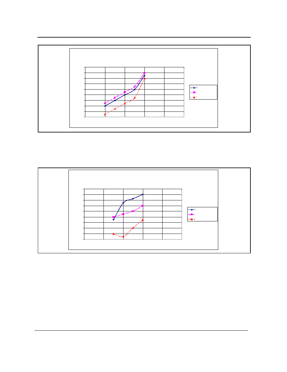
Figure 6 - Typical Ch1&2 Diff Gain / Freq / Vcc @ 25C
Figure 7 - Typical Ch3 Diff Gain / Freq / Vcc @ 25C
Out1 Diff Max Gain / Freq @ 25C / Vcc
4
4.5
5
5.5
6
6.5
60
260
460
660
860
1060
Frequency in MHz
Ga
in
in
d
B
4.75
5
5.5
Out3 Gain / Freq @25C / Vcc
(RL=200Ohms diff)
-1.0
-0.5
0.0
0.5
1.0
60
260
460
660
860
1060
RFin Freq MHZ
Ga
in
in
d
B
4.75
5
5.5

Data Sheet
ZL40000
7
Figure 8 - Typical Ch1 & Ch2 Diff Max Gain / Freq / Temp @ 5V Vcc
Figure 9 - Typical Ch3 Gain / Freq @ 5V / Temp (R1=200 Ohm)
Out1 Gain / Freq @ 5V /Temp
4
4.5
5
5.5
6
6.5
7
60
260
460
660
860
1060
RFin Freq in MHz
Ga
in
in
d
B
-40
25
80
Out3 Gain / Freq @ 5V Vcc / Temp (Rl=200Ohms diff)
-1.0
-0.5
0.0
0.5
1.0
60
260
460
660
860
1060
RFin Freq in MHz
Ga
in
in
d
B
-40
25
80

ZL40000
Data Sheet
8
Figure 10 - Typical Diff Max Gain / Frequency
Figure 11 - Typical Single Ended Max Gain / Frequency
Gain_diff_Max
0
1
2
3
4
5
6
7
8
0
500
1000
1500
2000
Frequency in MHz
Ga
in in dB
Gain_Single_Max
0
1
2
3
4
5
0
500
1000
1500
2000
Frequency in MHz
G
a
in in dB

Data Sheet
ZL40000
9
Figure 12 - Typical AGC / VCC @ 25C
Figure 13 - Typical AGC / Temp @ 5 V Vcc
AGC @ 25C / Vcc
(Rload = 100 ohms Diff)
-70.0
-60.0
-50.0
-40.0
-30.0
-20.0
-10.0
0.0
10.0
0
1
2
3
4
5
AGC Voltage
G
a
in
in
d
B
4.75
5
5.25
AGC @ 5V Vcc / Temp
(Rload = 100Ohms diff)
-70.0
-60.0
-50.0
-40.0
-30.0
-20.0
-10.0
0.0
10.0
0
1
2
3
4
5
AGC Voltage
G
a
in
in
d
B
-40
25
80

ZL40000
Data Sheet
10
Figure 14 - Typical AGC Range / Frequency (Differential Output with all channel loads balanced)
Figure 15 - Typical AGC Range / Frequency (Single Ended output)
Typ AGC Range (Min Gain / Max Gain ) / Frequency
(Differential output with all Channel loads balanced)
-90.0
-80.0
-70.0
-60.0
-50.0
-40.0
-30.0
10
100
1000
10000
Frequency in MHz
A
G
C
r
a
nge
i
n
dB
C
CH1diff_Ch2_bal
CH2diff_Ch1_bal
CH1sing_in_diff_out
CH2sing_in_diff_out
AGC Range (Gain_min/Gain_max)
(Single Side In or Out)
-90.0
-80.0
-70.0
-60.0
-50.0
-40.0
-30.0
10
100
1000
10000
Frequency in MHz
A
G
C
r
a
nge
i
n
dB
C
CH2a_diff_in
CH1a-single_in
Ch2a_single_in
CH2b_single_in

Data Sheet
ZL40000
11
Figure 16 - Typical Gain Matching / AGC @25C / Vcc
Figure 17 - Typical Gain Match 1 to 2 / Gain @ 25C / Vcc
Gain Match / Gain @25C / Vcc
(5dB to 0dB AGC range)
-0.3
-0.2
-0.1
0
0.1
0.2
0.3
5.23
5.21
5.14
5.01
4.69
4.14
3.38
2.39
1.29
0.02 -1.49
Typical Gain in dB
Gai
n
D
i
ffer
e
n
ce Ou
t2-Ou
t
1
Temp = 25C 4.75
Temp = 25C 4.75
Temp = 25C 5
Temp = 25C 5
Temp = 25C 5.25
Temp = 25C 5.25
Gain Match / Gain @ 25C / Vcc
( 0 to -30dB AGC Range)
-1
-0.8
-0.6
-0.4
-0.2
0
0.2
0.4
0.6
0.8
1
0.02
-1.49
-3.22
-5.54
-8.58
-12.73
-18.21
-24.54
-31.56
Typical Gain in dB
G
a
in D
i
ff O
u
t2
- O
u
t1
in dB
4.75
4.75
5
5
5.25
5.25

ZL40000
Data Sheet
12
Figure 18 - Typical Gain Matching / AGC @ 5V Vcc / Temp
Figure 19 - Typical Gain Matching / AGC @ 5V Vcc / Temp
Gain Match / Gain @ Vcc =5V / Temp
( 5dB to 0dB AGC Range)
-0.4
-0.3
-0.2
-0.1
0
0.1
0.2
0.3
0.4
5.23
5.21
5.14
5.01
4.69
4.14
3.38
2.39
1.29
0.02
-1.49
Typical Gain in dB
Gai
n
D
i
ffer
e
n
ce Ou
t2 -
O
u
t
1
in dB
-40
-40
25
25
80
80
Gain Matching / Gain @5V Vcc / Temp
(0 to - 30dB Gain Range)
-6
-4
-2
0
2
4
6
0.02
-1.49
-3.22
-5.54
-8.58
-12.73
-18.21
-24.54
-31.56
Typical Gain in dB
Gai
n
D
i
ff Ou
t2 -Ou
t
1 i
n
d
B
-40
-40
25
25
80
80

Data Sheet
ZL40000
13
Figure 20 - Typical Out1 @ Out2 IIP2 / Frequency @ Max Gain @ 25C / Vcc
Figure 21 - Typical Out1 @ Out2 IIP2 / Frequency @ Max Gain @ 5V Vcc / Temp
IIP2 Freq @ 25 C / Vcc
30
35
40
45
50
55
60
50
500
1000
Frequency in MHz
IIP
2
in dBM
4.75
4.75
5
5
5.25
5.25
IIP2 / Freq @ 5V Vcc / Temp @ Max Gain
30
35
40
45
50
55
60
65
50
500
1000
Freq in MHz
IIP2 in dBm
-40
-40
25
25
80
80

ZL40000
Data Sheet
14
Figure 22 - Typical IIP2 / Gain @ 25C / Vcc @ 500MHz
Figure 23 - Typical IIP2 / Gain @ 5V Vcc / Temp @ 500MHz
IIP2 / Gain @ 25C / Vcc
30
32
34
36
38
40
42
44
46
48
4
-1
-6
-11
Gain in dB
IIP
2
in dBm
4.75
5
5.25
IIP2 / Gain @ 5V Vcc / Temp
30
35
40
45
50
55
4
-1
-6
-11
Gain in dB
IIP
2
in
d
B
m
-40
25
80

Data Sheet
ZL40000
15
Figure 24 - Typical Differential IIP2 / Frequency / AGC Setting
Figure 25 - Typical Single Ended IIP2 / Frequency / AGC
Diff IIP2 / Frequency / AGC
0
10
20
30
40
50
60
0
500
1000
1500
2000
Frequency in MHz
IIP
2
in
d
B
m
IIP2_+6dB
IIP2_0dB
IIP2_-5dB
IIP2_-10dB
IIP2_-20dB
+6dB
0dB
-5dB
-10dB
-20dB
Single ended IIP2 / Frequency / AGC
-10
0
10
20
30
40
50
60
0
500
1000
1500
2000
Frequency in MHz
IIP
2
i
n
d
B
m
IIP2_3dB
IIP2_-5dB
IIP2_-10dB
IIP2_-20dB
+3dB
-5dB
-10dB
-20dB

ZL40000
Data Sheet
16
Figure 26 - Typical Out1, Out2 & Out3 IIP3 / Frequency @ Gain = Max / Vcc @ 25C
Figure 27 - Typical Out1, Out2 & Out3 IIP3 / Frequency @ Gain = Max / Temp @ 5V Vcc
IIP3 / Frequency @ Gain = Max / Vcc @ 25C
0
5
10
15
20
25
50
500
1000
Frequency in MHz
IIP
3
in
d
B
m
4.75
5
5.25
IIP3 / Freq @ Gain = Max / Temp @ Vcc=5V
0
5
10
15
20
25
50
500
1000
Frequency in MHz
IIP
3
in
d
B
m
-40
25
80

Data Sheet
ZL40000
17
Figure 28 - Typical IIP3 Variance with AGC @ Vcc=5V /Temp @ 400MHz
Figure 29 - Typical IIP3 variance with AGC @ 25C / Vcc @ 400MHz
IIP3 Variance / Gain @ Vcc=5V / Temp
-1.2
-1
-0.8
-0.6
-0.4
-0.2
0
0.2
0.4
0.6
0.8
4
-1
-6
-11
Gain in dB
De
lt
a
ga
in in dB
-40
25
80
IIP3 variance / AGC @25C / Vcc
-2
-1.5
-1
-0.5
0
0.5
1
4
-1
-6
-11
Gain in dB
De
lt
a
IIP
3
in dB
4.75
5
5.25

ZL40000
Data Sheet
18
Figure 30 - Typical IIP3 @ Max Gain Differential / Frequency
Figure 31 - Typical IIP3 Single Ended / Frequency / AGC
IIP3 / Frequency / AGC Setting
-10.0
-5.0
0.0
5.0
10.0
15.0
20.0
25.0
0
500
1000
1500
2000
Frequency in MHz
IIP
3
in
d
B
m
IIP3_+6dB
IIP3_0dB
IIP3_-5dB
IIP3_-10dB
IIP3_-20dB
-20dB
-5dB
6dB
0dB
-10dB
Single IIP3 / Frequency / AGC
-10.0
-5.0
0.0
5.0
10.0
15.0
20.0
25.0
0
500
1000
1500
2000
Frequency in MHz
S
i
ngl
e E
nded I
I
P
3 i
n
dB
m
IIP3_3dB
IIP3_-5dB
IIP3_-10dB
IIP3_-20dB
+3dB
-5dB
-10dB
-20dB

Data Sheet
ZL40000
19
Figure 32 - Typical Differential NF / Frequency @ 25C / Vcc @ Max Gain
Figure 33 - Typical Differential NF / Frequency @ 5V Vcc / Temp @ Max Gain
Out1 & Out2 NF / Frequency @ 25C / Vcc @ Max gain
6.0
6.5
7.0
7.5
8.0
8.5
9.0
50
300
600
1000
Frequency in MHz
N
F
in
d
B
4.75
5
5.25
NF / Frequency @ 5V Vcc / Temp @ Max Gain
6.0
6.5
7.0
7.5
8.0
8.5
9.0
50
300
600
1000
Frequency in MHz
N
F
in dB
-40
25
80

ZL40000
Data Sheet
20
Figure 34 - Typical Differential NF / Gain @ 5V Vcc / Temp measured @ 600MHz
Figure 35 - Typical Differential NF / Gain @ 25C / Vcc measured @ 600MHz
0.0
2.0
4.0
6.0
8.0
10.0
12.0
14.0
16.0
18.0
20.0
5
0
-5
-10
Gain in dB
NF in dB
4.75
5
5.25
NF / Gain @ 5V Vcc / Temp measured @ 600MHz
NF / Gain @ 5V Vcc / Temp @ 600MHz
0
2
4
6
8
10
12
14
16
18
20
5
0
-5
-10
Gain in dB
N
F
in
d
B
-40
25
80

Data Sheet
ZL40000
21
Figure 36 - Typical S11 in 50Ohm System
Figure 37 - Typical Differential CSO / Level per Channel @ Max Gain
CH136, CH117 and CH76 @ 850MHz, 745MHZ and 499MHz respectively) (Composite signal contains 130
Channels at 6MHz spacing between 50MHz and 850 MHz)
S11 / Frequency @ 25C / Vcc
-12
-10
-8
-6
-4
-2
0
50
300
600
1000
Frequency in MHz
S
11 i
n
dB
4.75
5
5.25
ZL40000 Typ Diff CSO1 @ Max Gain / dBmV per Ch / Ch number
-80
-75
-70
-65
-60
-55
-50
10.0
12.0
14.0
16.0
18.0
20.0
Power per Ch in dBmV / Ch
C
S
O
@
1.
25M
H
z
i
n
d
B
C
Ch135_CSO1
Ch117_CSO1
Ch76_CSO1
ZL40000
Data Sheet
22
Figure 38 - Typical Differential CTB / Level per Channel @ Max Gain
CH136, CH117 and CH76 @ 850MHz, 745MHZ and 499MHz respectively) (Composite signal contains 130
Channels at 6MHz spacing between 50MHz and 850 MHz)
Figure 39 - Typical Differential CSO / Level per Channel @ -12dB Gain
(CH136, CH117 and CH76 @ 850MHz, 745MHZ and 499MHz respectively) (Composite signal contains 130
Channels at 6MHz spacing between 50MHz and 850 MHz)
ZL40000 Typ Diff CTB / Power per Ch / Ch number
-68
-66
-64
-62
-60
-58
-56
-54
-52
-50
10.0
12.0
14.0
16.0
18.0
20.0
Power per Ch in dBmV
CT
B in
d
B
C
Ch135_CTB
Ch117_CTB
Ch76_CTB
ZL40000 Typ Diff CSO1 @ -18dB AGC / Ch power / Ch number
-68
-66
-64
-62
-60
-58
-56
-54
-52
-50
10.0
12.0
14.0
16.0
18.0
20.0
Ch power in dBmV
CS
O
1
@
-
12d
BAG
C in
d
B
C
Ch135_CSO1
Ch117_CSO1
Ch76_CSO1

Data Sheet
ZL40000
23
Figure 40 - CH136, CH117 and CH76 @ 850MHz, 745MHZ and 499MHz respectively
(Composite signal contains 130 Channels at 6MHz spacing between 50MHz and 850 MHz)
ZL40000 Typ Diff CTB @ -18dB AGC / Ch power / Ch number
-70
-68
-66
-64
-62
-60
-58
-56
-54
-52
-50
10.0
12.0
14.0
16.0
18.0
20.0
Ch power in dBmV
CT
B in
d
B
C
Ch135_CTB
Ch117_CTB
Ch76_CTB

ZL40000
Data Sheet
24
Applications Notes
The ZL40000 is a wide band RF signal conditioning and distribution circuit that can be used in many applications.
The device has excellent signal handling performance and provides > 40 dB of AGC range over the full operating
BW of DC to 2GHz.
The device excellent dynamic performance and wide bandwidth make the device ideally suited to providing a
separate buffered RF multi carrier signal to multiple tuner applications such as can be found in next generation Set
Top Boxes, VCRs, DVDs and TVs for Digital Terrestrial, Cable and Satellite.
The device will also satisfy Analogue Terrestrial, Cable and Satellite requirements up to -35dBm / Ch in 130 Carrier
Composite signals from 50MHz to 850 MHz with 6MHz channel spacing.
The very high signal handling RF AGC stage makes the ZL40000 suitable for use in all wide dynamic range receiver
systems operating in the 1MHz to 2GHz band.
The ZL40000 has excellent RF AGC performance providing > 40dB AGC range over the full DC to 2GHz operating
range. The RF AGC range exceeds 60dBC from DC to 500MHz.
Both the excellent RF AGC range and the excellent Multi Carrier performance are achieved as a result of the
balanced nature of the circuit. The ZL40000 can be operated both single ended or differential at both the input and
the output.
The performance achieved with the output signal used differential, increases the RF isolation and adds 20dB
improvement above that achieved single ended. It also greatly reduces the second order distortion and inter
modulation present at the output.
The best performance is achieved when all output ports are connected to balanced loads and if a particular channel
is to be used single ended output, the unused output should be terminated with a matching load.
The excellent RF range and high BW AGC control port makes the ZL40000 suitable for applications in which fast
level control or RF Signal Switching is required such as may be found in Instrumentation.
The RF AGC attenuator can be switched through 60dB of AGC range typically 15nS.
A pair of ZL4000 with cross coupled outputs and a broad band quadrature phase shift unit can be used to build a
broad band RF phase rotator that could be used in Agile Active Antenna Arrays for Transmitters with fast beam
steering.


www.zarlink.com
Information relating to products and services furnished herein by Zarlink Semiconductor Inc. trading as Zarlink Semiconductor or its subsidiaries (collectively
"Zarlink") is believed to be reliable. However, Zarlink assumes no liability for errors that may appear in this publication, or for liability otherwise arising from the
application or use of any such information, product or service or for any infringement of patents or other intellectual property rights owned by third parties which may
result from such application or use. Neither the supply of such information or purchase of product or service conveys any license, either express or implied, under
patents or other intellectual property rights owned by Zarlink or licensed from third parties by Zarlink, whatsoever. Purchasers of products are also hereby notified
that the use of product in certain ways or in combination with Zarlink, or non-Zarlink furnished goods or services may infringe patents or other intellectual property
rights owned by Zarlink.
This publication is issued to provide information only and (unless agreed by Zarlink in writing) may not be used, applied or reproduced for any purpose nor form part
of any order or contract nor to be regarded as a representation relating to the products or services concerned. The products, their specifications, services and other
information appearing in this publication are subject to change by Zarlink without notice. No warranty or guarantee express or implied is made regarding the
capability, performance or suitability of any product or service. Information concerning possible methods of use is provided as a guide only and does not constitute
any guarantee that such methods of use will be satisfactory in a specific piece of equipment. It is the user's responsibility to fully determine the performance and
suitability of any equipment using such information and to ensure that any publication or data used is up to date and has not been superseded. Manufacturing does
not necessarily include testing of all functions or parameters. These products are not suitable for use in any medical products whose failure to perform may result in
significant injury or death to the user. All products and materials are sold and services provided subject to Zarlink's conditions of sale which are available on request.
Purchase of Zarlink's I
2
C components conveys a licence under the Philips I
2
C Patent rights to use these components in an I
2
C System, provided that the system
conforms to the I
2
C Standard Specification as defined by Philips.
Zarlink, ZL and the Zarlink Semiconductor logo are trademarks of Zarlink Semiconductor Inc.
Copyright 2003, Zarlink Semiconductor Inc. All Rights Reserved.
TECHNICAL DOCUMENTATION - NOT FOR RESALE
For more information about all Zarlink products
visit our Web Site at