1
Zarlink Semiconductor Inc.
Zarlink, ZL and the Zarlink Semiconductor logo are trademarks of Zarlink Semiconductor Inc.
Copyright 2003, Zarlink Semiconductor Inc. All Rights Reserved.
Applications
� Ethernet Pseudo-Wires across a Packet Switch
Network
Features
Ethernet Pseudo-Wire Emulation Functions
Supports the following functions for Ethernet Pseudo-
Wire emulation over the packet domain:
� Transports the complete Ethernet frame (less
preamble and FCS) across the PSN
� Supports up to 128 point-to-point pseudo-wire
links across the PSN
� VLAN priority field may be used to determine
class of service on the PSN
� complies with the standards for Ethernet pseudo-
wires proposed in the IETF's PWE3 working
group
Network Interfaces
� 3 x 100Mbit/s MII interfaces
� Handles maximum size Ethernet frames (up to
1522 bytes)
System Interfaces
� Flexible 32 bit host CPU interface (Motorola
PowerQUICCTM
II
compatible)
� Dual address DMA transfer of packets to or from
the CPU
� On-chip packet memory for self-contained
operation
Packet Processing Functions
� Flexible, multi-protocol packet encapsulation, with
support for IPv4/6, MPLS, L2TP, PWE3
� Wire speed processing and forwarding of packets
� Packet sequencing and re-ordering where
required
� Four classes of service with programmable
priority mechanisms (WFQ and SP)
� Flexible classification of incoming packets at
layers 2, 3, 4 and 5
November 2003
Ordering Information
ZL50130 PBGA
-40
�
C to +85
�
C
ZL50130
Ethernet Pseudo-Wires across a PSN
Data Sheet
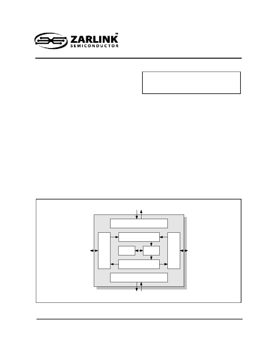
Figure 1 - High Level Overview
packet
receive/classifier
packet transmit
- add layer 2/3 headers
task
manager
memory management /
on-chip packet memory
Host Processor Interface
with DMA support
protocol
engine
MAC
MAC
Optional Off-chip Packet Memory
0-8 MBytes SSRAM
Host Processor Interface
Motorola PowerQUICC
TM
II compatible
P
ack
et S
w
it
c
h
e
d
N
e
tw
ork
Int
e
rface
10
0 Mb
it/s
M
I
I
Cu
s
t
omer
E
n
d
S
e
rv
ices
10
0 Mb
it/s
M
I
I
ZL50130
Data Sheet
2
Zarlink Semiconductor Inc.
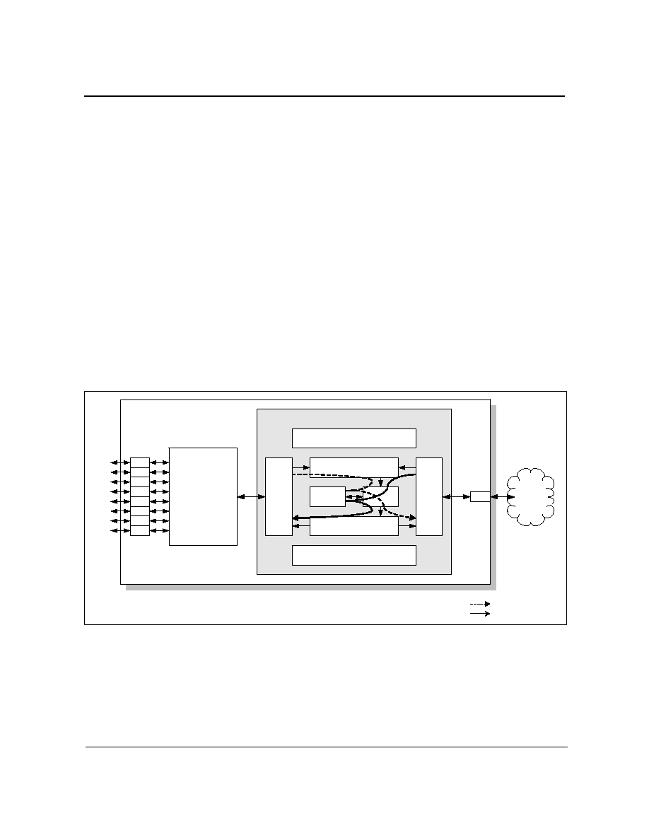
Description
The ZL50130 is part of a range of highly functional bridging devices. It provides the capability to extend a Local
Area Network based on Ethernet across a service provider's packet switched network. This allows a company with
multiple sites to manage its network as though it was a single LAN.
In conjunction with an Ethernet aggregation network, the ZL50130 provides the dataplane requirements of the inter-
working function between the customer end services and the provider's packet switched network (see Figure 2). It
can support wire-speed processing of up to 100 Mbit/s of traffic in each direction, and provides up to 128 separate
pseudo-wire connections across the PSN. Packets arriving from a single customer end service may all be directed
onto a single pseudo-wire, or split across multiple connections based on source and destination addresses. This is
useful in the case where the customer is using the Ethernet pseudo-wire service to connect multiple sites.
On packet egress the device includes four different classes of service, allowing priority treatment of customer traffic,
depending on the service level agreement between the customer and provider. The user priority field in the packet's
VLAN tag (if any) may be used to determine the appropriate class of service to be used on the PSN.
Packets received from the Ethernet interfaces are parsed to determine the egress destination, and are
appropriately queued to the customer end service, passed up to the host processor, or sent back toward the packet
interface. Again there are four different classes of service to allow differentiation between customers with different
service level agreements, or based on the use of VLAN tag priority.
The ZL50130 includes sufficient on-chip memory to allow completely self-contained operation, reducing system
costs and simplifying the design. For applications that do require more memory (e.g. where the network has a very
high packet delay variation), the device supports up to 8 Mbytes of external synchronous ZBT SRAM.
Figure 2 - Provider Edge Inter-working Function using the ZL50130
Provider Edge
Interworking Function
Ethernet
Switch
e.g. MVTX2604
MVTX2804
aggregation and
adaptation
functions
Phy
Phy
Phy
Phy
Phy
Phy
Phy
Phy
Phy
C
u
st
omer
End Serv
ic
es
PSN bound flow
CE bound flow
ZL50130 Ethernet Pseudo-Wire Device
packet
receive/classifier
packet transmit
- add layer 2/3 headers
task
manager
memory management /
on-chip packet memory
Host Processor Interface
with DMA support
protocol
engine
MAC
MAC
Packet
Switch
Network

ZL50130
Data Sheet
Table of Contents
3
Zarlink Semiconductor Inc.
Applications . . . . . . . . . . . . . . . . . . . . . . . . . . . . . . . . . . . . . . . . . . . . . . . . . . . . . . . . . . . . . . . . . . . . . . . . . . . . . 1
Features . . . . . . . . . . . . . . . . . . . . . . . . . . . . . . . . . . . . . . . . . . . . . . . . . . . . . . . . . . . . . . . . . . . . . . . . . . . . . . . . . 1
Description . . . . . . . . . . . . . . . . . . . . . . . . . . . . . . . . . . . . . . . . . . . . . . . . . . . . . . . . . . . . . . . . . . . . . . . . . . . . . . 2
1.0 Introduction . . . . . . . . . . . . . . . . . . . . . . . . . . . . . . . . . . . . . . . . . . . . . . . . . . . . . . . . . . . . . . . . . . . . . . . . . . . 7
1.1 Overview . . . . . . . . . . . . . . . . . . . . . . . . . . . . . . . . . . . . . . . . . . . . . . . . . . . . . . . . . . . . . . . . . . . . . . . . . . . 7
1.2 Basic Operation . . . . . . . . . . . . . . . . . . . . . . . . . . . . . . . . . . . . . . . . . . . . . . . . . . . . . . . . . . . . . . . . . . . . . . 7
1.2.1 PSN-Bound Flow . . . . . . . . . . . . . . . . . . . . . . . . . . . . . . . . . . . . . . . . . . . . . . . . . . . . . . . . . . . . . . . . 8
1.2.2 CE-Bound Flow . . . . . . . . . . . . . . . . . . . . . . . . . . . . . . . . . . . . . . . . . . . . . . . . . . . . . . . . . . . . . . . . . 8
1.2.3 Host Packet Generation. . . . . . . . . . . . . . . . . . . . . . . . . . . . . . . . . . . . . . . . . . . . . . . . . . . . . . . . . . . 8
1.2.4 External Memory Requirement . . . . . . . . . . . . . . . . . . . . . . . . . . . . . . . . . . . . . . . . . . . . . . . . . . . . . 8
2.0 Functional Block Descriptions . . . . . . . . . . . . . . . . . . . . . . . . . . . . . . . . . . . . . . . . . . . . . . . . . . . . . . . . . . . . 9
2.1 Task Manager . . . . . . . . . . . . . . . . . . . . . . . . . . . . . . . . . . . . . . . . . . . . . . . . . . . . . . . . . . . . . . . . . . . . . . . 9
2.2 Protocol Engine . . . . . . . . . . . . . . . . . . . . . . . . . . . . . . . . . . . . . . . . . . . . . . . . . . . . . . . . . . . . . . . . . . . . . . 9
2.3 Packet Transmit. . . . . . . . . . . . . . . . . . . . . . . . . . . . . . . . . . . . . . . . . . . . . . . . . . . . . . . . . . . . . . . . . . . . . 10
2.4 Packet Receive . . . . . . . . . . . . . . . . . . . . . . . . . . . . . . . . . . . . . . . . . . . . . . . . . . . . . . . . . . . . . . . . . . . . . 10
2.4.1 Packet Classification . . . . . . . . . . . . . . . . . . . . . . . . . . . . . . . . . . . . . . . . . . . . . . . . . . . . . . . . . . . . 11
2.4.2 Classifier Operation . . . . . . . . . . . . . . . . . . . . . . . . . . . . . . . . . . . . . . . . . . . . . . . . . . . . . . . . . . . . . 11
2.5 Ethernet MAC . . . . . . . . . . . . . . . . . . . . . . . . . . . . . . . . . . . . . . . . . . . . . . . . . . . . . . . . . . . . . . . . . . . . . . 12
2.6 Memory Management Unit . . . . . . . . . . . . . . . . . . . . . . . . . . . . . . . . . . . . . . . . . . . . . . . . . . . . . . . . . . . . 13
2.7 Host Interface . . . . . . . . . . . . . . . . . . . . . . . . . . . . . . . . . . . . . . . . . . . . . . . . . . . . . . . . . . . . . . . . . . . . . . 13
2.8 JTAG Interface and Board Level Test Features. . . . . . . . . . . . . . . . . . . . . . . . . . . . . . . . . . . . . . . . . . . . . 14
3.0 External Interface Description . . . . . . . . . . . . . . . . . . . . . . . . . . . . . . . . . . . . . . . . . . . . . . . . . . . . . . . . . . . 14
3.1 Packet Interfaces. . . . . . . . . . . . . . . . . . . . . . . . . . . . . . . . . . . . . . . . . . . . . . . . . . . . . . . . . . . . . . . . . . . . 14
3.2 External Memory Interface . . . . . . . . . . . . . . . . . . . . . . . . . . . . . . . . . . . . . . . . . . . . . . . . . . . . . . . . . . . . 23
3.3 CPU Interface . . . . . . . . . . . . . . . . . . . . . . . . . . . . . . . . . . . . . . . . . . . . . . . . . . . . . . . . . . . . . . . . . . . . . . 25
3.4 System Function Interface. . . . . . . . . . . . . . . . . . . . . . . . . . . . . . . . . . . . . . . . . . . . . . . . . . . . . . . . . . . . . 28
3.5 Test Facilities. . . . . . . . . . . . . . . . . . . . . . . . . . . . . . . . . . . . . . . . . . . . . . . . . . . . . . . . . . . . . . . . . . . . . . . 28
3.5.1 Administration and Control Interface . . . . . . . . . . . . . . . . . . . . . . . . . . . . . . . . . . . . . . . . . . . . . . . . 28
3.5.2 JTAG Interface . . . . . . . . . . . . . . . . . . . . . . . . . . . . . . . . . . . . . . . . . . . . . . . . . . . . . . . . . . . . . . . . . 29
3.6 Miscellaneous Inputs . . . . . . . . . . . . . . . . . . . . . . . . . . . . . . . . . . . . . . . . . . . . . . . . . . . . . . . . . . . . . . . . . 29
3.7 Power and Ground Connections . . . . . . . . . . . . . . . . . . . . . . . . . . . . . . . . . . . . . . . . . . . . . . . . . . . . . . . . 30
4.0 Miscellaneous . . . . . . . . . . . . . . . . . . . . . . . . . . . . . . . . . . . . . . . . . . . . . . . . . . . . . . . . . . . . . . . . . . . . . . . . 30
4.1 JTAG Interface and Board Level Test Features. . . . . . . . . . . . . . . . . . . . . . . . . . . . . . . . . . . . . . . . . . . . . 30
4.2 External Component Requirements . . . . . . . . . . . . . . . . . . . . . . . . . . . . . . . . . . . . . . . . . . . . . . . . . . . . . 30
4.3 Miscellaneous Features. . . . . . . . . . . . . . . . . . . . . . . . . . . . . . . . . . . . . . . . . . . . . . . . . . . . . . . . . . . . . . . 31
5.0 Memory Map and Register definitions . . . . . . . . . . . . . . . . . . . . . . . . . . . . . . . . . . . . . . . . . . . . . . . . . . . . . 31
6.0 Test Modes Operation . . . . . . . . . . . . . . . . . . . . . . . . . . . . . . . . . . . . . . . . . . . . . . . . . . . . . . . . . . . . . . . . . . 31
6.1 Overview . . . . . . . . . . . . . . . . . . . . . . . . . . . . . . . . . . . . . . . . . . . . . . . . . . . . . . . . . . . . . . . . . . . . . . . . . . 31
6.1.1 System Normal Mode. . . . . . . . . . . . . . . . . . . . . . . . . . . . . . . . . . . . . . . . . . . . . . . . . . . . . . . . . . . . 31
6.1.2 System Tri-State Mode . . . . . . . . . . . . . . . . . . . . . . . . . . . . . . . . . . . . . . . . . . . . . . . . . . . . . . . . . . 31
6.2 Test Mode Control . . . . . . . . . . . . . . . . . . . . . . . . . . . . . . . . . . . . . . . . . . . . . . . . . . . . . . . . . . . . . . . . . . . 31
6.3 System Normal Mode . . . . . . . . . . . . . . . . . . . . . . . . . . . . . . . . . . . . . . . . . . . . . . . . . . . . . . . . . . . . . . . . 31
6.4 System Tri-state Mode . . . . . . . . . . . . . . . . . . . . . . . . . . . . . . . . . . . . . . . . . . . . . . . . . . . . . . . . . . . . . . . 31
7.0 DC Characteristics. . . . . . . . . . . . . . . . . . . . . . . . . . . . . . . . . . . . . . . . . . . . . . . . . . . . . . . . . . . . . . . . . . . . . 32
7.1 Absolute Maximum Ratings. . . . . . . . . . . . . . . . . . . . . . . . . . . . . . . . . . . . . . . . . . . . . . . . . . . . . . . . . . . . 32
7.2 Recommended Operating Conditions . . . . . . . . . . . . . . . . . . . . . . . . . . . . . . . . . . . . . . . . . . . . . . . . . . . . 32
7.3 DC Characteristics. . . . . . . . . . . . . . . . . . . . . . . . . . . . . . . . . . . . . . . . . . . . . . . . . . . . . . . . . . . . . . . . . . . 33
7.4 Input Levels . . . . . . . . . . . . . . . . . . . . . . . . . . . . . . . . . . . . . . . . . . . . . . . . . . . . . . . . . . . . . . . . . . . . . . . . 33
7.5 Output Levels . . . . . . . . . . . . . . . . . . . . . . . . . . . . . . . . . . . . . . . . . . . . . . . . . . . . . . . . . . . . . . . . . . . . . . 33
8.0 AC Characteristics. . . . . . . . . . . . . . . . . . . . . . . . . . . . . . . . . . . . . . . . . . . . . . . . . . . . . . . . . . . . . . . . . . . . . 34
8.1 Packet Interface Timing. . . . . . . . . . . . . . . . . . . . . . . . . . . . . . . . . . . . . . . . . . . . . . . . . . . . . . . . . . . . . . . 34

ZL50130
Data Sheet
Table of Contents
4
Zarlink Semiconductor Inc.
8.1.1 MII Transmit Timing . . . . . . . . . . . . . . . . . . . . . . . . . . . . . . . . . . . . . . . . . . . . . . . . . . . . . . . . . . . . . 34
8.1.2 MII Receive Timing . . . . . . . . . . . . . . . . . . . . . . . . . . . . . . . . . . . . . . . . . . . . . . . . . . . . . . . . . . . . . 35
8.1.3 Management Interface Timing . . . . . . . . . . . . . . . . . . . . . . . . . . . . . . . . . . . . . . . . . . . . . . . . . . . . . 36
8.2 External Memory Interface Timing. . . . . . . . . . . . . . . . . . . . . . . . . . . . . . . . . . . . . . . . . . . . . . . . . . . . . . . 37
8.3 CPU Interface Timing . . . . . . . . . . . . . . . . . . . . . . . . . . . . . . . . . . . . . . . . . . . . . . . . . . . . . . . . . . . . . . . . 38
8.4 System Function Port . . . . . . . . . . . . . . . . . . . . . . . . . . . . . . . . . . . . . . . . . . . . . . . . . . . . . . . . . . . . . . . . 41
8.5 JTAG Interface Timing. . . . . . . . . . . . . . . . . . . . . . . . . . . . . . . . . . . . . . . . . . . . . . . . . . . . . . . . . . . . . . . . 42
9.0 Power Up sequence. . . . . . . . . . . . . . . . . . . . . . . . . . . . . . . . . . . . . . . . . . . . . . . . . . . . . . . . . . . . . . . . . . . . 44
10.0 Design and Layout Guidelines . . . . . . . . . . . . . . . . . . . . . . . . . . . . . . . . . . . . . . . . . . . . . . . . . . . . . . . . . . 45
10.1 High Speed Clock & Data Interfaces . . . . . . . . . . . . . . . . . . . . . . . . . . . . . . . . . . . . . . . . . . . . . . . . . . . . 45
10.1.1 External Memory Interface - special considerations during layout. . . . . . . . . . . . . . . . . . . . . . . . . 45
10.1.2 MAC Interface - special considerations during layout . . . . . . . . . . . . . . . . . . . . . . . . . . . . . . . . . . 46
10.1.3 Summary . . . . . . . . . . . . . . . . . . . . . . . . . . . . . . . . . . . . . . . . . . . . . . . . . . . . . . . . . . . . . . . . . . . . 46
10.2 CPU TA Output . . . . . . . . . . . . . . . . . . . . . . . . . . . . . . . . . . . . . . . . . . . . . . . . . . . . . . . . . . . . . . . . . . . . 46
11.0 Physical Specification . . . . . . . . . . . . . . . . . . . . . . . . . . . . . . . . . . . . . . . . . . . . . . . . . . . . . . . . . . . . . . . . . 47
12.0 Reference Documents . . . . . . . . . . . . . . . . . . . . . . . . . . . . . . . . . . . . . . . . . . . . . . . . . . . . . . . . . . . . . . . . . 55
12.1 External Standards/Specifications. . . . . . . . . . . . . . . . . . . . . . . . . . . . . . . . . . . . . . . . . . . . . . . . . . . . . . 55
12.2 Zarlink ZL50130 Product Related Documentation. . . . . . . . . . . . . . . . . . . . . . . . . . . . . . . . . . . . . . . . . . 55
13.0 Related Products . . . . . . . . . . . . . . . . . . . . . . . . . . . . . . . . . . . . . . . . . . . . . . . . . . . . . . . . . . . . . . . . . . . . . 55
14.0 Glossary . . . . . . . . . . . . . . . . . . . . . . . . . . . . . . . . . . . . . . . . . . . . . . . . . . . . . . . . . . . . . . . . . . . . . . . . . . . . 55

ZL50130
Data Sheet
List of Figures
5
Zarlink Semiconductor Inc.
Figure 1 - High Level Overview . . . . . . . . . . . . . . . . . . . . . . . . . . . . . . . . . . . . . . . . . . . . . . . . . . . . . . . . . . . . . . . . 1
Figure 2 - Provider Edge Inter-working Function using the ZL50130. . . . . . . . . . . . . . . . . . . . . . . . . . . . . . . . . . . . 2
Figure 3 - ZL50130 Operation . . . . . . . . . . . . . . . . . . . . . . . . . . . . . . . . . . . . . . . . . . . . . . . . . . . . . . . . . . . . . . . . . 7
Figure 4 - ZL50130 Data Flows . . . . . . . . . . . . . . . . . . . . . . . . . . . . . . . . . . . . . . . . . . . . . . . . . . . . . . . . . . . . . . . . 7
Figure 5 - Task Manager Routing Concept . . . . . . . . . . . . . . . . . . . . . . . . . . . . . . . . . . . . . . . . . . . . . . . . . . . . . . . 9
Figure 6 - MII Transmit Timing Diagram. . . . . . . . . . . . . . . . . . . . . . . . . . . . . . . . . . . . . . . . . . . . . . . . . . . . . . . . . 34
Figure 7 - MII Receive Timing Diagram . . . . . . . . . . . . . . . . . . . . . . . . . . . . . . . . . . . . . . . . . . . . . . . . . . . . . . . . . 35
Figure 8 - Management Interface Timing for Ethernet Port - Read . . . . . . . . . . . . . . . . . . . . . . . . . . . . . . . . . . . . 36
Figure 9 - Management Interface Timing for Ethernet Port - Write . . . . . . . . . . . . . . . . . . . . . . . . . . . . . . . . . . . . 36
Figure 10 - External RAM Read and Write timing . . . . . . . . . . . . . . . . . . . . . . . . . . . . . . . . . . . . . . . . . . . . . . . . . 37
Figure 11 - CPU Read - MPC8260. . . . . . . . . . . . . . . . . . . . . . . . . . . . . . . . . . . . . . . . . . . . . . . . . . . . . . . . . . . . . 39
Figure 12 - CPU Write - MPC8260. . . . . . . . . . . . . . . . . . . . . . . . . . . . . . . . . . . . . . . . . . . . . . . . . . . . . . . . . . . . . 39
Figure 13 - CPU DMA Read - MPC8260 . . . . . . . . . . . . . . . . . . . . . . . . . . . . . . . . . . . . . . . . . . . . . . . . . . . . . . . . 40
Figure 14 - CPU DMA Write - MPC8260 . . . . . . . . . . . . . . . . . . . . . . . . . . . . . . . . . . . . . . . . . . . . . . . . . . . . . . . . 40
Figure 15 - JTAG Signal Timing . . . . . . . . . . . . . . . . . . . . . . . . . . . . . . . . . . . . . . . . . . . . . . . . . . . . . . . . . . . . . . . 43
Figure 16 - JTAG Clock and Reset Timing. . . . . . . . . . . . . . . . . . . . . . . . . . . . . . . . . . . . . . . . . . . . . . . . . . . . . . . 43
Figure 17 - Powering Up the ZL50130. . . . . . . . . . . . . . . . . . . . . . . . . . . . . . . . . . . . . . . . . . . . . . . . . . . . . . . . . . 44
Figure 18 - CPU_TA Board Circuit . . . . . . . . . . . . . . . . . . . . . . . . . . . . . . . . . . . . . . . . . . . . . . . . . . . . . . . . . . . . . 46
Figure 19 - ZL50130 Package View and Ball Positions . . . . . . . . . . . . . . . . . . . . . . . . . . . . . . . . . . . . . . . . . . . . . 48