ZL50211
Data Sheet
4
Zarlink Semiconductor Inc.
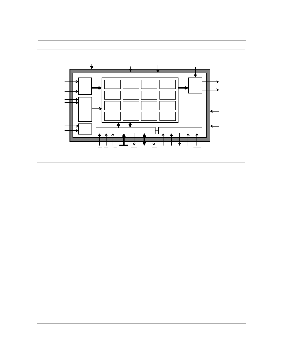
Pin Description
Signal
Name
Signal
Type
BGA Ball #
Signal
Description
V
DD1
= 3.3V
(V
DD_IO
)
Power
AC5,AC26,AC27,AD26,AD5,AE5,AF12,AF13,AF1
4,AF17,AF18,AF19,AF24,AF6,AF7,AF8,AG24,AH
24,E13,E14,E17,E18,E19,E23,E24,E25,E6,E7,E8,
F5,G26,G27,G5,H26,H5,M26,M5,N26,N5,P26,P27
, P4,P5,U26,U27,U4,U5,V26,V5,W26,W5
Positive Power
Supply. Nominally
3.3 volt (I/O
voltage).
V
DD2
= 1.8V
(V
DD_Core
)
Power
AA26,AA28,AA3,AA5,AB26,AB28,AB3,AB5,AF11,
AF20,AG10,AG21,AG22,AH10,AH11,AH22,AJ15,
AJ16,AJ9,AK9,C10,C11,C22,C23,C9,D10,D23,D9,
E11,E20,E21,E22,J26,J27,J4,J5,K26,K27,K3,K5,
L26,L27,L3,L5,Y26, Y27,Y3,Y5
Positive Power
Supply. Nominally
1.8 volt (Core
voltage).
VSS
Power
A29,A30,AF5,AG15,AG16,AG26,AG27,AG4,AH15
,
AH16,AH21,AH28,AH3,AJ2,AJ21,AJ29,AK1,AK30,
B1,B15,B16,B2,B29,C15,C16,C28,C3,D15,D16,
D27,D4,E26,E5,N13,N14,N15,N16,N17,N18,P13,
P14,P15,P16,P17,P18,R13,R14,R15,R16,R17,
R18,R2,R27,R28,R29,R3,R4,T13,T14,T15,T16,
T17,T18,T2,T27,T28,T29,T3,T4,U13,U14,U15,
U16,U17,U18,V13,V14,V15,V16, V17,V18
Ground
TEST PINS
TE1, TE2,
TE3, TE4,
TE5, TE6,
TE7, TE8
Test Mode
Pins
M4,AK26,M3,AJ4,AK4,AK25,K30,N28
Internal
Connection.
Connected to VSS
for normal
operation.
OUTPUT
TEST PINS
Test
pins
D8,P28,C12,AK10,AH12,AD29,H28,J29,AC28,
D12,P29,E9,AJ11,AK11,AD30,G28,H29,AB27,A3,
P2,A2,Y1,AA1,AJ17,C20,B21,AK17,B3,P1,D3,
AA2,AB1,AK18,B22,D21,AJ18,C2,R1,E3,AB2,
AB4,AH18,D19,A22,AK19,D2,T1,E4,AC1,AC2,
AG18,A21,B20,AJ19,C1,U1,F4,AC4,AD1,AK20,
C19,A20,AH19,F3,U2,E2,AC3,AD2,AK21,B19,
A19,AG19,E10,P30,B12,AJ12,AG13,AC29,J30,
G29,AC30,A11,N30,D11,AH13,AK12,AB29,H30,
G30,AB30,A10,N27,B11,AJ13,AG14,AA27,F29,
F30,AA29,A9,A14,B10,AG11,AG12,Y28,E29,E28,
AA30,A8,A13,B9,AJ10,AF10,Y29,D29,E30,Y30,
C8,B14,B8,AG9,AH9,W28,D26,D28,W29,C4,
E12,C5,AA4,Y4,R30,A23,B23,
T30,B4,P3,A4,Y2,W1,AG17,D20,C21,AH17
No connection.
These pins must be
left open for normal
operation.
INPUT TEST
PINS
SC_EN, SC_FCLK,
SC_IN, SC_M_MCLK,
SC_RESET,
SC_SET, SC_T_MCLK,
A27,D5,A25,A26,A24,B24,A28
Internal
Connection.
Connected to VSS
for normal
operation.
Data Sheet
ZL50211
5
Zarlink Semiconductor Inc.
THalt
and TStep
Halt
Step
C14, D14
Internal
Connection.
Connected to VSS
for normal
operation.
Signal Name
Signal
Type
BGA Ball #
Signal Description
User Signal Pins
D0, D1, D2, D3, D4, D5,
D6, D7
User
Signals
AK7,AJ8,AK8,
AJ27,AK29,AJ28,
AH27, AJ30
Data Bus D0 to D7 (Bidirectional). These pins form
the 8-bit bidirectional data bus of the microprocessor
port. They are connected to all the EVP's.
A0,A1,A2,A3,A4,A5,
A6,A7, A8, A9,
A10,A11,A12
User
Signals
AG28,AH29,
AH30,AG29,AF28,
AG30,AE28,AF29,
AE29,AF30,AD27,
AE30,AD28
Address A0 to A12 (Input). These inputs provide the
A12 - A0 address lines to the internal registers. They
are connected to all the EVP's.
CS1,CS2,CS3,
CS4, CS5, CS6,
CS7, CS8
User
Signals
R5,L28,T5,AF15,
AF16,E16,T26,
R26
Chip Select (Input). These active low inputs are used
enable the microprocessor interface of each EVP.
RESET1 RESET2,
RESET3, RESET4,
RESET5, RESET6,
RESET7, RESET8
User
Signals
M2,AH23,M1,AH5,
AJ5,AJ23,N29,M30
EVP Reset (Schmitt Trigger Input). An active low
resets the device and puts the Voice Processor into a
low-power stand-by mode. When the RESET pin is
returned to logic high and a clock is applied to the
MCLK pin, the EVP will automatically execute
initialization routines, which preset all the Control
and Status Registers to their default power-up
values. Each reset pin controls a single processor. A
user can connect all of them together if required.
Rin1,Rin2,Rin3,
Rin4,Rin5,Rin6,
Rin7,Rin8
User
Signals
C6,V27,B5,AG5,
AH6,U28,B27,B28
Receive PCM Signal Inputs (Input). Port 1 TDM data
input streams. Each Rin pin receives serial TDM data
streams at 2.048 Mb/s with 32 channels per stream.
Sin1,Sin2,Sin3,Sin4,
Sin5,Sin6,Sin7,Sin8
User
Signals
C7,U30,B6,AG7,
AG6,U29,B30,C27
Send PCM Signal Inputs (Input). Port 2 TDM data
input streams. Each Sin pin receives serial TDM data
streams at 2.048 Mb/s with 32 channels per stream.
Rout1,Rout2,Rout3,
Rout4,Rout5,Rout6,
Rout7,Rout8,
User
Signals
A5,V30,A6,AH7,
AG8,V28,C26,C30
Receive PCM Signal Outputs (Output). Port 2 TDM
data output streams. Each Rout pin outputs serial
TDM data streams at 2.048 Mb/s with 32 channels per
stream.
Sout1,Sout2,Sout3,
Sout4,Sout5,Sout6,
Sout7,Sout8
User
Signals
B7,W27,A7,AH8,
AF9,W30,C29,D30
Send PCM Signal Outputs (Output). Port 1 TDM
data output streams. Each Sout pin outputs serial TDM
data streams at 2.048 Mb/s with 32 channels per
stream.
Pin Description (continued)
Signal
Name
Signal
Type
BGA Ball #
Signal
Description